Chapter 3. Sequential Logic Design. Copyright 2013 Elsevier Inc. All rights reserved.
|
|
|
- Ethelbert Rose
- 9 years ago
- Views:
Transcription
1 Chapter 3 Sequential Logic Design 1

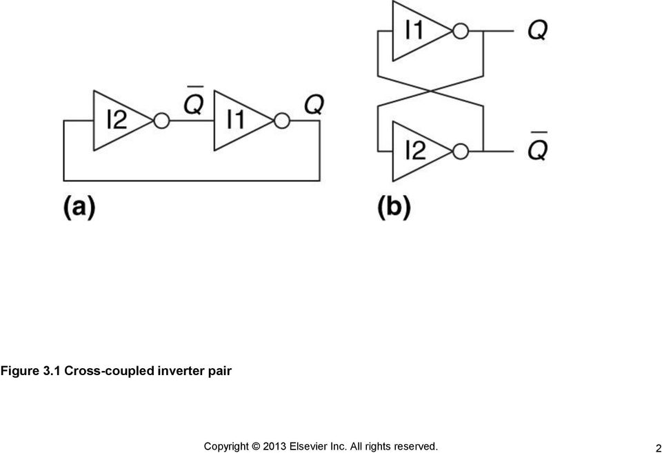
2 Figure 3.1 Cross-coupled inverter pair 2
3 Figure 3.2 Bistable operation of cross-coupled inverters 3

4 Figure 3.3 SR latch schematic 4

5 Figure 3.4 Bistable states of SR latch 5

6 Figure 3.5 SR latch truth table 6

7 Figure 3.6 SR latch symbol 7

8 Figure 3.7 D latch: (a) schematic, (b) truth table, (c) symbol 8

9 Figure 3.8 D flip-flop: (a) schematic, (b) symbol, (c) condensed symbol 9
")
10 Figure 3.9 A 4-bit register: (a) schematic and (b) symbol 10

11 Figure 3.10 Enabled flip-flop: (a, b) schematics, (c) symbol 11
 schematics,")
12 Figure 3.11 Synchronously resettable flip-flop: (a) schematic, (b, c) symbols 12
")
13 Figure 3.12 D latch schematic 13

14 Figure 3.13 D flip-flop schematic 14

15 Figure 3.14 Example waveforms 15

16 Figure 3.15 Solution waveforms 16

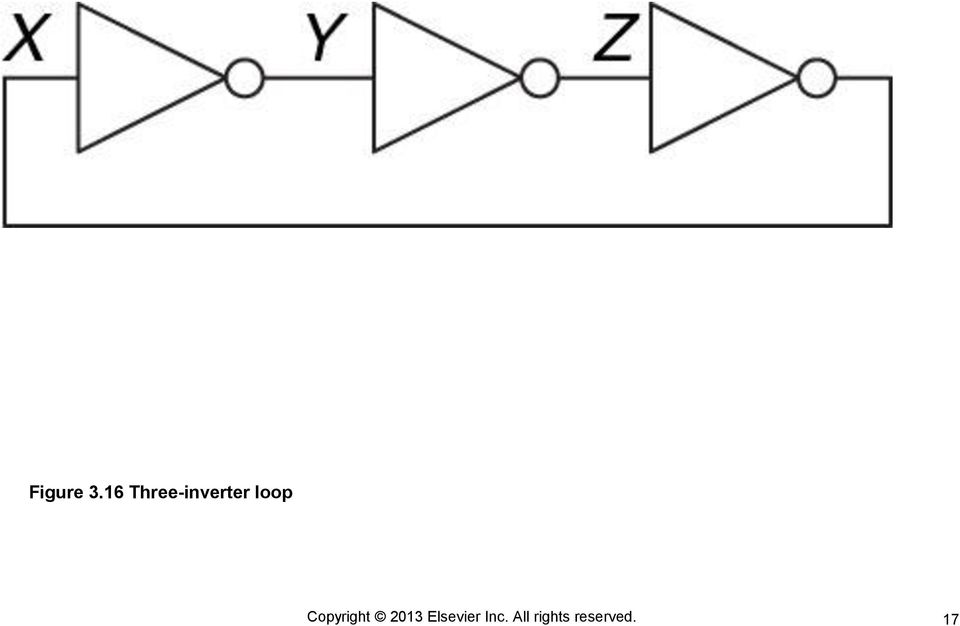
17 Figure 3.16 Three-inverter loop 17
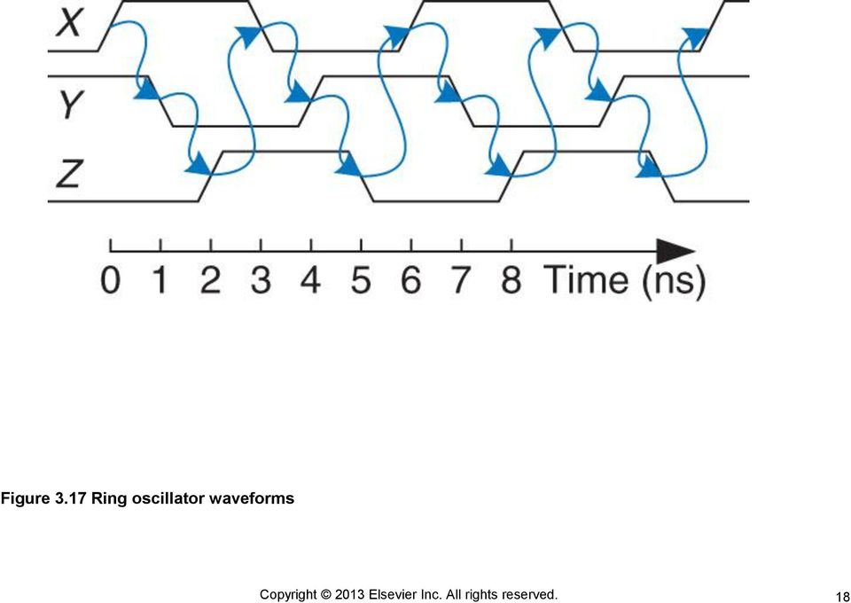
18 Figure 3.17 Ring oscillator waveforms 18
19 Figure 3.18 An improved (?) D latch 19
 D")
20 Figure 3.19 Latch waveforms illustrating race condition 20

21 Figure 3.20 Flip-flop current state and next state 21
22 Figure 3.21 Example circuits 22
23 Figure 3.22 Finite state machines: (a) Moore machine, (b) Mealy machine 23
24 Figure 3.23 Campus map 24
25 Figure 3.24 Black box view of finite state machine 25
26 Figure 3.25 State transition diagram 26
27 Figure 3.26 State machine circuit for traffic light controller 27
28 Figure 3.27 Timing diagram for traffic light controller 28
29 Figure 3.28 Divide-by-3 counter (a) waveform and (b) state transition diagram 29
30 Figure 3.29 Divide-by-3 circuits for (a) binary and (b) one-hot encodings 30
31 Figure 3.30 FSM state transition diagrams: (a) Moore machine, (b) Mealy machine 31
32 Figure 3.31 FSM schematics for (a) Moore and (b) Mealy machines 32
33 Figure 3.32 Timing diagrams for Moore and Mealy machines 33
34 Figure 3.33 (a) single and (b) factored designs for modified traffic light controller FSM 34
35 Figure 3.34 State transition diagrams: (a) unfactored, (b) factored 35
36 Figure 3.35 Circuit of found FSM for Example
37 Figure 3.36 State transition diagram of found FSM from Example
38 Figure 3.37 Timing specification for synchronous sequential circuit 38
39 Figure 3.38 Path between registers and timing diagram 39
40 Figure 3.39 Maximum delay for setup time constraint 40
41 Figure 3.40 Minimum delay for hold time constraint 41
42 Figure 3.41 Back-to-back flip-flops 42
43 Figure 3.42 Sample circuit for timing analysis 43
44 Figure 3.43 Timing diagram: (a) general case, (b) critical path, (c) short path 44
45 Figure 3.44 Corrected circuit to fix hold time problem 45
46 Figure 3.45 Timing diagram with buffers to fix hold time problem 46
47 Figure 3.46 Clock skew caused by wire delay 47
48 Figure 3.47 Timing diagram with clock skew 48
49 Figure 3.48 Setup time constraint with clock skew 49
50 Figure 3.49 Hold time constraint with clock skew 50
51 Figure 3.50 Input changing before, after, or during aperture 51
52 Figure 3.51 Stable and metastable states 52
53 Figure 3.52 Synchronizer symbol 53
54 Figure 3.53 Simple synchronizer 54
55 Figure 3.54 Input timing 55
56 Figure 3.55 Circuit model of bistable device 56
57 Figure 3.56 Resolution trajectories 57
58 Figure 3.57 Spatial and temporal parallelism in the cookie kitchen 58
59 Figure 3.58 Circuit with no pipelining 59
60 Figure 3.59 Circuit with two-stage pipeline 60
61 Figure 3.60 Circuit with three-stage pipeline 61
62 Figure 3.61 Input waveforms of SR latch for Exercise
63 Figure 3.62 Input waveforms of SR latch for Exercise
64 Figure 3.63 Input waveforms of D latch or flip-flop for Exercises 3.3 and
65 Figure 3.64 Input waveforms of D latch or flip-flop for Exercises 3.4 and
66 Figure 3.65 Mystery circuit 66
67 Figure 3.66 Mystery circuit 67
68 Figure 3.67 Muller C-element 68
69 Figure 3.68 Circuits 69
70 Figure 3.69 State transition diagram 70
71 Figure 3.70 State transition diagram 71
72 Figure 3.71 FSM input waveforms 72
73 Figure 3.72 FSM schematic 73
74 Figure 3.73 FSM schematic 74
75 Figure 3.74 Registered four-input XOR circuit 75
76 Figure bit adder schematic 76
77 Figure 3.76 New and improved synchronizer 77
78 Figure 3.77 Signal waveforms 78
79 Figure M 01 79
80 Figure M 02 80
81 Figure M 03 81
82 Figure M 04 82
83 Figure M 05 83
84 UNN Figure 1 84
EE 42/100 Lecture 24: Latches and Flip Flops. Rev B 4/21/2010 (2:04 PM) Prof. Ali M. Niknejad
 Prof. Ali M. Niknejad") A. M. Niknejad University of California, Berkeley EE 100 / 42 Lecture 24 p. 1/20 EE 42/100 Lecture 24: Latches and Flip Flops ELECTRONICS Rev B 4/21/2010 (2:04 PM) Prof. Ali M. Niknejad University of California,
A. M. Niknejad University of California, Berkeley EE 100 / 42 Lecture 24 p. 1/20 EE 42/100 Lecture 24: Latches and Flip Flops ELECTRONICS Rev B 4/21/2010 (2:04 PM) Prof. Ali M. Niknejad University of California,
Lecture 8: Synchronous Digital Systems
 Lecture 8: Synchronous Digital Systems The distinguishing feature of a synchronous digital system is that the circuit only changes in response to a system clock. For example, consider the edge triggered
Digital Electronics Detailed Outline
 Digital Electronics Detailed Outline Unit 1: Fundamentals of Analog and Digital Electronics (32 Total Days) Lesson 1.1: Foundations and the Board Game Counter (9 days) 1. Safety is an important concept
Sequential Circuit Design
 Sequential Circuit Design Lan-Da Van ( 倫 ), Ph. D. Department of Computer Science National Chiao Tung University Taiwan, R.O.C. Fall, 2009 [email protected] http://www.cs.nctu.edu.tw/~ldvan/ Outlines
Flip-Flops and Sequential Circuit Design. ECE 152A Winter 2012
 Flip-Flops and Sequential Circuit Design ECE 52 Winter 22 Reading ssignment Brown and Vranesic 7 Flip-Flops, Registers, Counters and a Simple Processor 7.5 T Flip-Flop 7.5. Configurable Flip-Flops 7.6
Flip-Flops and Sequential Circuit Design
 Flip-Flops and Sequential Circuit Design ECE 52 Winter 22 Reading ssignment Brown and Vranesic 7 Flip-Flops, Registers, Counters and a Simple Processor 7.5 T Flip-Flop 7.5. Configurable Flip-Flops 7.6
Topics of Chapter 5 Sequential Machines. Memory elements. Memory element terminology. Clock terminology
 Topics of Chapter 5 Sequential Machines Memory elements Memory elements. Basics of sequential machines. Clocking issues. Two-phase clocking. Testing of combinational (Chapter 4) and sequential (Chapter
Lecture 7: Clocking of VLSI Systems
 Lecture 7: Clocking of VLSI Systems MAH, AEN EE271 Lecture 7 1 Overview Reading Wolf 5.3 Two-Phase Clocking (good description) W&E 5.5.1, 5.5.2, 5.5.3, 5.5.4, 5.5.9, 5.5.10 - Clocking Note: The analysis
PROGETTO DI SISTEMI ELETTRONICI DIGITALI. Digital Systems Design. Digital Circuits Advanced Topics
 PROGETTO DI SISTEMI ELETTRONICI DIGITALI Digital Systems Design Digital Circuits Advanced Topics 1 Sequential circuit and metastability 2 Sequential circuit - FSM A Sequential circuit contains: Storage
Theory of Logic Circuits. Laboratory manual. Exercise 3
 Zakład Mikroinformatyki i Teorii Automatów yfrowych Theory of Logic ircuits Laboratory manual Exercise 3 Bistable devices 2008 Krzysztof yran, Piotr zekalski (edt.) 1. lassification of bistable devices
Introduction to CMOS VLSI Design (E158) Lecture 8: Clocking of VLSI Systems
 Lecture 8: Clocking of VLSI Systems") Harris Introduction to CMOS VLSI Design (E158) Lecture 8: Clocking of VLSI Systems David Harris Harvey Mudd College [email protected] Based on EE271 developed by Mark Horowitz, Stanford University MAH
Harris Introduction to CMOS VLSI Design (E158) Lecture 8: Clocking of VLSI Systems David Harris Harvey Mudd College [email protected] Based on EE271 developed by Mark Horowitz, Stanford University MAH
Flip-Flops, Registers, Counters, and a Simple Processor
 June 8, 22 5:56 vra235_ch7 Sheet number Page number 349 black chapter 7 Flip-Flops, Registers, Counters, and a Simple Processor 7. Ng f3, h7 h6 349 June 8, 22 5:56 vra235_ch7 Sheet number 2 Page number
Chapter 5. Sequential Logic
 Chapter 5 Sequential Logic Sequential Circuits (/2) Combinational circuits: a. contain no memory elements b. the outputs depends on the current inputs Sequential circuits: a feedback path outputs depends
ETEC 2301 Programmable Logic Devices. Chapter 10 Counters. Shawnee State University Department of Industrial and Engineering Technologies
 ETEC 2301 Programmable Logic Devices Chapter 10 Counters Shawnee State University Department of Industrial and Engineering Technologies Copyright 2007 by Janna B. Gallaher Asynchronous Counter Operation
CHAPTER 11 LATCHES AND FLIP-FLOPS
 CHAPTER 11 LATCHES AND FLIP-FLOPS This chapter in the book includes: Objectives Study Guide 11.1 Introduction 11.2 Set-Reset Latch 11.3 Gated D Latch 11.4 Edge-Triggered D Flip-Flop 11.5 S-R Flip-Flop
IE1204 Digital Design F12: Asynchronous Sequential Circuits (Part 1)
") IE1204 Digital Design F12: Asynchronous Sequential Circuits (Part 1) Elena Dubrova KTH / ICT / ES [email protected] BV pp. 584-640 This lecture IE1204 Digital Design, HT14 2 Asynchronous Sequential Machines
IE1204 Digital Design F12: Asynchronous Sequential Circuits (Part 1) Elena Dubrova KTH / ICT / ES [email protected] BV pp. 584-640 This lecture IE1204 Digital Design, HT14 2 Asynchronous Sequential Machines
Latch Timing Parameters. Flip-flop Timing Parameters. Typical Clock System. Clocking Overhead
 Clock - key to synchronous systems Topic 7 Clocking Strategies in VLSI Systems Peter Cheung Department of Electrical & Electronic Engineering Imperial College London Clocks help the design of FSM where
Finite State Machine. RTL Hardware Design by P. Chu. Chapter 10 1
 Finite State Machine Chapter 10 1 Outline 1. Overview 2. FSM representation 3. Timing and performance of an FSM 4. Moore machine versus Mealy machine 5. VHDL description of FSMs 6. State assignment 7.
Module 3: Floyd, Digital Fundamental
 Module 3: Lecturer : Yongsheng Gao Room : Tech - 3.25 Email : [email protected] Structure : 6 lectures 1 Tutorial Assessment: 1 Laboratory (5%) 1 Test (20%) Textbook : Floyd, Digital Fundamental
Sequential Logic Design Principles.Latches and Flip-Flops
 Sequential Logic Design Principles.Latches and Flip-Flops Doru Todinca Department of Computers Politehnica University of Timisoara Outline Introduction Bistable Elements Latches and Flip-Flops S-R Latch
Engr354: Digital Logic Circuits
 Engr354: igital Circuits Chapter 7 Sequential Elements r. Curtis Nelson Sequential Elements In this chapter you will learn about: circuits that can store information; Basic cells, latches, and flip-flops;
Sequential Logic: Clocks, Registers, etc.
 ENEE 245: igital Circuits & Systems Lab Lab 2 : Clocks, Registers, etc. ENEE 245: igital Circuits and Systems Laboratory Lab 2 Objectives The objectives of this laboratory are the following: To design
Combinational Logic Design Process
 Combinational Logic Design Process Create truth table from specification Generate K-maps & obtain logic equations Draw logic diagram (sharing common gates) Simulate circuit for design verification Debug
BINARY CODED DECIMAL: B.C.D.
 BINARY CODED DECIMAL: B.C.D. ANOTHER METHOD TO REPRESENT DECIMAL NUMBERS USEFUL BECAUSE MANY DIGITAL DEVICES PROCESS + DISPLAY NUMBERS IN TENS IN BCD EACH NUMBER IS DEFINED BY A BINARY CODE OF 4 BITS.
Latches, the D Flip-Flop & Counter Design. ECE 152A Winter 2012
 Latches, the D Flip-Flop & Counter Design ECE 52A Winter 22 Reading Assignment Brown and Vranesic 7 Flip-Flops, Registers, Counters and a Simple Processor 7. Basic Latch 7.2 Gated SR Latch 7.2. Gated SR
Lesson 12 Sequential Circuits: Flip-Flops
 Lesson 12 Sequential Circuits: Flip-Flops 1. Overview of a Synchronous Sequential Circuit We saw from last lesson that the level sensitive latches could cause instability in a sequential system. This instability
Digital Systems Based on Principles and Applications of Electrical Engineering/Rizzoni (McGraw Hill
 Digital Systems Based on Principles and Applications of Electrical Engineering/Rizzoni (McGraw Hill Objectives: Analyze the operation of sequential logic circuits. Understand the operation of digital counters.
So far we have investigated combinational logic for which the output of the logic devices/circuits depends only on the present state of the inputs.
 equential Logic o far we have investigated combinational logic for which the output of the logic devices/circuits depends only on the present state of the inputs. In sequential logic the output of the
Upon completion of unit 1.1, students will be able to
 Upon completion of unit 1.1, students will be able to 1. Demonstrate safety of the individual, class, and overall environment of the classroom/laboratory, and understand that electricity, even at the nominal
Having read this workbook you should be able to: recognise the arrangement of NAND gates used to form an S-R flip-flop.
 Objectives Having read this workbook you should be able to: recognise the arrangement of NAND gates used to form an S-R flip-flop. describe how such a flip-flop can be SET and RESET. describe the disadvantage
Sequential Logic. (Materials taken from: Principles of Computer Hardware by Alan Clements )
") Sequential Logic (Materials taken from: Principles of Computer Hardware by Alan Clements ) Sequential vs. Combinational Circuits Combinatorial circuits: their outputs are computed entirely from their present
Sequential Logic (Materials taken from: Principles of Computer Hardware by Alan Clements ) Sequential vs. Combinational Circuits Combinatorial circuits: their outputs are computed entirely from their present
Memory Elements. Combinational logic cannot remember
 Memory Elements Combinational logic cannot remember Output logic values are function of inputs only Feedback is needed to be able to remember a logic value Memory elements are needed in most digital logic
Digital Logic Design. Basics Combinational Circuits Sequential Circuits. Pu-Jen Cheng
 Digital Logic Design Basics Combinational Circuits Sequential Circuits Pu-Jen Cheng Adapted from the slides prepared by S. Dandamudi for the book, Fundamentals of Computer Organization and Design. Introduction
Clocking. Figure by MIT OCW. 6.884 - Spring 2005 2/18/05 L06 Clocks 1
 ing Figure by MIT OCW. 6.884 - Spring 2005 2/18/05 L06 s 1 Why s and Storage Elements? Inputs Combinational Logic Outputs Want to reuse combinational logic from cycle to cycle 6.884 - Spring 2005 2/18/05
Design Example: Counters. Design Example: Counters. 3-Bit Binary Counter. 3-Bit Binary Counter. Other useful counters:
 Design Eample: ers er: a sequential circuit that repeats a specified sequence of output upon clock pulses. A,B,C,, Z. G, O, T, E, R, P, S,!.,,,,,,,7. 7,,,,,,,.,,,,,,,,,,,. Binary counter: follows the binary
CS311 Lecture: Sequential Circuits
 CS311 Lecture: Sequential Circuits Last revised 8/15/2007 Objectives: 1. To introduce asynchronous and synchronous flip-flops (latches and pulsetriggered, plus asynchronous preset/clear) 2. To introduce
Counters are sequential circuits which "count" through a specific state sequence.
 Counters Counters are sequential circuits which "count" through a specific state sequence. They can count up, count down, or count through other fixed sequences. Two distinct types are in common usage:
SEQUENTIAL CIRCUITS. Block diagram. Flip Flop. S-R Flip Flop. Block Diagram. Circuit Diagram
 SEQUENTIAL CIRCUITS http://www.tutorialspoint.com/computer_logical_organization/sequential_circuits.htm Copyright tutorialspoint.com The combinational circuit does not use any memory. Hence the previous
Counters. Present State Next State A B A B 0 0 0 1 0 1 1 0 1 0 1 1 1 1 0 0
 ounter ounters ounters are a specific type of sequential circuit. Like registers, the state, or the flip-flop values themselves, serves as the output. The output value increases by one on each clock cycle.
Lecture 11: Sequential Circuit Design
 Lecture 11: Sequential Circuit esign Outline Sequencing Sequencing Element esign Max and Min-elay Clock Skew Time Borrowing Two-Phase Clocking 2 Sequencing Combinational logic output depends on current
Lecture 10: Sequential Circuits
 Introduction to CMOS VLSI esign Lecture 10: Sequential Circuits avid Harris Harvey Mudd College Spring 2004 Outline q Sequencing q Sequencing Element esign q Max and Min-elay q Clock Skew q Time Borrowing
Digital Electronics Part I Combinational and Sequential Logic. Dr. I. J. Wassell
 Digital Electronics Part I Combinational and Sequential Logic Dr. I. J. Wassell Introduction Aims To familiarise students with Combinational logic circuits Sequential logic circuits How digital logic gates
Sequential Circuits. Combinational Circuits Outputs depend on the current inputs
 Principles of VLSI esign Sequential Circuits Sequential Circuits Combinational Circuits Outputs depend on the current inputs Sequential Circuits Outputs depend on current and previous inputs Requires separating
Lecture 10 Sequential Circuit Design Zhuo Feng. Z. Feng MTU EE4800 CMOS Digital IC Design & Analysis 2010
 EE4800 CMOS igital IC esign & Analysis Lecture 10 Sequential Circuit esign Zhuo Feng 10.1 Z. Feng MTU EE4800 CMOS igital IC esign & Analysis 2010 Sequencing Outline Sequencing Element esign Max and Min-elay
Layout of Multiple Cells
 Layout of Multiple Cells Beyond the primitive tier primitives add instances of primitives add additional transistors if necessary add substrate/well contacts (plugs) add additional polygons where needed
Chapter 4 Register Transfer and Microoperations. Section 4.1 Register Transfer Language
 Chapter 4 Register Transfer and Microoperations Section 4.1 Register Transfer Language Digital systems are composed of modules that are constructed from digital components, such as registers, decoders,
Chapter 8. Sequential Circuits for Registers and Counters
 Chapter 8 Sequential Circuits for Registers and Counters Lesson 3 COUNTERS Ch16L3- "Digital Principles and Design", Raj Kamal, Pearson Education, 2006 2 Outline Counters T-FF Basic Counting element State
Set-Reset (SR) Latch
 Latch") et-eset () Latch Asynchronous Level sensitive cross-coupled Nor gates active high inputs (only one can be active) + + Function 0 0 0 1 0 1 eset 1 0 1 0 et 1 1 0-? 0-? Indeterminate cross-coupled Nand gates
et-eset () Latch Asynchronous Level sensitive cross-coupled Nor gates active high inputs (only one can be active) + + Function 0 0 0 1 0 1 eset 1 0 1 0 et 1 1 0-? 0-? Indeterminate cross-coupled Nand gates
Gates, Circuits, and Boolean Algebra
 Gates, Circuits, and Boolean Algebra Computers and Electricity A gate is a device that performs a basic operation on electrical signals Gates are combined into circuits to perform more complicated tasks
Experiment # 9. Clock generator circuits & Counters. Eng. Waleed Y. Mousa
 Experiment # 9 Clock generator circuits & Counters Eng. Waleed Y. Mousa 1. Objectives: 1. Understanding the principles and construction of Clock generator. 2. To be familiar with clock pulse generation
ASYNCHRONOUS COUNTERS
 LB no.. SYNCHONOUS COUNTES. Introduction Counters are sequential logic circuits that counts the pulses applied at their clock input. They usually have 4 bits, delivering at the outputs the corresponding
WEEK 8.1 Registers and Counters. ECE124 Digital Circuits and Systems Page 1
 WEEK 8.1 egisters and Counters ECE124 igital Circuits and Systems Page 1 Additional schematic FF symbols Active low set and reset signals. S Active high set and reset signals. S ECE124 igital Circuits
Asynchronous Counters. Asynchronous Counters
 Counters and State Machine Design November 25 Asynchronous Counters ENGI 25 ELEC 24 Asynchronous Counters The term Asynchronous refers to events that do not occur at the same time With respect to counter
More Verilog. 8-bit Register with Synchronous Reset. Shift Register Example. N-bit Register with Asynchronous Reset.
 More Verilog 8-bit Register with Synchronous Reset module reg8 (reset, CLK, D, Q); input reset; input [7:0] D; output [7:0] Q; reg [7:0] Q; if (reset) Q = 0; else Q = D; module // reg8 Verilog - 1 Verilog
ECE232: Hardware Organization and Design. Part 3: Verilog Tutorial. http://www.ecs.umass.edu/ece/ece232/ Basic Verilog
 ECE232: Hardware Organization and Design Part 3: Verilog Tutorial http://www.ecs.umass.edu/ece/ece232/ Basic Verilog module ();
LAB #4 Sequential Logic, Latches, Flip-Flops, Shift Registers, and Counters
 LAB #4 Sequential Logic, Latches, Flip-Flops, Shift Registers, and Counters LAB OBJECTIVES 1. Introduction to latches and the D type flip-flop 2. Use of actual flip-flops to help you understand sequential
L4: Sequential Building Blocks (Flip-flops, Latches and Registers)
") L4: Sequential Building Blocks (Flip-flops, Latches and Registers) Acknowledgements: Materials in this lecture are courtesy of the following sources and are used with permission. Prof. Randy Katz (Unified
L4: Sequential Building Blocks (Flip-flops, Latches and Registers) Acknowledgements: Materials in this lecture are courtesy of the following sources and are used with permission. Prof. Randy Katz (Unified
Aims and Objectives. E 3.05 Digital System Design. Course Syllabus. Course Syllabus (1) Programmable Logic
 Programmable Logic") Aims and Objectives E 3.05 Digital System Design Peter Cheung Department of Electrical & Electronic Engineering Imperial College London URL: www.ee.ic.ac.uk/pcheung/ E-mail: [email protected] How to go
Aims and Objectives E 3.05 Digital System Design Peter Cheung Department of Electrical & Electronic Engineering Imperial College London URL: www.ee.ic.ac.uk/pcheung/ E-mail: [email protected] How to go
CHAPTER 3 Boolean Algebra and Digital Logic
 CHAPTER 3 Boolean Algebra and Digital Logic 3.1 Introduction 121 3.2 Boolean Algebra 122 3.2.1 Boolean Expressions 123 3.2.2 Boolean Identities 124 3.2.3 Simplification of Boolean Expressions 126 3.2.4
CDA 3200 Digital Systems. Instructor: Dr. Janusz Zalewski Developed by: Dr. Dahai Guo Spring 2012
 CDA 3200 Digital Systems Instructor: Dr. Janusz Zalewski Developed by: Dr. Dahai Guo Spring 2012 Outline SR Latch D Latch Edge-Triggered D Flip-Flop (FF) S-R Flip-Flop (FF) J-K Flip-Flop (FF) T Flip-Flop
7. Latches and Flip-Flops
 Chapter 7 Latches and Flip-Flops Page 1 of 18 7. Latches and Flip-Flops Latches and flip-flops are the basic elements for storing information. One latch or flip-flop can store one bit of information. The
Chapter 9 Latches, Flip-Flops, and Timers
 ETEC 23 Programmable Logic Devices Chapter 9 Latches, Flip-Flops, and Timers Shawnee State University Department of Industrial and Engineering Technologies Copyright 27 by Janna B. Gallaher Latches A temporary
Modeling Sequential Elements with Verilog. Prof. Chien-Nan Liu TEL: 03-4227151 ext:34534 Email: [email protected]. Sequential Circuit
 Modeling Sequential Elements with Verilog Prof. Chien-Nan Liu TEL: 03-4227151 ext:34534 Email: [email protected] 4-1 Sequential Circuit Outputs are functions of inputs and present states of storage elements
EE552. Advanced Logic Design and Switching Theory. Metastability. Ashirwad Bahukhandi. (Ashirwad Bahukhandi) [email protected]
 bahukhan@usc.edu") EE552 Advanced Logic Design and Switching Theory Metastability by Ashirwad Bahukhandi (Ashirwad Bahukhandi) [email protected] This is an overview of what metastability is, ways of interpreting it, the issues
EE552 Advanced Logic Design and Switching Theory Metastability by Ashirwad Bahukhandi (Ashirwad Bahukhandi) [email protected] This is an overview of what metastability is, ways of interpreting it, the issues
Counters and Decoders
 Physics 3330 Experiment #10 Fall 1999 Purpose Counters and Decoders In this experiment, you will design and construct a 4-bit ripple-through decade counter with a decimal read-out display. Such a counter
Finite State Machine Design A Vending Machine
 LAB 6 Finite State Machine Design A Vending Machine You will learn how turn an informal sequential circuit description into a formal finite-state machine model, how to express it using ABEL, how to simulate
Sequential 4-bit Adder Design Report
 UNIVERSITY OF WATERLOO Faculty of Engineering E&CE 438: Digital Integrated Circuits Sequential 4-bit Adder Design Report Prepared by: Ian Hung (ixxxxxx), 99XXXXXX Annette Lo (axxxxxx), 99XXXXXX Pamela
CS 61C: Great Ideas in Computer Architecture Finite State Machines. Machine Interpreta4on
 CS 61C: Great Ideas in Computer Architecture Finite State Machines Instructors: Krste Asanovic & Vladimir Stojanovic hbp://inst.eecs.berkeley.edu/~cs61c/sp15 1 Levels of RepresentaKon/ InterpretaKon High
1. True or False? A voltage level in the range 0 to 2 volts is interpreted as a binary 1.
 File: chap04, Chapter 04 1. True or False? A voltage level in the range 0 to 2 volts is interpreted as a binary 1. 2. True or False? A gate is a device that accepts a single input signal and produces one
List of Experiment. 8. To study and verify the BCD to Seven Segments DECODER.(IC-7447).
.") G. H. RAISONI COLLEGE OF ENGINEERING, NAGPUR Department of Electronics & Communication Engineering Branch:-4 th Semester[Electronics] Subject: - Digital Circuits List of Experiment Sr. Name Of Experiment
G. H. RAISONI COLLEGE OF ENGINEERING, NAGPUR Department of Electronics & Communication Engineering Branch:-4 th Semester[Electronics] Subject: - Digital Circuits List of Experiment Sr. Name Of Experiment
Digital Fundamentals
 igital Fundamentals with PL Programming Floyd Chapter 9 Floyd, igital Fundamentals, 10 th ed, Upper Saddle River, NJ 07458. All Rights Reserved Summary Latches (biestables) A latch is a temporary storage
ENEE 244 (01**). Spring 2006. Homework 5. Due back in class on Friday, April 28.
. Spring 2006. Homework 5. Due back in class on Friday, April 28.") ENEE 244 (01**). Spring 2006 Homework 5 Due back in class on Friday, April 28. 1. Fill up the function table (truth table) for the following latch. How is this latch related to those described in the lectures
ENEE 244 (01**). Spring 2006 Homework 5 Due back in class on Friday, April 28. 1. Fill up the function table (truth table) for the following latch. How is this latch related to those described in the lectures
A New Paradigm for Synchronous State Machine Design in Verilog
 A New Paradigm for Synchronous State Machine Design in Verilog Randy Nuss Copyright 1999 Idea Consulting Introduction Synchronous State Machines are one of the most common building blocks in modern digital
CONTENTS PREFACE 1 INTRODUCTION 1 2 NUMBER SYSTEMS AND CODES 25. vii
 2006 Pearson Education, Inc., Upper Saddle River, NJ. All rights reserved. This material is CONTENTS PREFACE xv 1 INTRODUCTION 1 1.1 About Digital Design 1 1.2 Analog versus Digital 3 1.3 Digital Devices
路 論 Chapter 15 System-Level Physical Design
 Introduction to VLSI Circuits and Systems 路 論 Chapter 15 System-Level Physical Design Dept. of Electronic Engineering National Chin-Yi University of Technology Fall 2007 Outline Clocked Flip-flops CMOS
COMBINATIONAL and SEQUENTIAL LOGIC CIRCUITS Hardware implementation and software design
 PH-315 COMINATIONAL and SEUENTIAL LOGIC CIRCUITS Hardware implementation and software design A La Rosa I PURPOSE: To familiarize with combinational and sequential logic circuits Combinational circuits
Lecture-3 MEMORY: Development of Memory:
 Lecture-3 MEMORY: It is a storage device. It stores program data and the results. There are two kind of memories; semiconductor memories & magnetic memories. Semiconductor memories are faster, smaller,
Timing Methodologies (cont d) Registers. Typical timing specifications. Synchronous System Model. Short Paths. System Clock Frequency
 Registers. Typical timing specifications. Synchronous System Model. Short Paths. System Clock Frequency") Registers Timing Methodologies (cont d) Sample data using clock Hold data between clock cycles Computation (and delay) occurs between registers efinition of terms setup time: minimum time before the clocking
Registers Timing Methodologies (cont d) Sample data using clock Hold data between clock cycles Computation (and delay) occurs between registers efinition of terms setup time: minimum time before the clocking
Academic year: 2015/2016 Code: IES-1-307-s ECTS credits: 6. Field of study: Electronics and Telecommunications Specialty: -
 Module name: Digital Electronics and Programmable Devices Academic year: 2015/2016 Code: IES-1-307-s ECTS credits: 6 Faculty of: Computer Science, Electronics and Telecommunications Field of study: Electronics
Registers & Counters
 Objectives This section deals with some simple and useful sequential circuits. Its objectives are to: Introduce registers as multi-bit storage devices. Introduce counters by adding logic to registers implementing
The components. E3: Digital electronics. Goals:
 E3: Digital electronics Goals: Basic understanding of logic circuits. Become familiar with the most common digital components and their use. Equipment: 1 st. LED bridge 1 st. 7-segment display. 2 st. IC
2 : BISTABLES. In this Chapter, you will find out about bistables which are the fundamental building blocks of electronic counting circuits.
 2 : BITABLE In this Chapter, you will find out about bistables which are the fundamental building blos of electronic counting circuits. et-reset bistable A bistable circuit, also called a latch, or flip-flop,
CHAPTER 16 MEMORY CIRCUITS
 CHPTER 6 MEMORY CIRCUITS Chapter Outline 6. atches and Flip-Flops 6. Semiconductor Memories: Types and rchitectures 6.3 Random-ccess Memory RM Cells 6.4 Sense-mplifier and ddress Decoders 6.5 Read-Only
Admin. ECE 550: Fundamentals of Computer Systems and Engineering. Last time. VHDL: Behavioral vs Structural. Memory Elements
 Admin C 55: Fundamentals of Computer ystems and ngineering torage and Clocking eading Finish up Chapter ecitation How is it going? VHL questions/issues? Homework Homework ubmissions vis akai C 55 (Hilton):
CpE358/CS381. Switching Theory and Logical Design. Class 10
 CpE358/CS38 Switching Theory and Logical Design Class CpE358/CS38 Summer- 24 Copyright 24-373 Today Fundamental concepts of digital systems (Mano Chapter ) Binary codes, number systems, and arithmetic
DIGITAL COUNTERS. Q B Q A = 00 initially. Q B Q A = 01 after the first clock pulse.
 DIGITAL COUNTERS http://www.tutorialspoint.com/computer_logical_organization/digital_counters.htm Copyright tutorialspoint.com Counter is a sequential circuit. A digital circuit which is used for a counting
PROGETTO DI SISTEMI ELETTRONICI DIGITALI. Digital Systems Design. Digital Circuits Advanced Topics
 PROGETTO DI SISTEMI ELETTRONICI DIGITALI Digital Systems Design Digital Circuits Advanced Topics 1 Sequential circuit and metastability 2 Sequential circuit A Sequential circuit contains: Storage elements:
Topics. Flip-flop-based sequential machines. Signals in flip-flop system. Flip-flop rules. Latch-based machines. Two-sided latch constraint
 Topics Flip-flop-based sequential machines! Clocking disciplines. Flip-flop rules! Primary inputs change after clock (φ) edge.! Primary inputs must stabilize before next clock edge.! Rules allow changes
DIGITAL TECHNICS II. Dr. Bálint Pődör. Óbuda University, Microelectronics and Technology Institute
 DIGITAL TECHNICS II Dr. Bálint Pődör Óbuda University, Microelectronics and Technology Institute 2. LECTURE: ELEMENTARY SEUENTIAL CIRCUITS: FLIP-FLOPS 1st year BSc course 2nd (Spring) term 2012/2013 1
DEPARTMENT OF INFORMATION TECHNLOGY
 DRONACHARYA GROUP OF INSTITUTIONS, GREATER NOIDA Affiliated to Mahamaya Technical University, Noida Approved by AICTE DEPARTMENT OF INFORMATION TECHNLOGY Lab Manual for Computer Organization Lab ECS-453
CSE140: Components and Design Techniques for Digital Systems
 CE4: Components and esign Techniques for igital ystems Tajana imunic osing ources: Where we are now What we ve covered so far (Chap -5, App. A& B) Number representations Boolean algebra OP and PO Logic
Asynchronous counters, except for the first block, work independently from a system clock.
 Counters Some digital circuits are designed for the purpose of counting and this is when counters become useful. Counters are made with flip-flops, they can be asynchronous or synchronous and they can
Fundamentals of Digital Electronics
 Fundamentals of Digital Electronics by Professor Barry Paton Dalhousie University March 998 Edition Part Number 32948A- Fundamentals of Digital Electronics Copyright Copyright 998 by National Instruments
The 104 Duke_ACC Machine
 The 104 Duke_ACC Machine The goal of the next two lessons is to design and simulate a simple accumulator-based processor. The specifications for this processor and some of the QuartusII design components
CHAPTER IX REGISTER BLOCKS COUNTERS, SHIFT, AND ROTATE REGISTERS
 CHAPTER IX-1 CHAPTER IX CHAPTER IX COUNTERS, SHIFT, AN ROTATE REGISTERS REA PAGES 249-275 FROM MANO AN KIME CHAPTER IX-2 INTROUCTION -INTROUCTION Like combinational building blocks, we can also develop
PLL frequency synthesizer
 ANALOG & TELECOMMUNICATION ELECTRONICS LABORATORY EXERCISE 4 Lab 4: PLL frequency synthesizer 1.1 Goal The goals of this lab exercise are: - Verify the behavior of a and of a complete PLL - Find capture
Digital Fundamentals. Lab 8 Asynchronous Counter Applications
 Richland College Engineering Technology Rev. 0 B. Donham Rev. 1 (7/2003). Horne Rev. 2 (1/2008). Bradbury Digital Fundamentals CETT 1425 Lab 8 Asynchronous Counter Applications Name: Date: Objectives:
Modeling Registers and Counters
 Lab Workbook Introduction When several flip-flops are grouped together, with a common clock, to hold related information the resulting circuit is called a register. Just like flip-flops, registers may
Design: a mod-8 Counter
 Design: a mod-8 Counter A mod-8 counter stores a integer value, and increments that value (say) on each clock tick, and wraps around to 0 if the previous stored value was 7. So, the stored value follows