PROGETTO DI SISTEMI ELETTRONICI DIGITALI. Digital Systems Design. Digital Circuits Advanced Topics
|
|
|
- Nigel Hodge
- 8 years ago
- Views:
Transcription
1 PROGETTO DI SISTEMI ELETTRONICI DIGITALI Digital Systems Design Digital Circuits Advanced Topics 1

2 Sequential circuit and metastability 2
3 Sequential circuit - FSM A Sequential circuit contains: Storage elements: Latches or Flip-Flops Inputs Outputs Combinational Logic: Implements a multiple-output switching function Inputs are signals from the outside. Outputs are signals to the outside. Other inputs, State or Present State, are signals from storage elements. The remaining outputs, Next State are inputs to storage elements State Storage Elements Combina -tional Logic Next State 3

4 Bistable element the basic memory block Has two stable conditions (states) Can be used to store binary symbols If Q = high, the feedback to inverter 2 will cause its output to be low, which also forces the output of inverter 1 to be high. So this is a stable state. If Q = low, the feedback to inverter 2 will cause its output to be high, which also forces the output of inverter 1 to be low. So this is the second stable state. 4

5 Synchronous and Asynchronous Sequential Circuits Asynchronous sequential circuits: Outputs and state change as soon as an input changes. Synchronous sequential circuits: Outputs and state change depending on a special input (clock). The term asynchronous is because the two flip-flops are not clocked by the same signal. The following circuit is also called asynchronous, 2-bit, binary up counter: 5

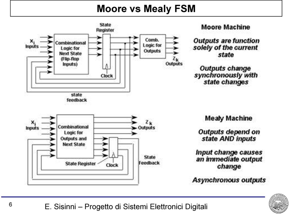
6 Moore vs Mealy FSM 6
7 Latch vs. Flip-flop Latch D D Q Q En En E D Y Level sensitive Flip-flop D D Q Q Clk Clk C D Q Edge-sensitive 7

8 Synchronous design Combinational Logic (Larger circuits difficult to predict) Synchronous Logic driven by a CLOCK Registers, Flip Flops (Memory) Intermediate Inputs New Output every clock edge CLOCK Register EDGES 8

9 Synchronous design rules All flip-flops are clocked only by the same free-running master clock. No latches No asynchronous feedback No clock signals are derived from logic gating (unless gating produced by tool, i.e., correct by construction) Asynchronous flip-flop inputs (Preset or Clear) are used only for initialization. Delays from one flip-flop to another flip-flop are designed to be less than the clock period. Asynchronous inputs pass through flip-flops (one or more) before being used elsewhere. Enable (control) signals are nominally one clock period in length. Note: Synchronous design is not always the best method, but it is to be assumed unless other methods are absolutely necessary. 9
 before being used elsewhere. Enable (control) signals are nominally one clock period in length.")
10 Timing Waveforms (asynchronous) A B C Y 0 ns 10 ns20 ns 30 ns 40 ns 50 ns 60 ns A B C Y 10

11 Timing Waveforms (synchronous) A B A_r B_r C D Clk Q 0 ns 10 ns 20 ns 30 ns 40 ns 50 ns 60 ns A B Clk D C D C Q Q A_r B_r C D D Q C Q_r 11

12 Metastability In an asynchronous system, the relationship between data and clock is not fixed; therefore, violations of setup and hold times can occur. When this happens, the output may go to an intermediate level between its two valid states and remain there for an indefinite amount of time before resolving itself or it may simply be delayed before making a normal transition. Two stable points, one metastable point: 12

13 Single-Stage Synchronizer - Metastability Minimum data set-up (tsu) and hold (thd) times must be met for the register to output synchronized data. The data input to the D flip-flop is asynchronous to the clock. The arrival time of the input data relative to the clock is not known and a danger zone (decision or metastability window) is created. After a clock-to-output delay (tco), the input data appears at the Q output. If the input data enters the danger zone, the Q output is likely to be in a metastable state until the internal silicon settles to either a logic high or low. The extra time required to resolve the logic state is called resolution time (tr). 13
, the input data appears at the Q output.")
14 Timing Waveforms (Metastability) Clk D_early Q_early D_late Q_late D_bad Q_bad 0 ns 10 ns 20 ns 30 ns 40 ns 50 ns 60 ns D D Q Changes before setup time Changes after hold time Changes after setup time or before hold time Indeterminate Q Clk C 14

15 Resolving the metastability The Resolving Time Constant, =1/, comes from the expression that describes the probability of a metastable event lasting longer than some time, t. If a FF is in the metastable state at time t its probability of resolve it over an additional time period Δt is the same regardless of the present age t The time to solve the metastability must follow an exponential probability distribution. Thus the probability that the system is still in the metastable state at time t is: 15

16 Calculating the MTBF Mean (Average) Time Between Failures or MTBF of a system, is the reciprocal of the failure rate in the special case when the failure rate is constant, i.e. distributed exponentially Failure rate = Metastability Rate * Probability of Metastability The probability of a metastable event lasting longer than some time is R(t): exp(-t/ ) Assume the data arrives uniformly over clock cycle T. The probability that data will arrive in W in a clock period T is: P = W/T = W fc, where: W = Metastability window and fc = Clock frequency If the data rate is fd, then the rate of metastability becomes W fc fd Failure rate = W fc fd exp(-tr/ ) MTBF = exp(tr/ ) /(W fc fd) T 16

17 Avoiding metastability The most common way to avoid metastability is to add one or more synchronizing FFs at the signals that move from one clock domain to the other. This approach allows for an entire clock period (except for the setup time of the following flip-flop) for metastable events to resolve itself. This does however increases the latency in observation of input. If clock frequency is fc=1/t, the resolution time for FF2 is bounded by T-T SU2, i.e. the MTBF is: MTBF FF2 = exp(t-t SU2 / ) /(W fc fd) 17

18 Avoiding metastability MTBF for different resolution time 18

19 Estimating device parameters A stable synchronous source is used for the measurement. The set-up and hold times of the input data relative to the clock can be adjusted while observing the Q output for the metastable event. The Metastability Window, W, can be determined by accurately measuring the Clock-To-Output Propagation Delay Time (tco) When the Set-up time or Hold time is violated, the Clock-To-Output Delay is increased. When the tco is measured longer than the tco_max (specified in the device data sheet), the device is considered to be in the metastable state 19

20 FPGA - Timing Analysis 20

21 Timing analysis Enables you to determine the delays between any pair of cells in your design Checks if your circuit will work under specified conditions Your circuit may be functionally correct and still not work On-chip What is the maximum clock frequency your design can run at? Are there any problems in the implementation due to timing? Off-chip Can your design on the FPGA can communicate with external devices reliably? 21
22 Timing analysis Static: Determine the longest and shortest path between register to register or register to I/O boundary. No function verification No test pattern. Each block must have a time model. Dynamic: inputs are considered Combinational Logic Combinational Logic clk 22
23 Timing analysis Clock setup time (tsu) Data that feeds a register via its data or enable input(s) must arrive at the input pin before the register s clock signal is asserted at the clock pin. Clock setup time is the minimum length of time that this data must arrive before the active clock edge Micro tsu is the intrinsic setup time of the register (i.e., it is an inherent characteristic of the register and is unaffected by the signals feeding the register). 23
24 Timing analysis Clock hold time (th) Data that feeds a register via its data or enable input(s) must be held at an input pin after the register s clock signal is asserted at the clock pin. Clock hold time is the minimum length of time that this data must be stable after the active clock edge Micro th is the intrinsic hold time of the register 24
25 Timing analysis Clock-to-output time (tco) Clock-to-output delay is the time required for a clock signal to travel from an input pin through a register to an output pin. This time always represents an external pin-to-pin delay. Micro tco is the intrinsic clock-tooutput delay of the register 25
26 Timing analysis Clock Skew Clock skew is the difference in arrival time of a clock signal at two different registers. This timing difference occurs when two clock signal paths have different lengths. Maximum Clock Frequency (fmax) Maximum clock frequency is the fastest speed the design clock can run without violating internal setup and hold time requirements. Slack Slack is the margin by which a timing requirement (e.g., fmax) was met or not met. A positive slack indicates that the circuit met the timing requirements; negative slack indicates that the design contains timing violations. 26
27 Timing analysis Calculating Internal fmax To determine internal fmax, you must first calculate the circuit s clock period. The clock period depends on the data path delay, the clock skew between registers, the source register s clock-to-output time, and the destination register s setup time. The Register-to-register delay (trd) in the clock period equation represents the data path delay between two registers. System fmax System fmax includes external delays, assuming that all input pins are registered just before entering the device, and all output pins are registered just after leaving the device. 27
28 Timing analysis Internal fmax; Register-to-Register Transfer minimum clock period (maximum clock frequency) w clk a b z w clk a b z Tmin=1/fmax= Sµt co B Dµt su +(C-E):t clk_skew 28
29 Timing analysis System fmax; clock period = 1/fmax_internal 29
30 Pipelining 30
31 Pipelining Clock frequency is defined as the rate at which data flows into the system and appears at the output. Pipelining decreases the combinational delay by inserting registers in a long combinational path, thus increasing the clock frequency and hence a higher performance. For a perfect clock without any jitter, the clock signal reaches all banks of registers simultaneously. If FFs are ideal (no tco, tsu and th): the maximum frequency FMAX is the reciprocal of the maximum delay path through the combinational logic. 31
32 FF and clock non idealities FF have delays: In real time circuit s clock input to register B would come after a small delay than at register A due to wire propagation delay: TSKW. Negative clock skew is due to early clocking i.e. clocking of registers before the relevant data is successfully latched. The variation between arrival times of the consecutive clock edges at the same point on the chip is defined as clock jitter TJIT. 32
33 Real world circuit Path in bold refers to the path with maximum delay between any two flip-flops in the circuit: 33
34 Real world circuit The total delay between the two flip-flops along the path b,f,j,l,m,n,o is: Assuming equal delays across all the flip-flops in design (which might not be the actual case) we have the generalized formula for the maximum period as: The combinational delay in the above equation can be reduced by adding more FFs, thus increasing the max frequency on which a circuit can operate. 34
35 Pipelining again! Pipelining splits the critical path (path with maximum combinational delay) with memory elements between the clock cycles increases the calculations per second since the clock period per stage is reduced but increases the overhead by adding memory elements 35
36 Performance Increase Consider a big array of combinational logic between registers. The latency of the circuit is also the clock period: Consider the same circuit to be pipelined into n stages: Pipeline stage with worst delay limits the clock period: The latency is n times the clock period: Ideally, each pipeline stage has equal delay: 36
37 Performance Increase So the minimum possible clock period for any pipeline stage is: Thus the final latency with this ideal clock period is: We can now calculate the speed increase of a circuit after pipelining: If we specify the register and clock overhead as a fraction k of the total clock period of an unpipelined circuit, then we have: 37
38 Clock gating and reset strategies 38
39 Clock gating In the traditional synchronous design style, the system clock is connected to the clock pin on every flip-flop in the design. This results in three major components of power consumption: 1. Power consumed by combinatorial logic whose values are changing on each clock edge (due to flops driving those combo cells). 2. Power consumed by flip-flops (this has non-zero value even if the inputs to the flip-flops, and therefore, the internal state of the flip-flops, is not changing). 3. Power consumed by the clock tree buffers in the design. Gating the clock path substantially reduces the power consumed by a Flip Flop. Gate clocking imposes that all enable signals be held constant from the active (rising) edge of the clock until the inactive (falling) edge of the clock to avoid truncating the generated clock pulse prematurely or generating multiple clock pulses (or glitches in clock): discard! 39
40 Clock gating The latch-based clock gating style adds a level-sensitive latch to the design to hold the enable signal from the active edge of the clock until the inactive edge of the clock. The latch captures the state of the enable signal and holds it until the complete clock pulse has been generated. The enable signal need only be stable around the rising edge of the clock. Only one input of the gate that turns the clock on and off changes at a time, ensuring that the circuit is free from any glitches or spikes on the output. 40
41 Synchronous reset Synchronous resets are based on the premise that the reset signal will only affect or reset the state of the flip-flop on the active edge of a clock. Advantages of Using Synchronous Resets Synchronous resets generally insure that the circuit is 100% synchronous. Synchronous reset logic will synthesize to smaller flip-flops, particularly if the reset is gated with the logic generating the Flop input. Synchronous resets ensure that reset can only occur at an active clock edge. The clock works as a filter for small reset glitches. Disadvantages Synchronous resets may need a pulse stretcher to guarantee a reset pulse width wide enough to ensure reset is present during an active edge of the clock. A synchronous reset will require a clock in order to reset the circuit. This may be a problem in some case where a gated clock is used to save power. 41
42 Gated Clocks vs Synchronous reset Q(7 downto 0) Eight bit binary counter with gated clock (not recommended) " " + D Q CountEn Clk C Q(7 downto 0) Eight bit binary counter with free-running clock (recommended) " " + CountEn 0 1 Clk D Q C 42
43 Asynchronous Reset Asynchronous reset flip-flops incorporate a reset pin into the flip-flop design. The most obvious advantage favoring asynchronous resets is that the circuit can be reset with or without a clock present. The biggest problem with asynchronous resets is that they are asynchronous, both at the assertion and at the de-assertion. The assertion is a non issue, the deassertion is the issue. If the asynchronous reset is released at or near the active clock edge of a flip-flop, the output of the flip-flop could go metastable. Another problem that an asynchronous reset can have, depending on its source, is spurious resets due to noise or glitches on the board or system reset. 43
44 Reset synchronizer The reset synchronizer logic is designed to take advantage of the best of both asynchronous and synchronous reset styles. An external reset signal asynchronously resets a pair of flip-flops, which in turn drive the master reset signal asynchronously through the reset buffer tree to the rest of the flip-flops in the design. The entire design will be asynchronously reset. 44
45 Reset Glitch Filtering 45
46 Multiple clock domains 46
47 Multiple Clock domains Designs with multiple clocks can have: clocks with different frequencies and/or clocks with same frequency but different phases between them. Metastability issues may arise; system desing must be partitioned so that each module should work on one clock only. A synchronizer module has to be made for all signals that cross from one clock domain to another 47
48 Synchronous Clock domain crossing Clocks originating from the same clock-root and having a known phase and frequency relationship between them are known as synchronous clocks. A clock crossing between such clocks is known as a synchronous clock domain crossing. Depending on frequency and phase relationship, synchronizers may be needed or not! Synchronous Clock domain crossing can be divided into several categories: Clocks with the same frequency and zero phase difference: no domain cross! 48
49 Synchronous Clock domain crossing Synchronous Clock domain crossing can be divided into several categories : Clocks with the same frequency and constant phase difference: tighter constraint on the combinational logic delay due to smaller setup/hold margins. Integer multiple clocks: the minimum possible phase difference between the active edges of the two clocks would always be equal to the time period of the fast clock, i.e. one complete cycle of the faster clock would always be available for sampling 49
50 Synchronous Clock domain crossing Synchronous Clock domain crossing can be divided into several categories. Rational multiple clocks: the minimum phase difference between the two clocks can be small enough to cause metastability: synchronization needs to be done! 50
51 Transfer of control signals Two or more flip-flops are cascaded to form a synchronizing circuit As previously seen, if the first flop of a synchronizer produces a metastable output, the metastability may get resolved before it is sampled by the second flip flop. This method does not guarantee that the output of the second flipflop will go metastable but it does decrease the probability of metastability. Adding more flops to the synchronizer will further reduce the probability of metastability. 51
52 Transfer of data signals Synchronous FIFO Simple Synchronous FIFO architecture: reading and writing is done on the same clock. The read and write addresses are generated by two pointers. A valid write enable increments the write pointer and a valid read enable increments the read pointer. A Status Block generates the fifo_empty and fifo_full signals. The Dual Port Memory (DPRAM) can have either synchronous (an explicit read signal is provided before the FIFO output is valid) or asynchronous reads (valid data is available as soon as it is written). 52
53 FIFO_FULL and FIFO_empty FIFO is either full or empty when read-pointer equals to the write pointer: it is necessary to distinguish between these two conditions. FIFO becomes full when a write causes both the pointers to become equal in the next clock. This makes the following condition for assertion of fifo_full signal: fifo _ full=(read _ pointer ==(write _ pointer +1))AND "write An alternative approach exploits a counter that constantly indicates the number of full or empty locations left in the FIFO: additional hardware is neede! 53
54 Transfer of data signals Asynchronous FIFO Asynchronous FIFO is used to transfer data across two asynchronous clock domains. Unlike handshake signaling, asynchronous FIFO is used in case of performance critical designs. where clock latency is a factor rather than system resources. The same approach of synchronous FIFO can be exploited with special care taken for FIFO empty and FIFO Full signal generation to avoid metastability conditions. 54
55 Transfer of data signals Asynchronous FIFO 55
56 FIFO full timings 56
57 FIFO full timings Since a typical synchronizer circuit consists of at least two FFs, synchronizing read pointer on write clock will result in changed read pointer reflected after two write clocks. This results in blocking additional writes on the FIFO for additional cycles but is harmles 57
58 FIFO empty timings 58
59 FIFO empty timings For the FIFO Empty calculation, write pointer is synchronized to the read clock and compared against the read pointer. Due to this, read side sees delayed writes (two clock delayed signal), and would still indicate FIFO empty even though it actually has some data, but it is harmless. 59
60 Transfer of data signals Asynchronous FIFO Suppose full and empty signals are generated using a counter which is changing from FFF to 000. Metastability can be avoided by synchronizing the counter, but this may still get sampled values that are widely off the mark (e.g. sampling counter in the middle of the updating phase). A possible solution is to count in Gray-code, with a number changing by one bit as it proceeds from one number to the next. Synchronizing gray counter will rarely result in sampled counter value getting metastable and secondly the value sampled will have at most one bit error Synchronizing read or write pointer on write clock will result in changed read or write pointer reflected after two (N) write clocks This results in blocking additional writes or read on the FIFO for additional cycles but is harmless! 60
PROGETTO DI SISTEMI ELETTRONICI DIGITALI. Digital Systems Design. Digital Circuits Advanced Topics
 PROGETTO DI SISTEMI ELETTRONICI DIGITALI Digital Systems Design Digital Circuits Advanced Topics 1 Sequential circuit and metastability 2 Sequential circuit A Sequential circuit contains: Storage elements:
Timing Methodologies (cont d) Registers. Typical timing specifications. Synchronous System Model. Short Paths. System Clock Frequency
 Registers. Typical timing specifications. Synchronous System Model. Short Paths. System Clock Frequency") Registers Timing Methodologies (cont d) Sample data using clock Hold data between clock cycles Computation (and delay) occurs between registers efinition of terms setup time: minimum time before the clocking
Registers Timing Methodologies (cont d) Sample data using clock Hold data between clock cycles Computation (and delay) occurs between registers efinition of terms setup time: minimum time before the clocking
Latch Timing Parameters. Flip-flop Timing Parameters. Typical Clock System. Clocking Overhead
 Clock - key to synchronous systems Topic 7 Clocking Strategies in VLSI Systems Peter Cheung Department of Electrical & Electronic Engineering Imperial College London Clocks help the design of FSM where
EE 42/100 Lecture 24: Latches and Flip Flops. Rev B 4/21/2010 (2:04 PM) Prof. Ali M. Niknejad
 Prof. Ali M. Niknejad") A. M. Niknejad University of California, Berkeley EE 100 / 42 Lecture 24 p. 1/20 EE 42/100 Lecture 24: Latches and Flip Flops ELECTRONICS Rev B 4/21/2010 (2:04 PM) Prof. Ali M. Niknejad University of California,
A. M. Niknejad University of California, Berkeley EE 100 / 42 Lecture 24 p. 1/20 EE 42/100 Lecture 24: Latches and Flip Flops ELECTRONICS Rev B 4/21/2010 (2:04 PM) Prof. Ali M. Niknejad University of California,
Introduction to CMOS VLSI Design (E158) Lecture 8: Clocking of VLSI Systems
 Lecture 8: Clocking of VLSI Systems") Harris Introduction to CMOS VLSI Design (E158) Lecture 8: Clocking of VLSI Systems David Harris Harvey Mudd College David_Harris@hmc.edu Based on EE271 developed by Mark Horowitz, Stanford University MAH
Harris Introduction to CMOS VLSI Design (E158) Lecture 8: Clocking of VLSI Systems David Harris Harvey Mudd College David_Harris@hmc.edu Based on EE271 developed by Mark Horowitz, Stanford University MAH
Lecture 11: Sequential Circuit Design
 Lecture 11: Sequential Circuit esign Outline Sequencing Sequencing Element esign Max and Min-elay Clock Skew Time Borrowing Two-Phase Clocking 2 Sequencing Combinational logic output depends on current
Lecture 7: Clocking of VLSI Systems
 Lecture 7: Clocking of VLSI Systems MAH, AEN EE271 Lecture 7 1 Overview Reading Wolf 5.3 Two-Phase Clocking (good description) W&E 5.5.1, 5.5.2, 5.5.3, 5.5.4, 5.5.9, 5.5.10 - Clocking Note: The analysis
Topics of Chapter 5 Sequential Machines. Memory elements. Memory element terminology. Clock terminology
 Topics of Chapter 5 Sequential Machines Memory elements Memory elements. Basics of sequential machines. Clocking issues. Two-phase clocking. Testing of combinational (Chapter 4) and sequential (Chapter
A New Paradigm for Synchronous State Machine Design in Verilog
 A New Paradigm for Synchronous State Machine Design in Verilog Randy Nuss Copyright 1999 Idea Consulting Introduction Synchronous State Machines are one of the most common building blocks in modern digital
Sequential Circuits. Combinational Circuits Outputs depend on the current inputs
 Principles of VLSI esign Sequential Circuits Sequential Circuits Combinational Circuits Outputs depend on the current inputs Sequential Circuits Outputs depend on current and previous inputs Requires separating
Lecture 10: Sequential Circuits
 Introduction to CMOS VLSI esign Lecture 10: Sequential Circuits avid Harris Harvey Mudd College Spring 2004 Outline q Sequencing q Sequencing Element esign q Max and Min-elay q Clock Skew q Time Borrowing
White Paper Understanding Metastability in FPGAs
 White Paper Understanding Metastability in FPGAs This white paper describes metastability in FPGAs, why it happens, and how it can cause design failures. It explains how metastability MTBF is calculated,
ASYNCHRONOUS COUNTERS
 LB no.. SYNCHONOUS COUNTES. Introduction Counters are sequential logic circuits that counts the pulses applied at their clock input. They usually have 4 bits, delivering at the outputs the corresponding
Memory Elements. Combinational logic cannot remember
 Memory Elements Combinational logic cannot remember Output logic values are function of inputs only Feedback is needed to be able to remember a logic value Memory elements are needed in most digital logic
Chapter 2 Clocks and Resets
 Chapter 2 Clocks and Resets 2.1 Introduction The cost of designing ASICs is increasing every year. In addition to the non-recurring engineering (NRE) and mask costs, development costs are increasing due
EE552. Advanced Logic Design and Switching Theory. Metastability. Ashirwad Bahukhandi. (Ashirwad Bahukhandi) bahukhan@usc.edu
 bahukhan@usc.edu") EE552 Advanced Logic Design and Switching Theory Metastability by Ashirwad Bahukhandi (Ashirwad Bahukhandi) bahukhan@usc.edu This is an overview of what metastability is, ways of interpreting it, the issues
EE552 Advanced Logic Design and Switching Theory Metastability by Ashirwad Bahukhandi (Ashirwad Bahukhandi) bahukhan@usc.edu This is an overview of what metastability is, ways of interpreting it, the issues
Set-Reset (SR) Latch
 Latch") et-eset () Latch Asynchronous Level sensitive cross-coupled Nor gates active high inputs (only one can be active) + + Function 0 0 0 1 0 1 eset 1 0 1 0 et 1 1 0-? 0-? Indeterminate cross-coupled Nand gates
et-eset () Latch Asynchronous Level sensitive cross-coupled Nor gates active high inputs (only one can be active) + + Function 0 0 0 1 0 1 eset 1 0 1 0 et 1 1 0-? 0-? Indeterminate cross-coupled Nand gates
A Pausible Bisynchronous FIFO for GALS Systems
 2015 Symposium on Asynchronous Circuits and Systems A Pausible Bisynchronous FIFO for GALS Systems Ben Keller*, Ma@hew FojCk*, Brucek Khailany* *NVIDIA CorporaCon University of California, Berkeley May
Lecture-3 MEMORY: Development of Memory:
 Lecture-3 MEMORY: It is a storage device. It stores program data and the results. There are two kind of memories; semiconductor memories & magnetic memories. Semiconductor memories are faster, smaller,
Having read this workbook you should be able to: recognise the arrangement of NAND gates used to form an S-R flip-flop.
 Objectives Having read this workbook you should be able to: recognise the arrangement of NAND gates used to form an S-R flip-flop. describe how such a flip-flop can be SET and RESET. describe the disadvantage
Lesson 12 Sequential Circuits: Flip-Flops
 Lesson 12 Sequential Circuits: Flip-Flops 1. Overview of a Synchronous Sequential Circuit We saw from last lesson that the level sensitive latches could cause instability in a sequential system. This instability
ETEC 2301 Programmable Logic Devices. Chapter 10 Counters. Shawnee State University Department of Industrial and Engineering Technologies
 ETEC 2301 Programmable Logic Devices Chapter 10 Counters Shawnee State University Department of Industrial and Engineering Technologies Copyright 2007 by Janna B. Gallaher Asynchronous Counter Operation
Flip-Flops, Registers, Counters, and a Simple Processor
 June 8, 22 5:56 vra235_ch7 Sheet number Page number 349 black chapter 7 Flip-Flops, Registers, Counters, and a Simple Processor 7. Ng f3, h7 h6 349 June 8, 22 5:56 vra235_ch7 Sheet number 2 Page number
Experiment # 9. Clock generator circuits & Counters. Eng. Waleed Y. Mousa
 Experiment # 9 Clock generator circuits & Counters Eng. Waleed Y. Mousa 1. Objectives: 1. Understanding the principles and construction of Clock generator. 2. To be familiar with clock pulse generation
WEEK 8.1 Registers and Counters. ECE124 Digital Circuits and Systems Page 1
 WEEK 8.1 egisters and Counters ECE124 igital Circuits and Systems Page 1 Additional schematic FF symbols Active low set and reset signals. S Active high set and reset signals. S ECE124 igital Circuits
Modeling Sequential Elements with Verilog. Prof. Chien-Nan Liu TEL: 03-4227151 ext:34534 Email: jimmy@ee.ncu.edu.tw. Sequential Circuit
 Modeling Sequential Elements with Verilog Prof. Chien-Nan Liu TEL: 03-4227151 ext:34534 Email: jimmy@ee.ncu.edu.tw 4-1 Sequential Circuit Outputs are functions of inputs and present states of storage elements
Low latency synchronization through speculation
 Low latency synchronization through speculation D.J.Kinniment, and A.V.Yakovlev School of Electrical and Electronic and Computer Engineering, University of Newcastle, NE1 7RU, UK {David.Kinniment,Alex.Yakovlev}@ncl.ac.uk
NTE2053 Integrated Circuit 8 Bit MPU Compatible A/D Converter
 NTE2053 Integrated Circuit 8 Bit MPU Compatible A/D Converter Description: The NTE2053 is a CMOS 8 bit successive approximation Analog to Digital converter in a 20 Lead DIP type package which uses a differential
Latches, the D Flip-Flop & Counter Design. ECE 152A Winter 2012
 Latches, the D Flip-Flop & Counter Design ECE 52A Winter 22 Reading Assignment Brown and Vranesic 7 Flip-Flops, Registers, Counters and a Simple Processor 7. Basic Latch 7.2 Gated SR Latch 7.2. Gated SR
Sequential Circuit Design
 Sequential Circuit Design Lan-Da Van ( 倫 ), Ph. D. Department of Computer Science National Chiao Tung University Taiwan, R.O.C. Fall, 2009 ldvan@cs.nctu.edu.tw http://www.cs.nctu.edu.tw/~ldvan/ Outlines
Sequential Logic. (Materials taken from: Principles of Computer Hardware by Alan Clements )
") Sequential Logic (Materials taken from: Principles of Computer Hardware by Alan Clements ) Sequential vs. Combinational Circuits Combinatorial circuits: their outputs are computed entirely from their present
Sequential Logic (Materials taken from: Principles of Computer Hardware by Alan Clements ) Sequential vs. Combinational Circuits Combinatorial circuits: their outputs are computed entirely from their present
L4: Sequential Building Blocks (Flip-flops, Latches and Registers)
") L4: Sequential Building Blocks (Flip-flops, Latches and Registers) Acknowledgements: Materials in this lecture are courtesy of the following sources and are used with permission. Prof. Randy Katz (Unified
L4: Sequential Building Blocks (Flip-flops, Latches and Registers) Acknowledgements: Materials in this lecture are courtesy of the following sources and are used with permission. Prof. Randy Katz (Unified
Combinational Logic Design Process
 Combinational Logic Design Process Create truth table from specification Generate K-maps & obtain logic equations Draw logic diagram (sharing common gates) Simulate circuit for design verification Debug
FPGA Clocking. Clock related issues: distribution generation (frequency synthesis) multiplexing run time programming domain crossing
 multiplexing run time programming domain crossing") FPGA Clocking Clock related issues: distribution generation (frequency synthesis) Deskew multiplexing run time programming domain crossing Clock related constraints 100 Clock Distribution Device split
FPGA Clocking Clock related issues: distribution generation (frequency synthesis) Deskew multiplexing run time programming domain crossing Clock related constraints 100 Clock Distribution Device split
Clocking. Figure by MIT OCW. 6.884 - Spring 2005 2/18/05 L06 Clocks 1
 ing Figure by MIT OCW. 6.884 - Spring 2005 2/18/05 L06 s 1 Why s and Storage Elements? Inputs Combinational Logic Outputs Want to reuse combinational logic from cycle to cycle 6.884 - Spring 2005 2/18/05
Engr354: Digital Logic Circuits
 Engr354: igital Circuits Chapter 7 Sequential Elements r. Curtis Nelson Sequential Elements In this chapter you will learn about: circuits that can store information; Basic cells, latches, and flip-flops;
CLOCK DOMAIN CROSSING CLOSING THE LOOP ON CLOCK DOMAIN FUNCTIONAL IMPLEMENTATION PROBLEMS
 TECHNICAL PAPER CLOCK DOMAIN CROSSING CLOSING THE LOOP ON CLOCK DOMAIN FUNCTIONAL IMPLEMENTATION PROBLEMS TABLE OF CONTENTS 1 Overview...........................................................................1
TIMING-DRIVEN PHYSICAL DESIGN FOR DIGITAL SYNCHRONOUS VLSI CIRCUITS USING RESONANT CLOCKING
 TIMING-DRIVEN PHYSICAL DESIGN FOR DIGITAL SYNCHRONOUS VLSI CIRCUITS USING RESONANT CLOCKING BARIS TASKIN, JOHN WOOD, IVAN S. KOURTEV February 28, 2005 Research Objective Objective: Electronic design automation
Chapter 9 Latches, Flip-Flops, and Timers
 ETEC 23 Programmable Logic Devices Chapter 9 Latches, Flip-Flops, and Timers Shawnee State University Department of Industrial and Engineering Technologies Copyright 27 by Janna B. Gallaher Latches A temporary
Lecture 10 Sequential Circuit Design Zhuo Feng. Z. Feng MTU EE4800 CMOS Digital IC Design & Analysis 2010
 EE4800 CMOS igital IC esign & Analysis Lecture 10 Sequential Circuit esign Zhuo Feng 10.1 Z. Feng MTU EE4800 CMOS igital IC esign & Analysis 2010 Sequencing Outline Sequencing Element esign Max and Min-elay
路 論 Chapter 15 System-Level Physical Design
 Introduction to VLSI Circuits and Systems 路 論 Chapter 15 System-Level Physical Design Dept. of Electronic Engineering National Chin-Yi University of Technology Fall 2007 Outline Clocked Flip-flops CMOS
Contents COUNTER. Unit III- Counters
 COUNTER Contents COUNTER...1 Frequency Division...2 Divide-by-2 Counter... 3 Toggle Flip-Flop...3 Frequency Division using Toggle Flip-flops...5 Truth Table for a 3-bit Asynchronous Up Counter...6 Modulo
7. Latches and Flip-Flops
 Chapter 7 Latches and Flip-Flops Page 1 of 18 7. Latches and Flip-Flops Latches and flip-flops are the basic elements for storing information. One latch or flip-flop can store one bit of information. The
EE 459/500 HDL Based Digital Design with Programmable Logic. Lecture 16 Timing and Clock Issues
 EE 459/500 HDL Based Digital Design with Programmable Logic Lecture 16 Timing and Clock Issues 1 Overview Sequential system timing requirements Impact of clock skew on timing Impact of clock jitter on
Module 3: Floyd, Digital Fundamental
 Module 3: Lecturer : Yongsheng Gao Room : Tech - 3.25 Email : yongsheng.gao@griffith.edu.au Structure : 6 lectures 1 Tutorial Assessment: 1 Laboratory (5%) 1 Test (20%) Textbook : Floyd, Digital Fundamental
Sequential Logic Design Principles.Latches and Flip-Flops
 Sequential Logic Design Principles.Latches and Flip-Flops Doru Todinca Department of Computers Politehnica University of Timisoara Outline Introduction Bistable Elements Latches and Flip-Flops S-R Latch
Counters and Decoders
 Physics 3330 Experiment #10 Fall 1999 Purpose Counters and Decoders In this experiment, you will design and construct a 4-bit ripple-through decade counter with a decimal read-out display. Such a counter
Topics. Flip-flop-based sequential machines. Signals in flip-flop system. Flip-flop rules. Latch-based machines. Two-sided latch constraint
 Topics Flip-flop-based sequential machines! Clocking disciplines. Flip-flop rules! Primary inputs change after clock (φ) edge.! Primary inputs must stabilize before next clock edge.! Rules allow changes
Lecture 10: Multiple Clock Domains
 Bluespec SystemVerilog Training Lecture 10: Multiple Clock Domains Copyright Bluespec, Inc., 2005-2008 Lecture 10: Multiple Clock Domains The Clock type, and functions Modules with different clocks Clock
Finite State Machine. RTL Hardware Design by P. Chu. Chapter 10 1
 Finite State Machine Chapter 10 1 Outline 1. Overview 2. FSM representation 3. Timing and performance of an FSM 4. Moore machine versus Mealy machine 5. VHDL description of FSMs 6. State assignment 7.
Demystifying Data-Driven and Pausible Clocking Schemes
 Demystifying Data-Driven and Pausible Clocking Schemes Robert Mullins Computer Architecture Group Computer Laboratory, University of Cambridge ASYNC 2007, 13 th IEEE International Symposium on Asynchronous
Modeling Latches and Flip-flops
 Lab Workbook Introduction Sequential circuits are digital circuits in which the output depends not only on the present input (like combinatorial circuits), but also on the past sequence of inputs. In effect,
DM74LS169A Synchronous 4-Bit Up/Down Binary Counter
 Synchronous 4-Bit Up/Down Binary Counter General Description This synchronous presettable counter features an internal carry look-ahead for cascading in high-speed counting applications. Synchronous operation
IE1204 Digital Design F12: Asynchronous Sequential Circuits (Part 1)
") IE1204 Digital Design F12: Asynchronous Sequential Circuits (Part 1) Elena Dubrova KTH / ICT / ES dubrova@kth.se BV pp. 584-640 This lecture IE1204 Digital Design, HT14 2 Asynchronous Sequential Machines
IE1204 Digital Design F12: Asynchronous Sequential Circuits (Part 1) Elena Dubrova KTH / ICT / ES dubrova@kth.se BV pp. 584-640 This lecture IE1204 Digital Design, HT14 2 Asynchronous Sequential Machines
Sequential Logic: Clocks, Registers, etc.
 ENEE 245: igital Circuits & Systems Lab Lab 2 : Clocks, Registers, etc. ENEE 245: igital Circuits and Systems Laboratory Lab 2 Objectives The objectives of this laboratory are the following: To design
Chapter 5. Sequential Logic
 Chapter 5 Sequential Logic Sequential Circuits (/2) Combinational circuits: a. contain no memory elements b. the outputs depends on the current inputs Sequential circuits: a feedback path outputs depends
DM9368 7-Segment Decoder/Driver/Latch with Constant Current Source Outputs
 DM9368 7-Segment Decoder/Driver/Latch with Constant Current Source Outputs General Description The DM9368 is a 7-segment decoder driver incorporating input latches and constant current output circuits
Asynchronous & Synchronous Reset Design Techniques - Part Deux
 Clifford E. Cummings Don Mills Steve Golson Sunburst Design, Inc. LCDM Engineering Trilobyte Systems cliffc@sunburst-design.com mills@lcdm-eng.com sgolson@trilobyte.com ABSTRACT This paper will investigate
Asynchronous Counters. Asynchronous Counters
 Counters and State Machine Design November 25 Asynchronous Counters ENGI 25 ELEC 24 Asynchronous Counters The term Asynchronous refers to events that do not occur at the same time With respect to counter
Counters. Present State Next State A B A B 0 0 0 1 0 1 1 0 1 0 1 1 1 1 0 0
 ounter ounters ounters are a specific type of sequential circuit. Like registers, the state, or the flip-flop values themselves, serves as the output. The output value increases by one on each clock cycle.
So far we have investigated combinational logic for which the output of the logic devices/circuits depends only on the present state of the inputs.
 equential Logic o far we have investigated combinational logic for which the output of the logic devices/circuits depends only on the present state of the inputs. In sequential logic the output of the
Digital Systems Based on Principles and Applications of Electrical Engineering/Rizzoni (McGraw Hill
 Digital Systems Based on Principles and Applications of Electrical Engineering/Rizzoni (McGraw Hill Objectives: Analyze the operation of sequential logic circuits. Understand the operation of digital counters.
74LS193 Synchronous 4-Bit Binary Counter with Dual Clock
 74LS193 Synchronous 4-Bit Binary Counter with Dual Clock General Description The DM74LS193 circuit is a synchronous up/down 4-bit binary counter. Synchronous operation is provided by having all flip-flops
Design Verification & Testing Design for Testability and Scan
 Overview esign for testability (FT) makes it possible to: Assure the detection of all faults in a circuit Reduce the cost and time associated with test development Reduce the execution time of performing
6-BIT UNIVERSAL UP/DOWN COUNTER
 6-BIT UNIVERSAL UP/DOWN COUNTER FEATURES DESCRIPTION 550MHz count frequency Extended 100E VEE range of 4.2V to 5.5V Look-ahead-carry input and output Fully synchronous up and down counting Asynchronous
ECE124 Digital Circuits and Systems Page 1
 ECE124 Digital Circuits and Systems Page 1 Chip level timing Have discussed some issues related to timing analysis. Talked briefly about longest combinational path for a combinational circuit. Talked briefly
Power Reduction Techniques in the SoC Clock Network. Clock Power
 Power Reduction Techniques in the SoC Network Low Power Design for SoCs ASIC Tutorial SoC.1 Power Why clock power is important/large» Generally the signal with the highest frequency» Typically drives a
Cascaded Counters. Page 1 BYU
 Cascaded Counters Page 1 Mod-N Counters Generally we are interested in counters that count up to specific count values Not just powers of 2 A mod-n counter has N states Counts from 0 to N-1 then rolls
CSE140: Components and Design Techniques for Digital Systems
 CE4: Components and esign Techniques for igital ystems Tajana imunic osing ources: Where we are now What we ve covered so far (Chap -5, App. A& B) Number representations Boolean algebra OP and PO Logic
DIGITAL COUNTERS. Q B Q A = 00 initially. Q B Q A = 01 after the first clock pulse.
 DIGITAL COUNTERS http://www.tutorialspoint.com/computer_logical_organization/digital_counters.htm Copyright tutorialspoint.com Counter is a sequential circuit. A digital circuit which is used for a counting
PowerPC Microprocessor Clock Modes
 nc. Freescale Semiconductor AN1269 (Freescale Order Number) 1/96 Application Note PowerPC Microprocessor Clock Modes The PowerPC microprocessors offer customers numerous clocking options. An internal phase-lock
Counters are sequential circuits which "count" through a specific state sequence.
 Counters Counters are sequential circuits which "count" through a specific state sequence. They can count up, count down, or count through other fixed sequences. Two distinct types are in common usage:
DM54161 DM74161 DM74163 Synchronous 4-Bit Counters
 DM54161 DM74161 DM74163 Synchronous 4-Bit Counters General Description These synchronous presettable counters feature an internal carry look-ahead for application in high-speed counting designs The 161
Programmable Logic Design Grzegorz Budzyń Lecture. 10: FPGA clocking schemes
 Programmable Logic Design Grzegorz Budzyń Lecture 10: FPGA clocking schemes Plan Introduction Definitions Clockskew Metastability FPGA clocking resources DCM PLL Introduction One of the most important
Theory of Logic Circuits. Laboratory manual. Exercise 3
 Zakład Mikroinformatyki i Teorii Automatów yfrowych Theory of Logic ircuits Laboratory manual Exercise 3 Bistable devices 2008 Krzysztof yran, Piotr zekalski (edt.) 1. lassification of bistable devices
Testing Low Power Designs with Power-Aware Test Manage Manufacturing Test Power Issues with DFTMAX and TetraMAX
 White Paper Testing Low Power Designs with Power-Aware Test Manage Manufacturing Test Power Issues with DFTMAX and TetraMAX April 2010 Cy Hay Product Manager, Synopsys Introduction The most important trend
Decimal Number (base 10) Binary Number (base 2)
 Binary Number (base 2)") LECTURE 5. BINARY COUNTER Before starting with counters there is some vital information that needs to be understood. The most important is the fact that since the outputs of a digital chip can only be
LECTURE 5. BINARY COUNTER Before starting with counters there is some vital information that needs to be understood. The most important is the fact that since the outputs of a digital chip can only be
Flip-Flops and Sequential Circuit Design. ECE 152A Winter 2012
 Flip-Flops and Sequential Circuit Design ECE 52 Winter 22 Reading ssignment Brown and Vranesic 7 Flip-Flops, Registers, Counters and a Simple Processor 7.5 T Flip-Flop 7.5. Configurable Flip-Flops 7.6
Flip-Flops and Sequential Circuit Design
 Flip-Flops and Sequential Circuit Design ECE 52 Winter 22 Reading ssignment Brown and Vranesic 7 Flip-Flops, Registers, Counters and a Simple Processor 7.5 T Flip-Flop 7.5. Configurable Flip-Flops 7.6
DATA SHEET. HEF40193B MSI 4-bit up/down binary counter. For a complete data sheet, please also download: INTEGRATED CIRCUITS
 INTEGRATED CIRCUITS DATA SHEET For a complete data sheet, please also download: The IC04 LOCMOS HE4000B Logic Family Specifications HEF, HEC The IC04 LOCMOS HE4000B Logic Package Outlines/Information HEF,
Asynchronous counters, except for the first block, work independently from a system clock.
 Counters Some digital circuits are designed for the purpose of counting and this is when counters become useful. Counters are made with flip-flops, they can be asynchronous or synchronous and they can
CS311 Lecture: Sequential Circuits
 CS311 Lecture: Sequential Circuits Last revised 8/15/2007 Objectives: 1. To introduce asynchronous and synchronous flip-flops (latches and pulsetriggered, plus asynchronous preset/clear) 2. To introduce
DM74LS193 Synchronous 4-Bit Binary Counter with Dual Clock
 September 1986 Revised March 2000 DM74LS193 Synchronous 4-Bit Binary Counter with Dual Clock General Description The DM74LS193 circuit is a synchronous up/down 4-bit binary counter. Synchronous operation
DIGITAL ELECTRONICS. Counters. By: Electrical Engineering Department
 Counters By: Electrical Engineering Department 1 Counters Upon completion of the chapter, students should be able to:.1 Understand the basic concepts of asynchronous counter and synchronous counters, and
VHDL GUIDELINES FOR SYNTHESIS
 VHDL GUIDELINES FOR SYNTHESIS Claudio Talarico For internal use only 1/19 BASICS VHDL VHDL (Very high speed integrated circuit Hardware Description Language) is a hardware description language that allows
INTEGRATED CIRCUITS. For a complete data sheet, please also download:
 INTEGRATED CIRCUITS DATA SEET For a complete data sheet, please also download: The IC6 74C/CT/CU/CMOS ogic Family Specifications The IC6 74C/CT/CU/CMOS ogic Package Information The IC6 74C/CT/CU/CMOS ogic
CHAPTER 11 LATCHES AND FLIP-FLOPS
 CHAPTER 11 LATCHES AND FLIP-FLOPS This chapter in the book includes: Objectives Study Guide 11.1 Introduction 11.2 Set-Reset Latch 11.3 Gated D Latch 11.4 Edge-Triggered D Flip-Flop 11.5 S-R Flip-Flop
SN54HC191, SN74HC191 4-BIT SYNCHRONOUS UP/DOWN BINARY COUNTERS
 Single Down/Up Count-Control Line Look-Ahead Circuitry Enhances Speed of Cascaded Counters Fully Synchronous in Count Modes Asynchronously Presettable With Load Control Package Options Include Plastic
Master/Slave Flip Flops
 Master/Slave Flip Flops Page 1 A Master/Slave Flip Flop ( Type) Gated latch(master) Gated latch (slave) 1 Gate Gate GATE Either: The master is loading (the master in on) or The slave is loading (the slave
1-800-831-4242
 Distributed by: www.jameco.com 1-800-831-4242 The content and copyrights of the attached material are the property of its owner. DM74LS161A DM74LS163A Synchronous 4-Bit Binary Counters General Description
54LS169 DM54LS169A DM74LS169A Synchronous 4-Bit Up Down Binary Counter
 54LS169 DM54LS169A DM74LS169A Synchronous 4-Bit Up Down Binary Counter General Description This synchronous presettable counter features an internal carry look-ahead for cascading in high-speed counting
Clock Management in a Gigabit Ethernet Physical Layer Transceiver Circuit Juan C. Diaz Agere Systems jdiaz@agere.com
 Clock Management in a Gigabit Ethernet Physical Layer Transceiver Circuit Juan C. Diaz Agere Systems jdiaz@agere.com Marta Saburit Agere Systems msaburit@agere.com Abstract This paper describes the clock
DDR subsystem: Enhancing System Reliability and Yield
 DDR subsystem: Enhancing System Reliability and Yield Agenda Evolution of DDR SDRAM standards What is the variation problem? How DRAM standards tackle system variability What problems have been adequately
Lab #5: Design Example: Keypad Scanner and Encoder - Part 1 (120 pts)
") Dr. Greg Tumbush, gtumbush@uccs.edu Lab #5: Design Example: Keypad Scanner and Encoder - Part 1 (120 pts) Objective The objective of lab assignments 5 through 9 are to systematically design and implement
Dr. Greg Tumbush, gtumbush@uccs.edu Lab #5: Design Example: Keypad Scanner and Encoder - Part 1 (120 pts) Objective The objective of lab assignments 5 through 9 are to systematically design and implement
Technical Note. Micron NAND Flash Controller via Xilinx Spartan -3 FPGA. Overview. TN-29-06: NAND Flash Controller on Spartan-3 Overview
 Technical Note TN-29-06: NAND Flash Controller on Spartan-3 Overview Micron NAND Flash Controller via Xilinx Spartan -3 FPGA Overview As mobile product capabilities continue to expand, so does the demand
Chapter 13: Verification
 Chapter 13: Verification Prof. Ming-Bo Lin Department of Electronic Engineering National Taiwan University of Science and Technology Digital System Designs and Practices Using Verilog HDL and FPGAs @ 2008-2010,
Alpha CPU and Clock Design Evolution
 Alpha CPU and Clock Design Evolution This lecture uses two papers that discuss the evolution of the Alpha CPU and clocking strategy over three CPU generations Gronowski, Paul E., et.al., High Performance
SEQUENTIAL CIRCUITS. Block diagram. Flip Flop. S-R Flip Flop. Block Diagram. Circuit Diagram
 SEQUENTIAL CIRCUITS http://www.tutorialspoint.com/computer_logical_organization/sequential_circuits.htm Copyright tutorialspoint.com The combinational circuit does not use any memory. Hence the previous
8-Bit Flash Microcontroller for Smart Cards. AT89SCXXXXA Summary. Features. Description. Complete datasheet available under NDA
 Features Compatible with MCS-51 products On-chip Flash Program Memory Endurance: 1,000 Write/Erase Cycles On-chip EEPROM Data Memory Endurance: 100,000 Write/Erase Cycles 512 x 8-bit RAM ISO 7816 I/O Port