RF Power LDMOS Transistors Enhancement--Mode Lateral MOSFETs
|
|
|
- Dale Lambert
- 10 years ago
- Views:
Transcription
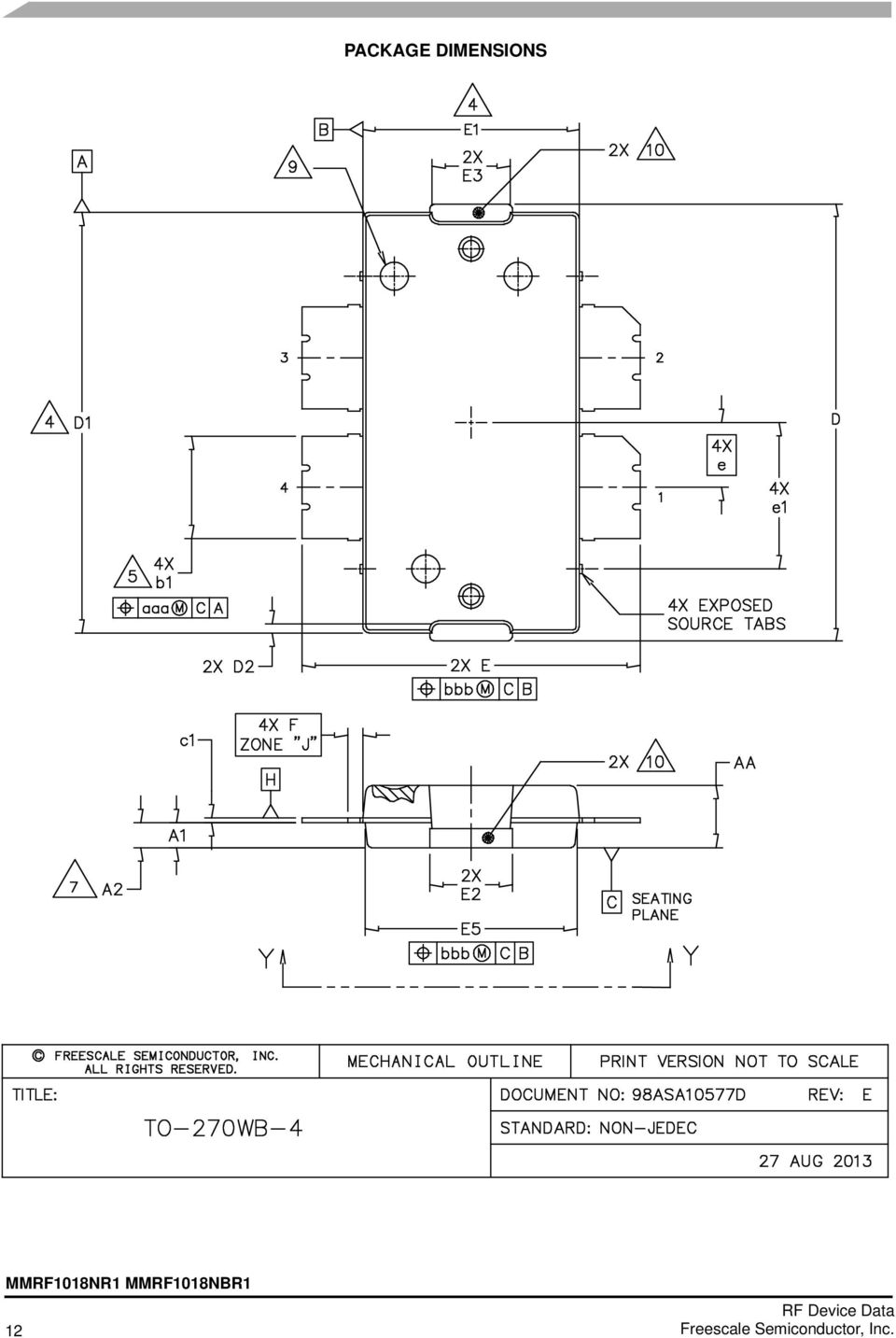
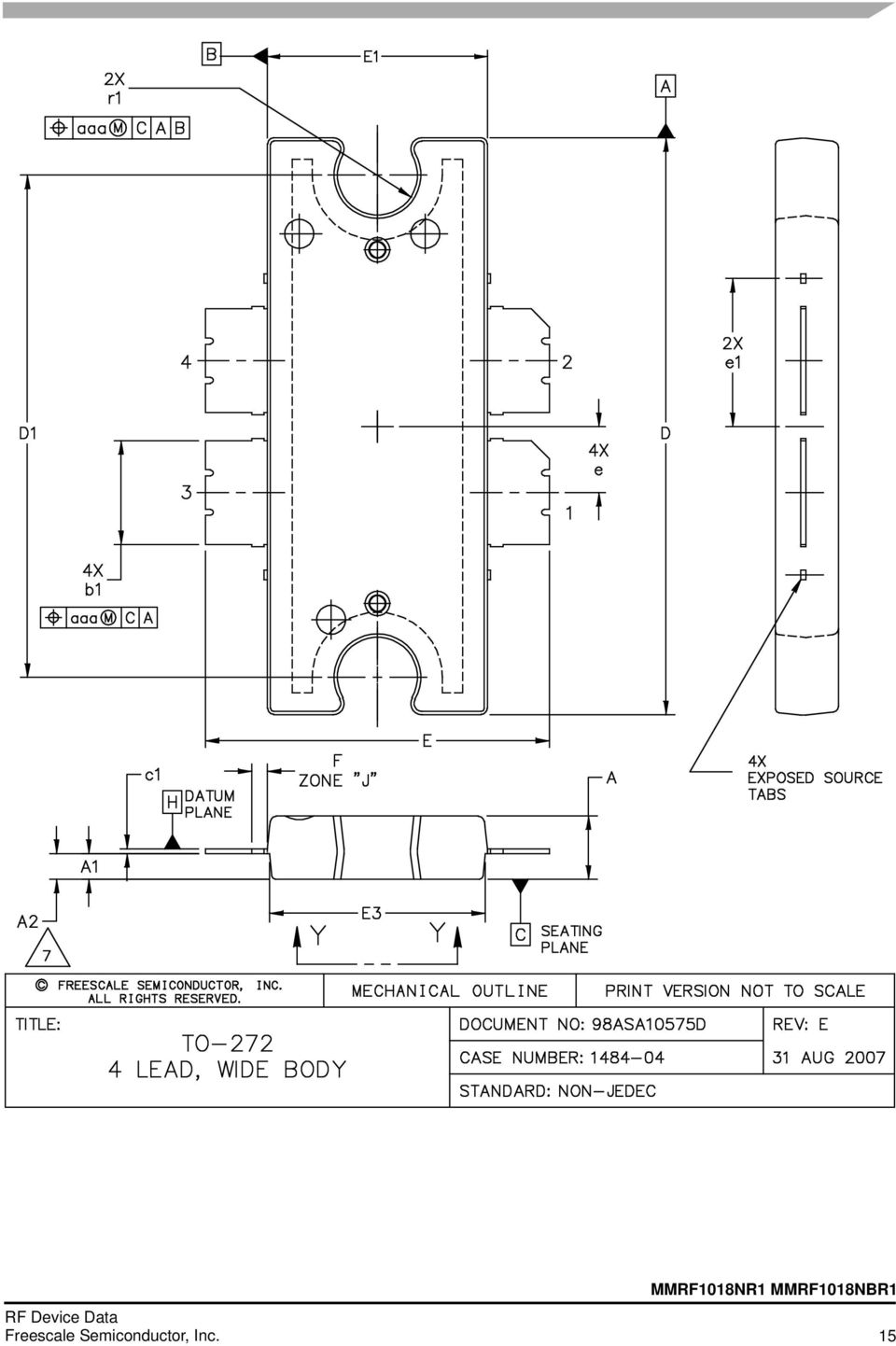
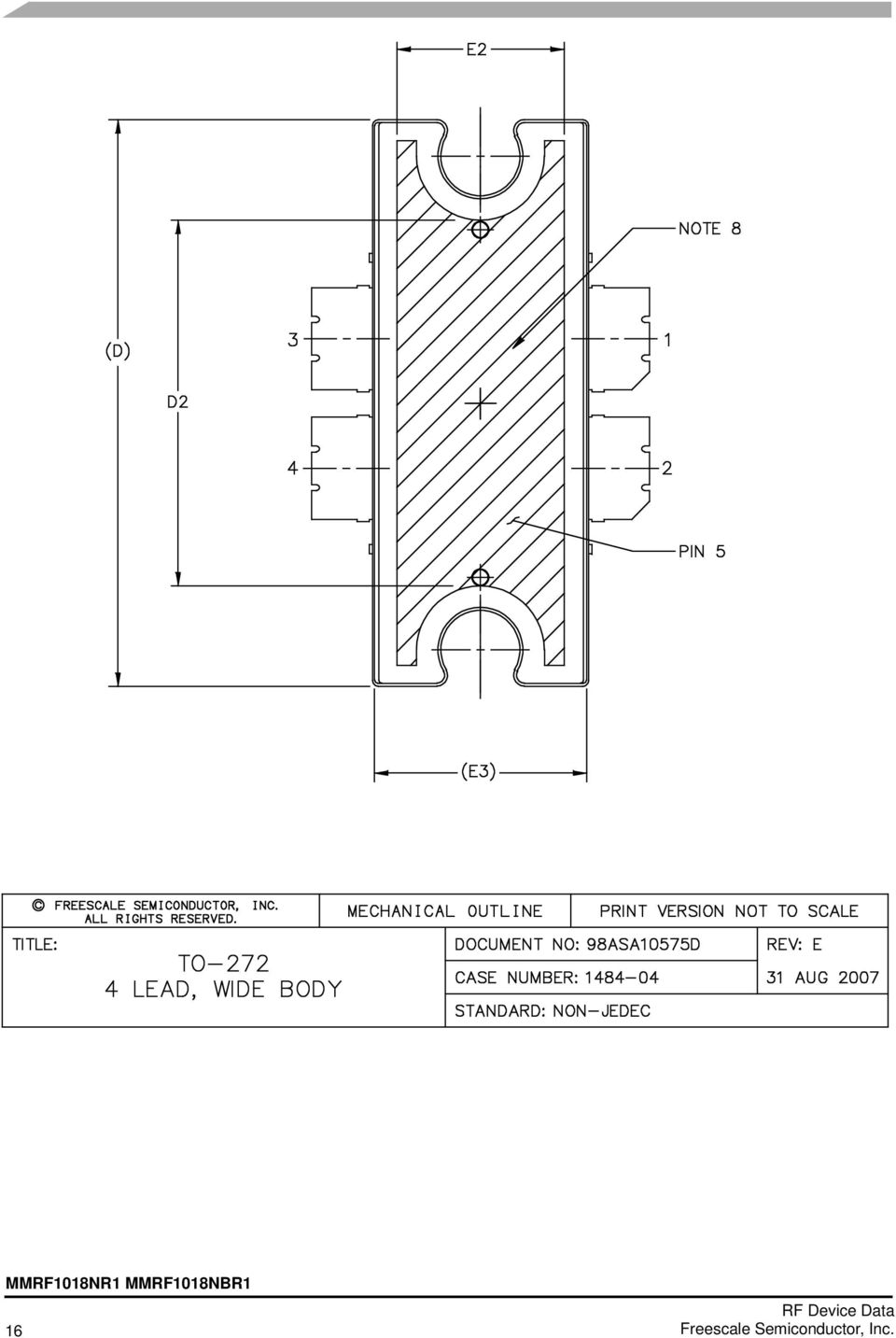
1 Freescale Semiconductor Technical Data RF Power LDMOS Transistors Enhancement--Mode Lateral MOSFETs These 90 W RF power LDMOS transistors are designed for wideband RF power amplifiers covering the frequency range of 470 to 860 MHz. Typical Performance (Narrowband Test Circuit): V DD =50Vdc,I DQ = 350 ma, 64 QAM, Input Signal PAR = % Probability on CCDF. Document Number: MMRF8N Rev. 0, 7/4 MMRF8NR MMRF8NBR Signal Type P out (W) f (MHz) G ps (db) D (%) ACPR (dbc) DVB--T (8k OFDM) 8 Avg Typical Performance (Broadband Reference Circuit): V DD =50Vdc, I DQ = 450 ma, 64 QAM, Input Signal PAR = % Probability on CCDF. Signal Type P out (W) f (MHz) G ps (db) D (%) Output Signal PAR (db) IMD Shoulder (dbc) DVB--T (8k OFDM) 8 Avg MHz, 90 W, 50 V BROADBAND RF POWER LDMOS TRANSISTORS TO -270WB -4 PLASTIC MMRF8NR Features Capable of Handling : VSWR, All Phase 50 Vdc, 860 MHz, 90 W CW Output Power Characterized with Series Equivalent Large--Signal Impedance Parameters Internally Input Matched for Ease of Use Qualified Up to a Maximum of 50 V DD Operation Integrated ESD Protection Excellent Thermal Stability Greater Negative Gate--Source Voltage Range for Improved Class C Operation 225 C Capable Plastic Package In Tape and Reel. R Suffix = 50 Units, 44 mm Tape Width, 3--inch Reel. Gate A TO -272WB -4 PLASTIC MMRF8NBR PARTS ARE SINGLE -ENDED Drain A Table. Maximum Ratings Rating Symbol Value Unit Gate B Drain B Drain--Source Voltage V DSS --0.5, + Vdc Gate--Source Voltage V GS --6.0, + Vdc Storage Temperature Range T stg to +50 C Case Operating Temperature T C 50 C Operating Junction Temperature (,2) T J 225 C (Top View) Note: Exposed backside of the package is the source terminal for the transistor. Figure. Pin Connections Table 2. Thermal Characteristics Characteristic Symbol Value (2,3) Unit Thermal Resistance, Junction to Case Case Temperature 76 C, 8 W CW, 50 Vdc, I DQ = 350 ma, 860 MHz Case Temperature 80 C, 90 W CW, 50 Vdc, I DQ = 350 ma, 860 MHz R JC C/W. Continuous use at maximum temperature will affect MTTF. 2. MTTF calculator available at Select Software & Tools/Development Tools/Calculators to access MTTF calculators by product. 3. Refer to AN955, Thermal Measurement Methodology of RF Power Amplifiers. Go to Select Documentation/Application Notes -- AN955., 4. All rights reserved.
: V DD =50Vdc, I DQ = 450 ma, 64 QAM, Input Signal PAR = 9.5 db @ 0.0% Probability on CCDF.")
2 Table 3. ESD Protection Characteristics Test Methodology Class Human Body Model (per JESD22--A4) 2 ( V) Machine Model (per EIA/JESD22--A5) B (--400 V) Charge Device Model (per JESD22--C) IV (>00 V) Table 4. Moisture Sensitivity Level Test Methodology Rating Package Peak Temperature Unit Per JESD22--A3, IPC/JEDEC J--STD C Table 5. Electrical Characteristics (T A =25 C unless otherwise noted) Characteristic Symbol Min Typ Max Unit Off Characteristics Gate--Source Leakage Current (V GS =5Vdc,V DS =0Vdc) Drain--Source Breakdown Voltage (I D =50mA,V GS =0Vdc) Zero Gate Voltage Drain Leakage Current (V DS =50Vdc,V GS =0Vdc) Zero Gate Voltage Drain Leakage Current (V DS = 0 Vdc, V GS =0Vdc) On Characteristics Gate Threshold Voltage (V DS =Vdc,I D = 0 Adc) Gate Quiescent Voltage (V DD =50Vdc,I D = 350 madc, Measured in Functional Test) Drain--Source On--Voltage (V GS =Vdc,I D =0.5Adc) Dynamic Characteristics Reverse Transfer Capacitance (V DS =50Vdc 30 MHz, V GS =0Vdc) Output Capacitance (V DS =50Vdc 30 MHz, V GS =0Vdc) Input Capacitance () (V DS =50Vdc,V GS =0Vdc 30 MHz) I GSS 0.5 Adc V (BR)DSS Vdc I DSS Adc I DSS Adc V GS(th) Vdc V GS(Q) Vdc V DS(on) 0.2 Vdc C rss 4 pf C oss 65.4 pf C iss 59 pf Functional Tests (In Freescale DVB--T Narrowband Test Fixture, 50 ohm system) V DD =50Vdc,I DQ = 350 ma, P out =8WAvg., f = 860 MHz, DVB--T (8k OFDM) Single Channel. ACPR measured in 7.6 MHz Channel 4 MHz 4 khz Bandwidth. Power Gain G ps db Drain Efficiency D % Adjacent Channel Power Ratio ACPR dbc Input Return Loss IRL db. Part internally input matched. 2
 Characteristic Symbol Min Typ Max Unit Off Characteristics Gate--Source Leakage Current (V GS =5Vdc,V DS =0Vdc) Drain--Source Breakdown")
3 V BIAS + C R C2 C3 C8 C9 + C V SUPPLY Z8 Z RF INPUT Z C5 C4 R2 Z2 Z3 Z4 Z5 Z6 Z7 C6 C7 DUT Z9 Z2 Z3 C5 Z4 C Z5 C2 Z6 RF OUTPUT Z7 Z8 C4 C3 Z + C6 C7 C8 Z Z2 Z3 Z4 Z5 Z6 Z7 Z8 Z Microstrip Microstrip Microstrip Microstrip Microstrip Microstrip Microstrip Microstrip Microstrip Z, Z Microstrip Z Microstrip Z Microstrip Z Microstrip Z Microstrip Z Microstrip Z Microstrip Z Microstrip Figure 2. MMRF8NR(NBR) 860 MHz Narrowband Test Circuit Schematic Table 6. MMRF8NR(NBR) 860 MHz Narrowband Test Circuit Component Designations and Values Part Description Part Number Manufacturer C 22 F, 35 V Tantalum Capacitor T49X226K035AT Kermet C2, C9, C7 F, 50 V Chip Capacitors GRM55DR6H6KA88L Murata C3, C5, C8, C4, C6 43 pf Chip Capacitors ATC0B430JT500XT ATC C4 6.2 pf Chip Capacitor ATC0B6R2BT500XT ATC C6 2.2 pf Chip Capacitor ATC0B2R2JT500XT ATC C7 9. pf Chip Capacitor ATC0B9RCT500XT ATC C, C8 2 F, 0 V Electrolytic Capacitors EEVFK2A22M Panasonic--ECG C, C5 7.5 pf Chip Capacitors ATC0B7R5CT500XT ATC C2 3.0 pf Chip Capacitor ATC0B3R0CT500XT ATC C3 0.7 pf Chip Capacitor ATC0B0R7BT500XT ATC R k, /4 W Chip Resistor CRCW6KOJNEA Vishay R2, /4 W Chip Resistor CRCW6ROJNEA Vishay PCB 0.030, r =3.5 RF--35 Taconic 3
 860 MHz Narrowband Test Circuit Schematic Table 6.")
4 -- C C C8 C9 R C2 C3 C4 R2 C C4 C5 C6 C7 CUT OUT AREA C5 C2 C3 C6 C7 C8 -- Figure 3. MMRF8NR(NBR) 860 MHz Narrowband Test Circuit Component Layout 4
 860 MHz Narrowband Test")
5 TYPICAL CHARACTERISTICS C, CAPACITANCE (pf) 00 0 Measured with 30 MHz, V GS =0Vdc V DS, DRAIN--SOURCE VOLTAGE (VOLTS) Figure 4. Capacitance versus Drain -Source Voltage C iss C oss C rss G ps, POWER GAIN (db) V DD =50Vdc,I DQ = 350 ma, f = 860 MHz G ps 9 8 D P out, OUTPUT POWER (WATTS) Figure 5. CW Power Gain and Drain Efficiency versus Output Power (Narrowband Test Circuit) D, DRAIN EFFICIENCY (%) P out, OUTPUT POWER (dbm) P3dB = 5.28 dbm (34.3 W) P2dB = 5.06 dbm (27.6 W) PdB = 50.7 dbm (7.5 W) V 45 V 48 7 V DD =50Vdc,I DQ = 350 ma, f = 860 MHz 47 6 V DD =40V P in, INPUT POWER (dbm) Ideal Actual Figure 6. CW Output Power versus Input Power (Narrowband Test Circuit) G ps, POWER GAIN (db) I DQ = 350 ma, f = 860 MHz P out, OUTPUT POWER (WATTS) Figure 7. CW Power Gain versus Output Power (Narrowband Test Circuit) V DD =50Vdc,I DQ = 350 ma, f = 860 MHz T C =--30_C G ps, POWER GAIN (db) T C =--30_C 85_C 25_C G ps D 85_C 25_C D, DRAIN EFFICIENCY (%) 8 P out, OUTPUT POWER (WATTS) Figure 8. CW Power Gain and Drain Efficiency versus Output Power (Narrowband Test Circuit) 5
 PdB = 50.7 dbm (7.")
6 TYPICAL CHARACTERISTICS TWO -TONE (NARROWBAND TEST CIRCUIT) IMD, INTERMODULATION DISTORTION (dbc) V DD =50Vdc,I DQ = 350 ma, f = 854 MHz f2 = 860 MHz, Two--Tone Measurements 3rd Order 5th Order 7th Order 0 0 IMD, INTERMODULATION DISTORTION (dbc) V DD =50Vdc,P out = 90 W (PEP), I DQ = 350 ma f = 860 MHz, Two--Tone Measurements 3rd Order 5th Order 7th Order 90 P out, OUTPUT POWER (WATTS) PEP TWO--TONE SPACING (MHz) Figure 9. Intermodulation Distortion Products versus Output Power Figure. Intermodulation Distortion Products versus Two -Tone Spacing G ps, POWER GAIN (db) I DQ = 450 ma 350 ma 300 ma 250 ma V DD = 50 Vdc, f = 854 MHz, f2 = 860 MHz Two--Tone Measurements, 6 MHz Tone Spacing 0 0 P out, OUTPUT POWER (WATTS) PEP Figure. Two -Tone Power Gain versus Output Power IMD, THIRD ORDER INTERMODULATION DISTORTION (dbc) V DD = 50 Vdc, f = 854 MHz, f2 = 860 MHz Two--Tone Measurements, 6 MHz Tone Spacing I DQ = 250 ma 350 ma 300 ma 450 ma P out, OUTPUT POWER (WATTS) PEP 0 Figure 2. Third Order Intermodulation Distortion versus Output Power 0 6
 23.5 23")
7 TYPICAL CHARACTERISTICS DVB -T (8k OFDM) PROBABILITY (%) DVB--T (8k OFDM) 64 QAM Data Carrier Modulation 5 Symbols (db) kHzBW 7.6 MHz ACPR Measured at 4 MHz Offset from Center Frequency 4kHzBW DVB--T (8k OFDM) 64 QAM Data Carrier Modulation, 5 Symbols PEAK--TO--AVERAGE (db) f, FREQUENCY (MHz) Figure 3. Single -Carrier DVB -T (8k OFDM) Figure 4. DVB -T (8k OFDM) Spectrum G ps, POWER GAIN (db) I DQ = 450 ma 350 ma 300 ma 250 ma 2 V DD = 50 Vdc, f = 860 MHz DVB--T (8k OFDM), 64 QAM Data Carrier Modulation, 5 Symbols.5 40 P out, OUTPUT POWER (WATTS) AVG. Figure 5. Single -Carrier DVB -T (8k OFDM) Power Gain versus Output Power (Narrowband Test Circuit) ACPR, ADJACENT CHANNEL POWER RATIO (dbc) V DD = 50 Vdc, f = 860 MHz DVB--T (8k OFDM), 64 QAM Data Carrier Modulation, 5 Symbols I DQ = 250 ma 300 ma ma ma P out, OUTPUT POWER (WATTS) AVG. Figure 6. Single -Carrier DVB -T (8k OFDM) ACPR versus Output Power (Narrowband Test Circuit) G ps, POWER GAIN (db) D, DRAIN EFFICIENCY (%) V DD =50Vdc,I DQ = 350 ma --30_C f = 860 MHz, DVB--T (8k OFDM) QAM Data Carrier Modulation Symbols D 25_C _C G ps 85_C T C =--30_C 25_C ACPR P out, OUTPUT POWER (WATTS) AVG. Figure 7. Single -Carrier DVB -T (8k OFDM) Drain Efficiency, Power Gain and ACPR versus Output Power (Narrowband Test Circuit) ACPR, ADJACENT CHANNEL POWER RATIO (dbc) 7
 Figure 4. DVB -T (8k OFDM) Spectrum G ps, POWER GAIN (db) 23 22.5 22 2.")
8 TYPICAL CHARACTERISTICS 9 8 V DD =50Vdc P out =8WAvg. D = 28.5% MTTF (HOURS) T J, JUNCTION TEMPERATURE ( C) MTTF calculator available at Select Software & Tools/Development Tools/Calculators to access MTTF calculators by product. 250 Figure 8. MTTF versus Junction Temperature - CW f MHz V DD =50Vdc,I DQ = 350 ma, P out = 8 W Average Z source Z load j j3.98 Z source = Test circuit impedance as measured from gate to ground. Z load = Test circuit impedance as measured from drain to ground. Input Matching Network Device Under Test Output Matching Network Z source Z load Figure 9. Series Equivalent Source and Load Impedance (Narrowband Test Circuit) 8

9 MHz BROADBAND REFERENCE CIRCUIT V DD =50Vdc,I DQ = 450 ma, Channel Bandwidth = 8 MHz, Input Signal PAR = % Probability on CCDF. Signal Type P out (W) f (MHz) G ps (db) D (%) Output PAR (db) IMD Shoulder (dbc) DVB--T (8k OFDM) 4.5 Avg Avg Avg R V DD V GG C4 C5 C6 C7 C3 C C4 C5 C7 C Q C9 C2 C2 C6 C8 C C3 C8 C9 C Figure. MMRF8NR(NBR) MHz Broadband 2 3 Compact Reference Circuit Component Layout 9

10 MHz BROADBAND REFERENCE CIRCUIT Table 7. MMRF8NR(NBR) MHz Broadband 2 3 Reference Circuit Component Designations and Values Part Description Part Number Manufacturer C, C2 0 pf Chip Capacitors ATC0BJT500XT ATC C2.8 pf Chip Capacitor ATC0BR8BT500XT ATC C3 6.2 pf Chip Capacitor ATC0B6R2BT500XT ATC C4, C5, C6 3 pf Chip Capacitors ATC0B30JT500XT ATC C7, C8, C 2.2 pf Chip Capacitors ATC0B2R2JT500XT ATC C9 5 pf Chip Capacitor ATC0B50JT500XT ATC C 3.9 pf Chip Capacitor ATC0B3R9CT500XT ATC C3 47 F, 6 V Tantalum Capacitor T49D476K06AS Kemet C4, C7, C9 2.2 F, 0 V Chip Capacitors C3225X7R2A225KT TDK C5, C6, C8 2 pf Chip Capacitors ATC0B22JT0XT ATC C 470 F, 63 V Electrolytic Capacitor MCGPR63V477M3X26--RH Multicomp Q RF High Power Transistor MRF6V3090NBR Freescale R, /4 W Chip Resistor CRCW6RJ Vishay PCB Rogers RO4350B, 0.030, r =3.66 MTL

11 TYPICAL CHARACTERISTICS MHz BROADBAND REFERENCE CIRCUIT G ps, POWER GAIN (db) V DD =50Vdc,I DQ = 450 ma, DVB--T (8k OFDM) 64 QAM Data Carrier Modulation, 5 Symbols G ps D P out =4.5W 9W 8 W 8 W 9W 4.5 W D, DRAIN EFFICIENCY (%) f, FREQUENCY (MHz) Figure 2. Single -Carrier DVB -T (8k OFDM) Power Gain and Drain Efficiency versus Frequency (Broadband Reference Circuit) OUTPUT PAR (db) V DD =50Vdc,I DQ = 450 ma, DVB--T (8k OFDM) 64 QAM Data Carrier Modulation, 5 Symbols PAR P out =4.5W --30 IMD () 8 W W W f, FREQUENCY (MHz) () Intermodulation distortion shoulder measurement made using delta marker at 4.2 MHz offset from center frequency. Figure 22. Single -Carrier DVB -T (8k OFDM) Output PAR and IMD Shoulder versus Frequency (Broadband Reference Circuit) 9W 8 W IMD, INTERMODULATION DISTORTION SHOULDER (dbc) G ps, POWER GAIN (db) V DD =50Vdc,I DQ = 450 ma Pulse Width = 0 sec, % Duty Cycle 6 MHz 740 MHz 860 MHz 470 MHz G ps D 860 MHz 70 6 MHz MHz MHz D DRAIN EFFICIENCY (%) P out, OUTPUT POWER (WATTS) PEAK Figure 23. Power Gain and Drain Efficiency versus Output Power (Broadband Reference Circuit)
 8 W --35 9W --40 4.")
12 PACKAGE DIMENSIONS 2
13 3
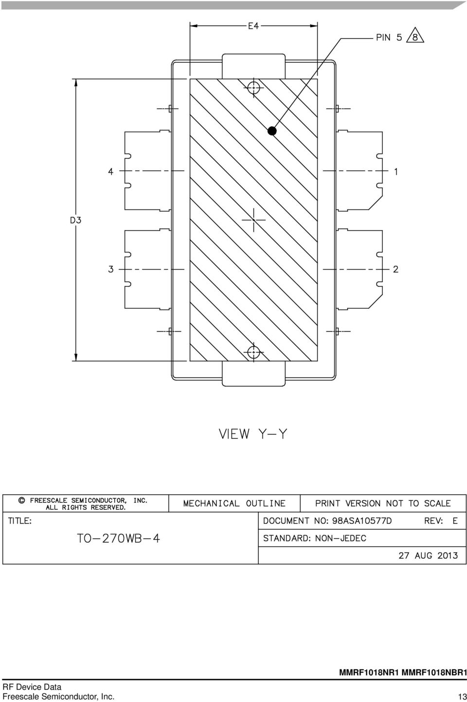
14 4

15 5
16 6
17 7

18 PRODUCT DOCUMENTATION AND SOFTWARE Refer to the following resources to aid your design process. Application Notes AN907: Solder Reflow Attach Method for High Power RF Devices in Over--Molded Plastic Packages AN955: Thermal Measurement Methodology of RF Power Amplifiers AN3263: Bolt Down Mounting Method for High Power RF Transistors and RFICs in Over--Molded Plastic Packages AN3789: Clamping of High Power RF Transistors and RFICs in Over--Molded Plastic Packages Engineering Bulletins EB22: Using Data Sheet Impedances for RF LDMOS Devices Software Electromigration MTTF Calculator For Software, do a Part Number search at and select the Part Number link. Go to the Software & Tools tab on the part s Product Summary page to download the respective tool. REVISION HISTORY The following table summarizes revisions to this document. Revision Date Description 0 July 4 Initial Release of Data Sheet 8

19 How to Reach Us: Home Page: freescale.com Web Support: freescale.com/support Information in this document is provided solely to enable system and software implementers to use Freescale products. There are no express or implied copyright licenses granted hereunder to design or fabricate any integrated circuits based on the information in this document. Freescale reserves the right to make changes without further notice to any products herein. Freescale makes no warranty, representation, or guarantee regarding the suitability of its products for any particular purpose, nor does Freescale assume any liability arising out of the application or use of any product or circuit, and specifically disclaims any and all liability, including without limitation consequential or incidental damages. Typical parameters that may be provided in Freescale data sheets and/or specifications can and do vary in different applications, and actual performance may vary over time. All operating parameters, including typicals, must be validated for each customer application by customer s technical experts. Freescale does not convey any license under its patent rights nor the rights of others. Freescale sells products pursuant to standard terms and conditions of sale, which can be found at the following address: freescale.com/salestermsandconditions. Freescale and the Freescale logo are trademarks of, Reg. U.S. Pat. & Tm. Off. All other product or service names are the property of their respective owners. E 4 Document RF Device Number: DataMMRF8N Rev. Freescale 0, 7/4Semiconductor, Inc. 9

RF Power LDMOS Transistor High Ruggedness N--Channel Enhancement--Mode Lateral MOSFET
 Freescale Semiconductor Technical Data RF Power LDMOS Transistor High Ruggedness N--Channel Enhancement--Mode Lateral MOSFET RF power transistor suitable for both narrowband and broadband CW or pulse applications
RF Power Field Effect Transistors N--Channel Enhancement--Mode Lateral MOSFETs
 Technical Data RF Power Field Effect Transistors N--Channel Enhancement--Mode Lateral MOSFETs Designed for CDMA base station applications with frequencies from 1930 to 1990 MHz. Can be used in Class AB
RF Power Field Effect Transistors N- Channel Enhancement- Mode Lateral MOSFETs
 Technical Data RF Power Field Effect Transistors N- Channel Enhancement- Mode Lateral MOSFETs Designed for GSM and GSM EDGE base station applications with frequencies from 864 to 894 MHz. Suitable for
NOT RECOMMENDED FOR NEW DESIGN
 Technical Data RF Power Field Effect Transistor N-Channel Enhancement-Mode Lateral MOSFET Designed for broadband commercial and industrial applications with frequencies up to 1000 MHz. The high gain and
NOT RECOMMENDED FOR NEW DESIGN
 Technical Data RF Power Field Effect Transistor N-Channel Enhancement-Mode Lateral MOSFET Designed for broadband commercial and industrial applications with frequencies up to 00 MHz. The high gain and
NOT RECOMMENDED FOR NEW DESIGN
 Technical Data RF Power Field Effect Transistor N- Channel Enhancement- Mode Lateral MOSFET Designed for broadband commercial and industrial applications with frequencies up to 00 MHz. The high gain and
RF Power Field Effect Transistors High Ruggedness N--Channel Enhancement--Mode Lateral MOSFETs
 Technical Data RF Power Field Effect Transistors High Ruggedness N--Channel Enhancement--Mode Lateral MOSFETs These high ruggedness devices are designed for use in high VSWR industrial (including laser
Heterojunction Bipolar Transistor Technology (InGaP HBT) Broadband High Linearity Amplifier
 Broadband High Linearity Amplifier") Freescale Semiconductor Technical Data Heterojunction Bipolar Transistor Technology (InGaP HBT) Broadband High Linearity Amplifier The is a general purpose amplifier that is input and output internally
Freescale Semiconductor Technical Data Heterojunction Bipolar Transistor Technology (InGaP HBT) Broadband High Linearity Amplifier The is a general purpose amplifier that is input and output internally
RF Power LDMOS Transistors High Ruggedness N--Channel Enhancement--Mode Lateral MOSFETs
 Freescale Semiconductor Technical Data RF Power LDMOS Transistors High Ruggedness N--Channel Enhancement--Mode Lateral MOSFETs RF power transistors designed for both narrowband and broadband ISM, broadcast
UGF09030. 30W, 1 GHz, 26V Broadband RF Power N-Channel Enhancement-Mode Lateral MOSFET
 30W, 1 GHz, 26V Broadband RF Power N-Channel Enhancement-Mode Lateral MOSFET Designed for base station applications in the frequency band 800MHz to 1000MHz. Rated with a minimum output power of 30W, it
Simple Method of Changing the Frequency Range of a Power Amplifier Circuit
 Freescale Semiconductor Application Note AN4859 Rev. 0, 8/2014 Simple Method of Changing the Frequency Range of a Power Amplifier Circuit Amplifier designers often face the challenge of modifying an existing
BLL6G1214L-250. 1. Product profile. LDMOS L-band radar power transistor. 1.1 General description. 1.2 Features and benefits. 1.
 BLL6G1214L-25 Rev. 1 16 February 212 Preliminary data sheet 1. Product profile 1.1 General description 25 W LDMOS power transistor intended for L-band radar applications in the 1.2 GHz to 1.4 GHz range.
TSM2N7002K 60V N-Channel MOSFET
 SOT-23 SOT-323 Pin Definition: 1. Gate 2. Source 3. Drain PRODUCT SUMMARY V DS (V) R DS(on) (Ω) I D (ma) 5 @ V GS = 10V 100 60 5.5 @ V GS = 5V 100 Features Low On-Resistance ESD Protection High Speed Switching
2N5460, 2N5461, 2N5462. JFET Amplifier. P Channel Depletion. Pb Free Packages are Available* Features. http://onsemi.com MAXIMUM RATINGS
 2N546, 2N5461, JFET Amplifier PChannel Depletion Features PbFree Packages are Available* MAXIMUM RATINGS Rating Symbol Value Unit Drain Gate Voltage V DG 4 Vdc Reverse Gate Source Voltage V GSR 4 Vdc Forward
NTMS4920NR2G. Power MOSFET 30 V, 17 A, N Channel, SO 8 Features
 NTMS9N Power MOSFET 3 V, 7 A, N Channel, SO Features Low R DS(on) to Minimize Conduction Losses Low Capacitance to Minimize Driver Losses Optimized Gate Charge to Minimize Switching Losses These Devices
MMBF4391LT1G, SMMBF4391LT1G, MMBF4392LT1G, MMBF4393LT1G. JFET Switching Transistors. N Channel
 LT1G, SLT1G, LT1G, LT1G JFET Switching Transistors NChannel Features S Prefix for Automotive and Other Applications Requiring Unique Site and Control Change Requirements; AECQ1 Qualified and PPAP Capable
N-Channel 60-V (D-S), 175 C MOSFET
, 175 C MOSFET") N-Channel 6-V (D-S), 75 C MOSFET SUP/SUB7N6-4 V (BR)DSS (V) r DS(on) ( ) (A) 6.4 7 a TO-22AB D TO-263 DRAIN connected to TAB G G D S Top View SUP7N6-4 G D S Top View SUB7N6-4 S N-Channel MOSFET Parameter
N-Channel 6-V (D-S), 75 C MOSFET SUP/SUB7N6-4 V (BR)DSS (V) r DS(on) ( ) (A) 6.4 7 a TO-22AB D TO-263 DRAIN connected to TAB G G D S Top View SUP7N6-4 G D S Top View SUB7N6-4 S N-Channel MOSFET Parameter
N-Channel 20-V (D-S) 175 C MOSFET
 175 C MOSFET") N-Channel -V (D-S) 75 C MOSFET SUD7N-4P PRODUCT SUMMARY V DS (V) r DS(on) ( ) (A) a.37 @ V GS = V 37.6 @ V GS = 4.5 V 9 TO-5 D FEATURES TrenchFET Power MOSFET 75 C Junction Temperature PWM Optimized for
N-Channel -V (D-S) 75 C MOSFET SUD7N-4P PRODUCT SUMMARY V DS (V) r DS(on) ( ) (A) a.37 @ V GS = V 37.6 @ V GS = 4.5 V 9 TO-5 D FEATURES TrenchFET Power MOSFET 75 C Junction Temperature PWM Optimized for
TQP0103 15 W, DC to 4 GHz, GaN Power Transistor
 Applications W-CDMA / LTE Macrocell Base Station Driver Microcell Base Station Small Cell Active Antenna General Purpose Applications 20 Pin 3x4mm QFN Product Features Functional Block Diagram Operating
DISCRETE SEMICONDUCTORS DATA SHEET. BLF244 VHF power MOS transistor
 DISCRETE SEMICONDUCTORS DATA SHEET September 1992 FEATURES High power gain Low noise figure Easy power control Good thermal stability Withstands full load mismatch Gold metallization ensures excellent
DISCRETE SEMICONDUCTORS DATA SHEET M3D060. BLF177 HF/VHF power MOS transistor. Product specification Supersedes data of 1998 Jul 02.
 DISCRETE SEMICONDUCTORS DATA SHEET M3D6 Supersedes data of 1998 Jul 2 23 Jul 21 FEATURES High power gain Low intermodulation distortion Easy power control Good thermal stability Withstands full load mismatch.
P D 215 1.25 Operating Junction Temperature T J 200 C Storage Temperature Range T stg 65 to +150 C
 SEMICONDUCTOR TECHNICAL DATA Order this document by /D The RF Line The is designed for output stages in band IV and V TV transmitter amplifiers. It incorporates high value emitter ballast resistors, gold
STN3NF06L. N-channel 60 V, 0.07 Ω, 4 A, SOT-223 STripFET II Power MOSFET. Features. Application. Description
 N-channel 60 V, 0.07 Ω, 4 A, SOT-223 STripFET II Power MOSFET Features Type V DSS (@Tjmax) Exceptional dv/dt capability Avalanche rugged technology 100% avalanche tested R DS(on) max STN3NF06L 60 V < 0.1
N-Channel 60-V (D-S) MOSFET
 MOSFET") 7/7, VQJ/P, BS7 -Channel 6-V (D-S) MOSFET Part umber V (BR)DSS Min (V) r DS(on) Max ( ) V GS(th) (V) I D (A) 7 5 @ V GS = V.8 to. 7 7.5 @ V GS = V to.5.5 VQJ 6 5.5 @ V GS = V.8 to.5.5 VQP 5.5 @ V GS =
7/7, VQJ/P, BS7 -Channel 6-V (D-S) MOSFET Part umber V (BR)DSS Min (V) r DS(on) Max ( ) V GS(th) (V) I D (A) 7 5 @ V GS = V.8 to. 7 7.5 @ V GS = V to.5.5 VQJ 6 5.5 @ V GS = V.8 to.5.5 VQP 5.5 @ V GS =
N-Channel 40-V (D-S) 175 C MOSFET
 175 C MOSFET") N-Channel 4-V (D-S) 75 C MOSFET SUP/SUB85N4-4 PRODUCT SUMMARY V (BR)DSS (V) r DS(on) ( ) (A) 4.4 @ V GS = V 85 a TO-22AB D TO-263 G DRAIN connected to TAB G D S Top View Ordering Information SUP85N4-4
N-Channel 4-V (D-S) 75 C MOSFET SUP/SUB85N4-4 PRODUCT SUMMARY V (BR)DSS (V) r DS(on) ( ) (A) 4.4 @ V GS = V 85 a TO-22AB D TO-263 G DRAIN connected to TAB G D S Top View Ordering Information SUP85N4-4
Features. Symbol JEDEC TO-220AB
 Data Sheet June 1999 File Number 2253.2 3A, 5V,.4 Ohm, N-Channel Power MOSFET This is an N-Channel enhancement mode silicon gate power field effect transistor designed for applications such as switching
STP80NF55-08 STB80NF55-08 STB80NF55-08-1 N-CHANNEL 55V - 0.0065 Ω - 80A D2PAK/I2PAK/TO-220 STripFET II POWER MOSFET
 STP80NF55-08 STB80NF55-08 STB80NF55-08-1 N-CHANNEL 55V - 0.0065 Ω - 80A D2PAK/I2PAK/TO-220 STripFET II POWER MOSFET TYPE V DSS R DS(on) I D STB80NF55-08/-1 STP80NF55-08 55 V 55 V
TSM020N03PQ56 30V N-Channel MOSFET
 PDFN56 Pin Definition: 1. Source 8. Drain 2. Source 7. Drain 3. Source 6. Drain 4. Gate 5. Drain Key Parameter Performance Parameter Value Unit V DS 30 V R DS(on) (max) V GS = 10V 2 V GS = 4.5V 3 mω Q
STP62NS04Z N-CHANNEL CLAMPED 12.5mΩ - 62A TO-220 FULLY PROTECTED MESH OVERLAY MOSFET
 N-CHANNEL CLAMPED 12.5mΩ - 62A TO-220 FULLY PROTECTED MESH OVERLAY MOSFET TYPE V DSS R DS(on) I D STP62NS04Z CLAMPED
TGF3015-SM. Applications. Product Features. Functional Block Diagram. General Description. Pin Configuration
 Applications Military radar Civilian radar Land mobile and military radio communications Test instrumentation Wideband or narrowband amplifiers Jammers Product Features Functional Block Diagram Frequency:
Features 1.7 A, 20 V. R DS(ON) Symbol Parameter Ratings Units
 Symbol Parameter Ratings Units") N-Channel.5V Specified PowerTrench TM MOSFET April 999 General Description This N-Channel.5V specified MOSFET is produced using Fairchild Semiconductor's advanced PowerTrench process that has been especially
N-Channel.5V Specified PowerTrench TM MOSFET April 999 General Description This N-Channel.5V specified MOSFET is produced using Fairchild Semiconductor's advanced PowerTrench process that has been especially
Power MOSFET FEATURES. IRFZ44PbF SiHFZ44-E3 IRFZ44 SiHFZ44 T C = 25 C
 Power MOSFET PRODUCT SUMMARY (V) 60 R DS(on) (Ω) V GS = 10 V 0.028 Q g (Max.) (nc) 67 Q gs (nc) 18 Q gd (nc) 25 Configuration Single FEATURES Dynamic dv/dt Rating 175 C Operating Temperature Fast Switching
MITSUBISHI RF MOSFET MODULE RA07H4047M
 MITSUBISHI RF MOSFET MODULE RA7H7M RoHS Compliance,-7MHz 7W.V, Stage Amp. For PORTABLE RADIO DESCRIPTION The RA7H7M is a 7-watt RF MOSFET Amplifier Module for.-volt portable radios that operate in the
Features. Description. Table 1. Device summary. Order code Marking Package Packing. STP110N8F6 110N8F6 TO-220 Tube
 N-channel 80 V, 0.0056 Ω typ.,110 A, STripFET F6 Power MOSFET in a TO-220 package Features Datasheet - production data Order code V DS R DS(on)max I D P TOT TAB STP110N8F6 80 V 0.0065 Ω 110 A 200 W TO-220
N-channel enhancement mode TrenchMOS transistor
 FEATURES SYMBOL QUICK REFERENCE DATA Trench technology d V DSS = V Low on-state resistance Fast switching I D = A High thermal cycling performance Low thermal resistance R DS(ON) mω (V GS = V) g s R DS(ON)
P-Channel 1.25-W, 1.8-V (G-S) MOSFET
 MOSFET") Si5DS P-Channel.5-W,.-V (G-S) MOSFET PRODUCT SUMMARY V DS (V) R DS(on) (Ω) I D (A).5 at V GS = -.5 V ±.5 -.7 at V GS = -.5 V ±. at V GS = -. V ± FEATURES Halogen-free According to IEC 9-- Available TrenchFET
Si5DS P-Channel.5-W,.-V (G-S) MOSFET PRODUCT SUMMARY V DS (V) R DS(on) (Ω) I D (A).5 at V GS = -.5 V ±.5 -.7 at V GS = -.5 V ±. at V GS = -. V ± FEATURES Halogen-free According to IEC 9-- Available TrenchFET
OptiMOS Power-Transistor Product Summary
 OptiMOS Power-Transistor Product Summary V DS 55 V R DS(on),max 4) 35 mω Features Dual N-channel Logic Level - Enhancement mode AEC Q11 qualified I D 2 A PG-TDSON-8-4 MSL1 up to 26 C peak reflow 175 C
SIPMOS Small-Signal-Transistor
 SIPMOS Small-Signal-Transistor Features N-channel Depletion mode dv /dt rated Product Summary V DS V R DS(on),max 3.5 Ω I DSS,min.4 A Available with V GS(th) indicator on reel Pb-free lead plating; RoHS
A 1 to 2 GHz, 50 Watt Push-Pull Power Amplifier Using SiC MESFETs. high RF power. densities and cor- capacitances per watt.
 From June 2006 High Frequency Electronics Copyright 2006 Summit Technical Media A 1 to 2 GHz, 50 Watt Push-Pull Power Amplifier Using SiC MESFETs By Raymond S. Pengelly and Carl W. Janke Cree, Inc. Because
STB4NK60Z, STB4NK60Z-1, STD4NK60Z STD4NK60Z-1, STP4NK60Z,STP4NK60ZFP
 STB4NK60Z, STB4NK60Z-1, STD4NK60Z STD4NK60Z-1, STP4NK60Z,STP4NK60ZFP N-channel 600 V - 1.76 Ω - 4 A SuperMESH Power MOSFET DPAK - D 2 PAK - IPAK - I 2 PAK - TO-220 - TO-220FP Features Type V DSS R DS(on)
STP55NF06L STB55NF06L - STB55NF06L-1
 General features STP55NF06L STB55NF06L - STB55NF06L-1 N-channel 60V - 0.014Ω - 55A TO-220/D 2 PAK/I 2 PAK STripFET II Power MOSFET Type V DSS R DS(on) I D STP55NF06L 60V
SSM3K335R SSM3K335R. 1. Applications. 2. Features. 3. Packaging and Pin Configuration. 2012-07-19 Rev.3.0. Silicon N-Channel MOS (U-MOS -H)
") MOSFETs Silicon N-Channel MOS (U-MOS-H) SSM3K335R SSM3K335R 1. Applications Power Management Switches DC-DC Converters 2. Features (1) 4.5-V gate drive voltage. (2) Low drain-source on-resistance : R DS(ON)
MOSFETs Silicon N-Channel MOS (U-MOS-H) SSM3K335R SSM3K335R 1. Applications Power Management Switches DC-DC Converters 2. Features (1) 4.5-V gate drive voltage. (2) Low drain-source on-resistance : R DS(ON)
STW20NM50 N-CHANNEL 550V @ Tjmax - 0.20Ω - 20ATO-247 MDmesh MOSFET
 N-CHANNEL 550V @ Tjmax - 0.20Ω - 20ATO-247 MDmesh MOSFET TYPE V DSS (@Tjmax) R DS(on) I D STW20NM50 550V < 0.25Ω 20 A TYPICAL R DS (on) = 0.20Ω HIGH dv/dt AND AVALANCHE CAPABILITIES 100% AVALANCHE TESTED
P-Channel 20-V (D-S) MOSFET
 MOSFET") Si33DS P-Channel -V (D-S) MOSFET PRODUCT SUMMARY V DS (V) R DS(on) (Ω) I D (A).39 at V GS = -.5 V -.7 -.5 at V GS = -.5 V -..68 at V GS = -.8 V - 3.5 FEATURES Halogen-free According to IEC 69-- Available
Si33DS P-Channel -V (D-S) MOSFET PRODUCT SUMMARY V DS (V) R DS(on) (Ω) I D (A).39 at V GS = -.5 V -.7 -.5 at V GS = -.5 V -..68 at V GS = -.8 V - 3.5 FEATURES Halogen-free According to IEC 69-- Available
STP60NF06. N-channel 60V - 0.014Ω - 60A TO-220 STripFET II Power MOSFET. General features. Description. Internal schematic diagram.
 N-channel 60V - 0.014Ω - 60A TO-220 STripFET II Power MOSFET General features Type V DSS R DS(on) I D STP60NF06 60V
STP10NK60Z/FP, STB10NK60Z/-1 STW10NK60Z N-CHANNEL 600V-0.65Ω-10A TO-220/FP/D 2 PAK/I 2 PAK/TO-247 Zener-Protected SuperMESH Power MOSFET
 STP10NK60Z/FP, STB10NK60Z/-1 STW10NK60Z N-CHANNEL 600V-0.65Ω-10A TO-220/FP/D 2 PAK/I 2 PAK/TO-247 Zener-Protected SuperMESH Power MOSFET TYPE V DSS R DS(on) I D Pw STP10NK60Z STP10NK60ZFP STB10NK60Z STB10NK60Z-1
Power MOSFET FEATURES. IRL540PbF SiHL540-E3 IRL540 SiHL540
 Power MOSFET PRODUCT SUMMARY (V) 100 R DS(on) (Ω) = 5.0 V 0.077 Q g (Max.) (nc) 64 Q gs (nc) 9.4 Q gd (nc) 27 Configuration Single TO220AB G DS ORDERING INFORMATION Package Lead (Pb)free SnPb G D S NChannel
CoolMOS TM Power Transistor
 CoolMOS TM Power Transistor Features New revolutionary high voltage technology Intrinsic fast-recovery body diode Extremely low reverse recovery charge Ultra low gate charge Extreme dv /dt rated Product
MOSFET N-channel enhancement switching transistor IMPORTANT NOTICE. http://www.philips.semiconductors.com use http://www.nxp.com
 Rev. 3 21 November 27 Product data sheet Dear customer, IMPORTANT NOTICE As from October 1st, 26 Philips Semiconductors has a new trade name - NXP Semiconductors, which will be used in future data sheets
BSN20. 1. Description. 2. Features. 3. Applications. 4. Pinning information. N-channel enhancement mode field-effect transistor
 Rev. 3 26 June 2 Product specification. Description in a plastic package using TrenchMOS technology. Product availability: in SOT23. 2. Features TrenchMOS technology Very fast switching Logic level compatible
P-Channel 20 V (D-S) MOSFET
 MOSFET") Si30CDS P-Channel 0 V (D-S) MOSFET MOSFET PRODUCT SUMMARY V DS (V) R DS(on) ( ) I D (A) a Q g (Typ.) - 0 0. at V GS = - 4.5 V - 3. 0.4 at V GS = -.5 V -.7 3.3 nc TO-36 (SOT-3) FEATURES Halogen-free According
Si30CDS P-Channel 0 V (D-S) MOSFET MOSFET PRODUCT SUMMARY V DS (V) R DS(on) ( ) I D (A) a Q g (Typ.) - 0 0. at V GS = - 4.5 V - 3. 0.4 at V GS = -.5 V -.7 3.3 nc TO-36 (SOT-3) FEATURES Halogen-free According
UNISONIC TECHNOLOGIES CO., LTD 50N06 Power MOSFET
 UNISONIC TECHNOLOGIES CO., LTD 50N06 50 Amps, 60 Volts N-CHANNEL POWER MOSFET DESCRIPTION TO-263 TO-25 The UTC 50N06 is three-terminal silicon device with current conduction capability of about 50A, fast
Power MOSFET. IRF510PbF SiHF510-E3 IRF510 SiHF510. PARAMETER SYMBOL LIMIT UNIT Drain-Source Voltage V DS 100 V Gate-Source Voltage V GS ± 20
 Power MOSFET PRODUCT SUMMARY (V) 100 R DS(on) () = 0.54 Q g max. (nc) 8.3 Q gs (nc) 2.3 Q gd (nc) 3.8 Configuration Single D TO220AB G FEATURES Dynamic dv/dt rating Available Repetitive avalanche rated
STP60NF06FP. N-channel 60V - 0.014Ω - 30A TO-220FP STripFET II Power MOSFET. General features. Description. Internal schematic diagram.
 N-channel 60V - 0.014Ω - 30A TO-220FP STripFET II Power MOSFET General features Type V DSS R DS(on) I D STP60NF06FP 60V
BUZ11. 30A, 50V, 0.040 Ohm, N-Channel Power MOSFET. Features. [ /Title (BUZ1 1) /Subject. (30A, 50V, 0.040 Ohm, N- Channel. Ordering Information
 /Subject. (30A, 50V, 0.040 Ohm, N- Channel. Ordering Information") Data Sheet June 1999 File Number 2253.2 [ /Title (BUZ1 1) /Subject (3A, 5V,.4 Ohm, N- Channel Power MOS- FET) /Autho r () /Keywords (Intersil Corporation, N- Channel Power MOS- FET, TO- 22AB ) /Creator
Data Sheet June 1999 File Number 2253.2 [ /Title (BUZ1 1) /Subject (3A, 5V,.4 Ohm, N- Channel Power MOS- FET) /Autho r () /Keywords (Intersil Corporation, N- Channel Power MOS- FET, TO- 22AB ) /Creator
STP10NK80ZFP STP10NK80Z - STW10NK80Z
 STP10NK80ZFP STP10NK80Z - STW10NK80Z N-channel 800V - 0.78Ω - 9A - TO-220/FP-TO-247 Zener-protected supermesh TM MOSFET General features Type V DSS R DS(on) I D Pw STP10NK80Z 800V
Power MOSFET FEATURES. IRF520PbF SiHF520-E3 IRF520 SiHF520. PARAMETER SYMBOL LIMIT UNIT Drain-Source Voltage V DS 100 V Gate-Source Voltage V GS ± 20
 Power MOSFET PRODUCT SUMMARY (V) 100 R DS(on) ( ) = 0.7 Q g (Max.) (nc) 16 Q gs (nc) 4.4 Q gd (nc) 7.7 Configuration Single TO0AB G DS ORDERING INFORMATION Package Lead (Pb)free SnPb G D S NChannel MOSFET
STW34NB20 N-CHANNEL 200V - 0.062 Ω - 34A TO-247 PowerMESH MOSFET
 N-CHANNEL 200V - 0.062 Ω - 34A TO-247 PowerMESH MOSFET Table 1. General Features Figure 1. Package Type V DSS R DS(on) I D STW34NB20 200 V < 0.075 Ω 34 A FEATURES SUMMARY TYPICAL R DS(on) = 0.062 Ω EXTREMELY
2N6387, 2N6388. Plastic Medium-Power Silicon Transistors DARLINGTON NPN SILICON POWER TRANSISTORS 8 AND 10 AMPERES 65 WATTS, 60-80 VOLTS
 2N6388 is a Preferred Device Plastic MediumPower Silicon Transistors These devices are designed for generalpurpose amplifier and lowspeed switching applications. Features High DC Current Gain h FE = 2500
MTD3055VT4. http://onsemi.com. MAXIMUM RATINGS (T C = 25 C unless otherwise noted) MARKING DIAGRAMS ORDERING INFORMATION. R DS(on) TYP 60 V 100 m
 MARKING DIAGRAMS ORDERING INFORMATION. R DS(on) TYP 60 V 100 m") MTD55V Preferred Device Power MOSFET Amps, 6 Volts NChannel This Power MOSFET is designed to withstand high energy in the avalanche and commutation modes. Designed for low voltage, high speed switching
MTD55V Preferred Device Power MOSFET Amps, 6 Volts NChannel This Power MOSFET is designed to withstand high energy in the avalanche and commutation modes. Designed for low voltage, high speed switching
Power MOSFET FEATURES. IRF740PbF SiHF740-E3 IRF740 SiHF740. PARAMETER SYMBOL LIMIT UNIT Drain-Source Voltage V DS 400 V Gate-Source Voltage V GS ± 20
 Power MOSFET PRODUCT SUMMARY (V) 400 R DS(on) (Ω) = 0.55 Q g (Max.) (nc) 63 Q gs (nc) 9.0 Q gd (nc) 3 Configuration Single FEATURES Dynamic dv/dt Rating Repetitive Avalanche Rated Fast Switching Ease of
30 V, single N-channel Trench MOSFET
 SOT883B Rev. 1 11 May 212 Product data sheet 1. Product profile 1.1 General description N-channel enhancement mode Field-Effect Transistor (FET) in a leadless ultra small DFN16B-3 (SOT883B) Surface-Mounted
P-Channel 60 V (D-S) MOSFET
 MOSFET") TP6K P-Channel 6 V (D-S) MOSFET G S PRODUCT SUMMARY V DS (V) R DS(on) ( ) V GS(th) (V) I D (ma) - 6 6 at V GS = - V - to - - 85 TO-6 (SOT-) Top View D Marking Code: 6Kwll 6K = Part Number Code for TP6K
TP6K P-Channel 6 V (D-S) MOSFET G S PRODUCT SUMMARY V DS (V) R DS(on) ( ) V GS(th) (V) I D (ma) - 6 6 at V GS = - V - to - - 85 TO-6 (SOT-) Top View D Marking Code: 6Kwll 6K = Part Number Code for TP6K
SD2942. HF/VHF/UHF RF power N-channel MOSFETs. Features. Description
 HF/VHF/UHF RF power N-channel MOSFETs Features Gold metallization Excellent thermal stability Common source configuration, push pull P OUT = 350 W min. with 15 db gain @ 175 MHz Low R DS(on) Description
Analog Devices Welcomes Hittite Microwave Corporation NO CONTENT ON THE ATTACHED DOCUMENT HAS CHANGED
 Analog Devices Welcomes Hittite Microwave Corporation NO CONTENT ON THE ATTACHED DOCUMENT HAS CHANGED www.analog.com www.hittite.com THIS PAGE INTENTIONALLY LEFT BLANK v2.71 HMC42ST8 / 42ST8E AMPLIFIER,.4-2.2
TPN4R712MD TPN4R712MD. 1. Applications. 2. Features. 3. Packaging and Internal Circuit. 2014-12 2015-04-21 Rev.4.0. Silicon P-Channel MOS (U-MOS )
") MOSFETs Silicon P-Channel MOS (U-MOS) TPN4R712MD TPN4R712MD 1. Applications Lithium-Ion Secondary Batteries Power Management Switches 2. Features (1) Low drain-source on-resistance: R DS(ON) = 3.8 mω (typ.)
MOSFETs Silicon P-Channel MOS (U-MOS) TPN4R712MD TPN4R712MD 1. Applications Lithium-Ion Secondary Batteries Power Management Switches 2. Features (1) Low drain-source on-resistance: R DS(ON) = 3.8 mω (typ.)
Symbol Parameter Value Unit V DS Drain-source Voltage (V GS =0) 50 V V DGR Drain- gate Voltage (R GS =20kΩ) 50 V
 50 V V DGR Drain- gate Voltage (R GS =20kΩ) 50 V") BUZ71A N - CHANNEL 50V - 0.1Ω - 13A TO-220 STripFET POWER MOSFET TYPE V DSS R DS(on) I D BUZ71A 50 V < 0.12 Ω 13 A TYPICAL RDS(on) = 0.1 Ω AVALANCHE RUGGED TECHNOLOGY 100% AVALANCHE TESTED HIGH CURRENT
BUZ71A N - CHANNEL 50V - 0.1Ω - 13A TO-220 STripFET POWER MOSFET TYPE V DSS R DS(on) I D BUZ71A 50 V < 0.12 Ω 13 A TYPICAL RDS(on) = 0.1 Ω AVALANCHE RUGGED TECHNOLOGY 100% AVALANCHE TESTED HIGH CURRENT
OptiMOS 3 Power-Transistor
 Type IPD36N4L G OptiMOS 3 Power-Transistor Features Fast switching MOSFET for SMPS Optimized technology for DC/DC converters Qualified according to JEDEC ) for target applications Product Summary V DS
STP6NK60Z - STP6NK60ZFP STB6NK60Z - STB6NK60Z-1 N-CHANNEL 600V - 1Ω - 6A TO-220/TO-220FP/D 2 PAK/I 2 PAK Zener-Protected SuperMESH Power MOSFET
 STP6NK60Z - STP6NK60ZFP STB6NK60Z - STB6NK60Z-1 N-CHANNEL 600V - 1Ω - 6A TO-220/TO-220FP/D 2 PAK/I 2 PAK Zener-Protected SuperMESH Power MOSFET TYPE V DSS R DS(on) I D Pw STP6NK60Z STP6NK60ZFP STB6NK60Z
2N6056. NPN Darlington Silicon Power Transistor DARLINGTON 8 AMPERE SILICON POWER TRANSISTOR 80 VOLTS, 100 WATTS
 NPN Darlington Silicon Power Transistor The NPN Darlington silicon power transistor is designed for general purpose amplifier and low frequency switching applications. High DC Current Gain h FE = 3000
DATA SHEET. BF245A; BF245B; BF245C N-channel silicon field-effect transistors DISCRETE SEMICONDUCTORS
 DISCRETE SEMICONDUCTORS DATA SHEET N-channel silicon field-effect transistors Supersedes data of April 995 996 Jul BF5A; BF5B; BF5C FEATURES Interchangeability of drain and source connections Frequencies
76-77 GHz RF Transmitter Front-end for W-band Radar Applications
 Freescale Semiconductor Data Sheet Summary for MC33 7-77 GHz RF Transmitter Front-end for W-band Radar Applications The MR2001 is a scalable three package solution for automotive radar modules. The chipset
IRF740 N-CHANNEL 400V - 0.46Ω - 10A TO-220 PowerMESH II MOSFET
 N-CHANNEL 400V - 0.46Ω - 10A TO-220 PowerMESH II MOSFET TYPE V DSS R DS(on) I D IRF740 400 V < 0.55 Ω 10 A TYPICAL R DS (on) = 0.46Ω EXCEPTIONAL dv/dt CAPABILITY 100% AVALANCHE TESTED LOW GATE CHARGE VERY
Power MOSFET FEATURES. IRF610PbF SiHF610-E3 IRF610 SiHF610. PARAMETER SYMBOL LIMIT UNIT Drain-Source Voltage V DS 200 V Gate-Source Voltage V GS ± 20
 Power MOSFET PRODUCT SUMMARY (V) 00 R DS(on) ( ) = 1.5 Q g (Max.) (nc) 8. Q gs (nc) 1.8 Q gd (nc) 4.5 Configuration Single FEATURES Dynamic dv/dt Rating Repetitive Avalanche Rated Fast Switching Ease of
60 V, 360 ma N-channel Trench MOSFET. Symbol Parameter Conditions Min Typ Max Unit V DS drain-source T amb = 25 C - - 60 V
 Rev. 02 29 July 20 Product data sheet 1. Product profile 1.1 General description N-channel enhancement mode Field-Effect Transistor (FET) in a small SOT23 (TO-236AB) Surface-Mounted Device (SMD) plastic
Dual P-Channel 2.5 V (G-S) MOSFET
 MOSFET") Si593DC Dual P-Channel.5 V (G-S) MOSFET PRODUCT SUMMARY V DS (V) R DS(on) (Ω) I D (A).55 at V GS = -.5 V ±.9 -.8 at V GS = - 3.6 V ±.7.6 at V GS = -.5 V ±. FEATURES Halogen-free According to IEC 69-- Definition
Si593DC Dual P-Channel.5 V (G-S) MOSFET PRODUCT SUMMARY V DS (V) R DS(on) (Ω) I D (A).55 at V GS = -.5 V ±.9 -.8 at V GS = - 3.6 V ±.7.6 at V GS = -.5 V ±. FEATURES Halogen-free According to IEC 69-- Definition
Power MOSFET. IRF9520PbF SiHF9520-E3 IRF9520 SiHF9520. PARAMETER SYMBOL LIMIT UNIT Drain-Source Voltage V DS - 100 V Gate-Source Voltage V GS ± 20
 Power MOSFET PRODUCT SUMMARY (V) 100 R DS(on) ( ) = 10 V 0.60 Q g (Max.) (nc) 18 Q gs (nc) 3.0 Q gd (nc) 9.0 Configuration Single TO220AB G DS ORDERING INFORMATION Package Lead (Pb)free SnPb G S D PChannel
STB75NF75 STP75NF75 - STP75NF75FP
 STB75NF75 STP75NF75 - STP75NF75FP N-channel 75V - 0.0095Ω - 80A - TO-220 - TO-220FP - D 2 PAK STripFET II Power MOSFET General features Type V DSS R DS(on) I D STB75NF75 75V
2N3906. General Purpose Transistors. PNP Silicon. Pb Free Packages are Available* http://onsemi.com. Features MAXIMUM RATINGS
 2N396 General Purpose Transistors PNP Silicon Features PbFree Packages are Available* COLLECTOR 3 MAXIMUM RATINGS Rating Symbol Value Unit Collector Emitter Voltage V CEO 4 Vdc Collector Base Voltage V
LM350. 3.0 A, Adjustable Output, Positive Voltage Regulator THREE TERMINAL ADJUSTABLE POSITIVE VOLTAGE REGULATOR
 3. A, able Output, Positive Voltage Regulator The is an adjustable threeterminal positive voltage regulator capable of supplying in excess of 3. A over an output voltage range of 1.2 V to 33 V. This voltage
Power MOSFET FEATURES. IRF740PbF SiHF740-E3 IRF740 SiHF740. PARAMETER SYMBOL LIMIT UNIT Drain-Source Voltage V DS 400 V Gate-Source Voltage V GS ± 20
 Power MOSFET PRODUCT SUMMARY (V) 400 R DS(on) (Ω) = 0.55 Q g (Max.) (nc) 63 Q gs (nc) 9.0 Q gd (nc) 3 Configuration Single FEATURES Dynamic dv/dt Rating Repetitive Avalanche Rated Fast Switching Ease of
OptiMOS TM Power-Transistor
 Type BSC28N6NS OptiMOS TM Power-Transistor Features Optimized for high performance SMPS, e.g. sync. rec. % avalanche tested Superior thermal resistance N-channel Qualified according to JEDEC ) for target
OptiMOS 3 Power-Transistor
 Type IPD6N3L G OptiMOS 3 Power-Transistor Features Fast switching MOSFET for SMPS Optimized technology for DC/DC converters Qualified according to JEDEC 1) for target applications Product Summary V DS
Features. TA=25 o C unless otherwise noted
 NDSAN N-Channel, Logic Level, PowerTrench MOSFET June NDSAN General Description These N-Channel Logic Level MOSFETs are produced using Fairchild Semiconductor s advanced PowerTrench process that has been
50 V, 180 ma P-channel Trench MOSFET. Symbol Parameter Conditions Min Typ Max Unit V DS drain-source voltage T j = 25 C - - -50 V
 SOT23 Rev. 1 23 May 211 Product data sheet 1. Product profile 1.1 General description P-channel enhancement mode Field-Effect Transistor (FET) in a small SOT23 (TO-236AB) Surface-Mounted Device (SMD) plastic
2N3903, 2N3904. General Purpose Transistors. NPN Silicon. Pb Free Packages are Available* Features. http://onsemi.com MAXIMUM RATINGS
 N393, General Purpose Transistors NPN Silicon Features PbFree Packages are Available* MAXIMUM RATINGS Rating Symbol Value Unit CollectorEmitter Voltage V CEO 4 Vdc CollectorBase Voltage V CBO 6 Vdc EmitterBase
A I DM. W/ C V GS Gate-to-Source Voltage ± 20. Thermal Resistance Symbol Parameter Typ. Max. Units
 V DS 2 V V GS Max ± 2 V R DSon) max @V GS = V) 24 m * PD - 9787A HEXFET Power MOSFET R DSon) max @V GS = 4.V) 4 m 6 Micro3 TM SOT-23) Applications) Load System Switch Features and Benefits Features Benefits
Vdc. Vdc. Adc. W W/ C T J, T stg 65 to + 200 C
 2N6284 (NPN); 2N6286, Preferred Device Darlington Complementary Silicon Power Transistors These packages are designed for general purpose amplifier and low frequency switching applications. Features High
SMS7630-061: Surface Mount, 0201 Zero Bias Silicon Schottky Detector Diode
 DATA SHEET SMS7630-061: Surface Mount, 0201 Zero Bias Silicon Schottky Detector Diode Applications Sensitive RF and microwave detector circuits Sampling and mixer circuits High volume wireless systems
A I DM. W/ C V GS Gate-to-Source Voltage ± 12. Thermal Resistance Symbol Parameter Typ. Max. Units
 V DS 2 V V GS Max ±2 V * PD - 973A HEXFET Power MOSFET R DSon) max @V GS = 4.V) 2. m R DSon) max @V GS = 2.V) 27. m 6 Micro3 TM SOT-23) Applications) Load System Switch Features and Benefits Features Benefits
CLA4607-085LF: Surface Mount Limiter Diode
 DATA SHEET CLA4607-085LF: Surface Mount Limiter Diode Applications Low-loss, high-power limiters Receiver protectors Anode (Pin 1) Anode (Pin 3) Features Low thermal resistance: 55 C/W Typical threshold
N-Channel 100 V (D-S) MOSFET
 MOSFET") Si4DS N-Channel V (D-S) MOSFET MOSFET PRODUCT SUMMARY V DS (V) R DS(on) ( ) I D (A) a Q g (Typ.).4 at V GS = V..67 at V GS = 6 V..9 nc.78 at V GS = 4.5 V.7 FEATURES TrenchFET Power MOSFET % R g Tested
Si4DS N-Channel V (D-S) MOSFET MOSFET PRODUCT SUMMARY V DS (V) R DS(on) ( ) I D (A) a Q g (Typ.).4 at V GS = V..67 at V GS = 6 V..9 nc.78 at V GS = 4.5 V.7 FEATURES TrenchFET Power MOSFET % R g Tested
P2N2222ARL1G. Amplifier Transistors. NPN Silicon. These are Pb Free Devices* Features. http://onsemi.com
 Amplifier Transistors NPN Silicon Features These are PbFree Devices* MAXIMUM RATINGS (T A = 25 C unless otherwise noted) Characteristic Symbol Value Unit CollectorEmitter Voltage V CEO 4 CollectorBase
T A = 25 C (Notes 3 & 5) Product Marking Reel size (inches) Tape width (mm) Quantity per reel DMC4040SSD-13 C4040SD 13 12 2,500
 Product Marking Reel size (inches) Tape width (mm) Quantity per reel DMC4040SSD-13 C4040SD 13 12 2,500") Product Line of 4 COMPLEMENTRY PIR ENHNCEMENT MODE MOSFET Product Summary Device (BR)DSS R DS(on) max I D max () T = 25 C (Notes 3 & 5) 25mΩ @ = 1 7.5 Q1 4 4mΩ @ = 4.5 6.2 Features and Benefits Matched
Product Line of 4 COMPLEMENTRY PIR ENHNCEMENT MODE MOSFET Product Summary Device (BR)DSS R DS(on) max I D max () T = 25 C (Notes 3 & 5) 25mΩ @ = 1 7.5 Q1 4 4mΩ @ = 4.5 6.2 Features and Benefits Matched
MASW-000823-12770T. HMIC TM PIN Diode SP2T 13 Watt Switch for TD-SCDMA Applications. Features. Functional Diagram (TOP VIEW)
") Features Exceptional Loss = 0.35 db Avg @ 2025 MHz, 20mA Exceptional Loss = 0.50 db Avg @ 2025 MHz, 20mA Higher - Isolation = 31dB Avg @ 2025 MHz, 20mA Higher RF C.W. Input Power =13 W C.W.(-Ant Port)
Features Exceptional Loss = 0.35 db Avg @ 2025 MHz, 20mA Exceptional Loss = 0.50 db Avg @ 2025 MHz, 20mA Higher - Isolation = 31dB Avg @ 2025 MHz, 20mA Higher RF C.W. Input Power =13 W C.W.(-Ant Port)
Power MOSFET FEATURES. IRF540PbF SiHF540-E3 IRF540 SiHF540. PARAMETER SYMBOL LIMIT UNIT Drain-Source Voltage V DS 100 V Gate-Source Voltage V GS ± 20
 Power MOSFET PRODUCT SUMMARY (V) 100 R DS(on) ( ) = 0.077 Q g (Max.) (nc) 72 Q gs (nc) 11 Q gd (nc) 32 Configuration Single TO220AB G DS ORDERING INFORMATION Package Lead (Pb)free SnPb G D S NChannel MOSFET
2N4401. General Purpose Transistors. NPN Silicon. Pb Free Packages are Available* http://onsemi.com. Features MAXIMUM RATINGS THERMAL CHARACTERISTICS
 General Purpose Transistors NPN Silicon Features PbFree Packages are Available* MAXIMUM RATINGS Rating Symbol Value Unit Collector Emitter Voltage V CEO 4 Vdc Collector Base Voltage V CBO 6 Vdc Emitter