RF Power Field Effect Transistors N--Channel Enhancement--Mode Lateral MOSFETs
|
|
|
- Randell Jonas Murphy
- 9 years ago
- Views:
Transcription
1 Technical Data RF Power Field Effect Transistors N--Channel Enhancement--Mode Lateral MOSFETs Designed for CDMA base station applications with frequencies from 1930 to 1990 MHz. Can be used in Class AB and Class C for all typical cellular base station modulation formats. Typical Single--Carrier W--CDMA Performance: V DD =28Volts,I DQ = 1400 ma, P out = 63 Watts Avg., f = MHz, IQ Magnitude Clipping, Channel Bandwidth = 3.84 MHz, Input Signal PAR = % Probability on CCDF. Power Gain 20 db Drain Efficiency 29% Device Output Signal PAR % Probability on CCDF 5 MHz Offset --33 dbc in 3.84 MHz Channel Bandwidth Capable of Handling 5:1 32 Vdc, 1960 MHz, 190 Watts CW Output Power (3 db Input Overdrive from Rated P out ) Typical P 1 db Compression Point 190 Watts CW Features 100% PAR Tested for Guaranteed Output Power Capability Characterized with Series Equivalent Large--Signal Impedance Parameters Internally Matched for Ease of Use Integrated ESD Protection Greater Negative Gate--Source Voltage Range for Improved Class C Operation Designed for Digital Predistortion Error Correction Systems RoHS Compliant In Tape and Reel. R3 Suffix = 250 Units, 56 mm Tape Width, 13 inch Reel. Document Number: MRF7S19210H Rev. 1, 3/2011 MRF7S19210HR3 MRF7S19210HSR MHz, 63 W AVG., 28 V SINGLE W -CDMA LATERAL N -CHANNEL RF POWER MOSFETs CASE , STYLE 1 NI -780 MRF7S19210HR3 CASE 465A -06, STYLE 1 NI -780S MRF7S19210HSR3 Table 1. Maximum Ratings Rating Symbol Value Unit Drain--Source Voltage V DSS --0.5, +65 Vdc Gate--Source Voltage V GS --6.0, +10 Vdc Operating Voltage V DD 32, +0 Vdc Storage Temperature Range T stg --65 to +150 C Case Operating Temperature T C 150 C Operating Junction Temperature (1,2) T J 225 C Table 2. Thermal Characteristics Characteristic Symbol Value (2,3) Unit Thermal Resistance, Junction to Case Case Temperature 85 C, 190 W CW Case Temperature 79 C, 63 W CW R θjc C/W 1. Continuous use at maximum temperature will affect MTTF. 2. MTTF calculator available at Select Software & Tools/Development Tools/Calculators to access MTTF calculators by product. 3. Refer to AN1955, Thermal Measurement Methodology of RF Power Amplifiers. Go to Select Documentation/Application Notes -- AN1955., Inc., 2008, All rights reserved. 1

2 Table 3. ESD Protection Characteristics Test Methodology Human Body Model (per JESD22--A114) Machine Model (per EIA/JESD22--A115) Charge Device Model (per JESD22--C101) Class 1C (Minimum) A (Minimum) IV (Minimum) Table 4. Electrical Characteristics (T A =25 C unless otherwise noted) Characteristic Symbol Min Typ Max Unit Off Characteristics Zero Gate Voltage Drain Leakage Current (V DS =65Vdc,V GS =0Vdc) Zero Gate Voltage Drain Leakage Current (V DS =28Vdc,V GS =0Vdc) Gate--Source Leakage Current (V GS =5Vdc,V DS =0Vdc) On Characteristics Gate Threshold Voltage (V DS =10Vdc,I D = 513 μadc) Gate Quiescent Voltage (V DS =28Vdc,I D = 1400 madc) Fixture Gate Quiescent Voltage (1) (V DD =28Vdc,I D = 1400 madc, Measured in Functional Test) Drain--Source On--Voltage (V GS =10Vdc,I D =5.13Adc) Dynamic Characteristics (2) Reverse Transfer Capacitance (V DS =28Vdc± 30 1 MHz, V GS =0Vdc) Output Capacitance (V DS =28Vdc± 30 1 MHz, V GS =0Vdc) Input Capacitance (V DS =28Vdc,V GS =0Vdc± 30 1 MHz) I DSS 10 μadc I DSS 1 μadc I GSS 1 μadc V GS(th) Vdc V GS(Q) 2.7 Vdc V GG(Q) Vdc V DS(on) Vdc C rss 2.17 pf C oss 257 pf C iss 508 pf Functional Tests (In Freescale Test Fixture, 50 ohm system) V DD =28Vdc,I DQ = 1400 ma, P out = 63 W Avg., f = MHz, Single--Carrier W--CDMA, IQ Magnitude Clipping, Input Signal PAR = % Probability on CCDF. ACPR measured in 3.84 MHz Channel ±5 MHzOffset. Power Gain G ps db Drain Efficiency η D % Output Peak--to--Average 0.01% Probability on CCDF PAR db Adjacent Channel Power Ratio ACPR dbc Input Return Loss IRL db 1. V GG =2xV GS(Q). Parameter measured on Freescale Test Fixture, due to resistive divider network on the board. Refer to Test Circuit schematic. 2. Part internally matched both on input and output. (continued) 2
 Characteristic Symbol Min Typ Max Unit Off Characteristics Zero Gate Voltage Drain Leakage Current (V DS =65Vdc,V GS =0Vdc) Zero Gate")
3 Table 4. Electrical Characteristics (T A =25 C unless otherwise noted) (continued) Characteristic Symbol Min Typ Max Unit Typical Performances (In Freescale Test Fixture, 50 ohm system) V DD =28Vdc,I DQ = 1400 ma, MHz Bandwidth IMD 160 W PEP, P out where IMD Third Order IMD sym Intermodulation 30 dbc (Delta IMD Third Order Intermodulation between Upper and Lower Sidebands > 2 db) 15 VBW Resonance Point (IMD Third Order Intermodulation Inflection Point) MHz VBW res 50 MHz Gain Flatness in 60 MHz P out =63WAvg. G F 0.9 db Average Deviation from Linear Phase in 60 MHz out = 190 W CW Φ 0.95 Average Group P out = 190 W CW, f = 1960 MHz Delay 2.82 ns Part--to--Part Insertion Phase P out = 190 W CW, f = 1960 MHz, Six Sigma Window Gain Variation over Temperature (--30 C to+85 C) Output Power Variation over Temperature (--30 C to+85 C) Φ 28.9 G db/ C P1dB db/ C 3
 MHz VBW res 50 MHz Gain Flatness in 60 MHz Bandwidth @ P out =63WAvg. G F 0.")
4 R1 Z22 V BIAS R2 C1 C2 C3 Z20 C10 C11 C12 C21 + V SUPPLY R3 RF INPUT Z1 Z2 Z3 Z4 Z5 Z6 Z7 Z8 Z19 Z10 Z9 Z11 Z12 Z13 Z14 Z15 C14 Z16 Z17 C16 Z18 RF OUTPUT C4 C5 C6 Z21 DUT Z23 C13 C15 C17 + C9 C8 C7 C18 C19 C20 C22 Z1 Z2 Z3 Z4 Z5 Z6 Z7 Z8 Z9 Z10 Z11 Z x Microstrip x Microstrip x Microstrip x Microstrip x0.118 Microstrip x0.118 Microstrip x Microstrip x Microstrip x Microstrip x Microstrip x Microstrip x Microstrip Z x Microstrip Z x Microstrip Z x Microstrip Z x Microstrip Z x Microstrip Z x Microstrip Z x Microstrip Z x Microstrip Z x Microstrip Z22, Z x Microstrip PCB Taconic RF35, 0.030, ε r =3.5 Figure 1. MRF7S19210HR3(HSR3) Test Circuit Schematic Table 5. MRF7S19210HR3(HSR3) Test Circuit Component Designations and Values Part Description Part Number Manufacturer C1, C9, C11, C12, C19, C20 10 μf, 50 V Chip Capacitors C5750X5R1H106M TDK C2, C8 100 nf Chip Capacitors 12065C104KAT2A AVX C3, C6, C7, C10, C14, C15, 8.2 pf Chip Capacitors ATC100B8R2BT500XT ATC C18 C4 0.2 pf Chip Capacitor ATC100B0R2BT500XT ATC C5 1.8 pf Chip Capacitor ATC100B1R8BT500XT ATC C pf Chip Capacitor ATC100B0R4BT500XT ATC C16, C pf Chip Capacitors ATC100B0R5BT500XT ATC C21, C μf Electrolytic Capacitors Vishay BC Components R1, R2 10 kω, 1/4 W Chip Resistors WCR120610KFI Welwyn R3 10 Ω, 1/4 W Chip Resistor WCR120610RFI Welwyn 4

5 C1 C2 C10 R1 R2 C3 C11 C12 C21 C4 C5 C6 R3 CUT OUT AREA C13 C14 C15 C16 C17 C8 C7 C19 C20 C22 C9 C18 MRF7S19210H Rev 0 Figure 2. MRF7S19210HR3(HSR3) Test Circuit Component Layout 5
 Test Circuit Component")
6 TYPICAL CHARACTERISTICS G ps η D V DD =28Vdc,P out =63W(Avg.) I DQ = 1400 ma Single--Carrier W--CDMA, 3.84 MHz Channel Bandwidth Input Signal PAR = % Probability on CCDF PARC IRL ACPR f, FREQUENCY (MHz) Figure 3. Output Peak -to -Average Ratio Compression (PARC) Broadband P out = 63 Watts Avg. G ps, POWER GAIN (db) η D, DRAIN EFFICIENCY (%) ACPR (dbc) IRL, INPUT RETURN LOSS (db) PARC (db) G ps, POWER GAIN (db) I DQ = 2100 ma 1750 ma 1050 ma 1400 ma 700 ma V DD =28Vdc f = 1960 MHz P out, OUTPUT POWER (WATTS) CW Figure 4. Power Gain versus Output Power IMD, INTERMODULATION DISTORTION (dbc) V DD =28Vdc,P out = 160 W (PEP), I DQ = 1400 ma Two--Tone Measurements (f1 + f2)/2 = Center Frequency of 1960 MHz IM7--L IM5--U IM5--L IM3--U IM3--L IM7--U TWO--TONE SPACING (MHz) Figure 5. Intermodulation Distortion Products versus Two -Tone Spacing G ps, POWER GAIN (db) OUTPUT COMPRESSION AT 0.01% PROBABILITY ON CCDF (db) db = W η D G ps PARC ACPR --2 db = W --4 V DD =28Vdc,I DQ = 1400 ma, f = 1960 MHz 20 Single--Carrier W--CDMA, 3.84 MHz Channel Bandwidth Input Signal PAR = % Probability on CCDF P out, OUTPUT POWER (WATTS) --3 db = W Figure 6. Output Peak -to -Average Ratio Compression (PARC) versus Output Power η D, DRAIN EFFICIENCY (%) ACPR (dbc) 6
 η D, DRAIN EFFICIENCY (%) ACPR (dbc) --2 --4 --6 --8 --10 --12 IRL, INPUT RETURN LOSS (db) --1.5 --2 --2.5 --3 --3.")
7 TYPICAL CHARACTERISTICS G ps, POWER GAIN (db) V DD =28Vdc,I DQ = 1400 ma, f = 1960 MHz Single--Carrier W--CDMA, 3.84 MHz Channel Bandwidth T C =--30_C 85_C 25_C G ps --30_C 25_C 85_C Input Signal PAR = % 16 Probability on CCDF 20 ACPR 85_C 25_C _C η D P out, OUTPUT POWER (WATTS) AVG. Figure 7. Single -Carrier W -CDMA Power Gain, Drain Efficiency and ACPR versus Output Power η D, DRAIN EFFICIENCY (%) ACPR (dbc) Gain GAIN (db) IRL (db) 0 V DD =28Vdc --8 P out =9dBm IRL I DQ = 1400 ma f, FREQUENCY (MHz) Figure 8. Broadband Frequency Response 7
 --5 --10 --15 --20 --25 --30 --35 ACPR (dbc) 20 15 Gain 0 --2")
8 W -CDMA TEST SIGNAL PROBABILITY (%) Input Signal W--CDMA. ACPR Measured in 3.84 MHz Channel ±5 MHzOffset. Input Signal PAR = % Probability on CCDF PEAK--TO--AVERAGE (db) Figure 9. CCDF W -CDMA IQ Magnitude Clipping, Single -Carrier Test Signal 10 (db) ACPR in 3.84 MHz Integrated BW 3.84 MHz Channel BW +ACPRin3.84MHz Integrated BW f, FREQUENCY (MHz) Figure 10. Single -Carrier W -CDMA Spectrum 8
 0 --10 --20 --30 --40 --50 --60 --70 --80 --90 --100 --ACPR in 3.")
9 Z o =5Ω f = 2040 MHz f = 2040 MHz Z source f = 1880 MHz Z load f = 1880 MHz f MHz V DD =28Vdc,I DQ = 1400 ma, P out =63WAvg. Z source Ω Z load Ω j j j j j j j j j j j j j j j j j j0.49 Z source = Test circuit impedance as measured from gate to ground. Z load = Test circuit impedance as measured from drain to ground. Input Matching Network Device Under Test Output Matching Network Z source Z load Figure 11. Series Equivalent Source and Load Impedance 9

10 ALTERNATIVE PEAK TUNE LOAD PULL CHARACTERISTICS P out, OUTPUT POWER (dbm) P1dB = dbm (272 W) P3dB = dbm (337 W) V DD =28Vdc,I DQ = 1400 ma, Pulsed CW 10 μsec(on), 10% Duty Cycle, f = 1930 MHz Ideal Actual P out, OUTPUT POWER (dbm) P1dB = dbm (269 W) P3dB = dbm (335 W) V DD =28Vdc,I DQ = 1400 ma, Pulsed CW 10 μsec(on), 10% Duty Cycle, f = 1990 MHz Ideal Actual P in, INPUT POWER (dbm) NOTE: Load Pull Test Fixture Tuned for Peak P1dB Output 28 V P in, INPUT POWER (dbm) NOTE: Load Pull Test Fixture Tuned for Peak P1dB Output 28 V Test Impedances per Compression Level Test Impedances per Compression Level Z source Ω Z load Ω Z source Ω Z load Ω P1dB j j0.69 P1dB j j046 Figure 12. Pulsed CW Output Power versus Input MHz Figure 13. Pulsed CW Output Power versus Input MHz 10
 V DD =28Vdc,I DQ = 1400 ma, Pulsed CW 10 μsec(on), 10% Duty Cycle, f = 1990 MHz 33 34 35 36 Ideal Actual 37 38 39 P in, INPUT POWER (dbm) NOTE: Load Pull Test Fixture Tuned for Peak")
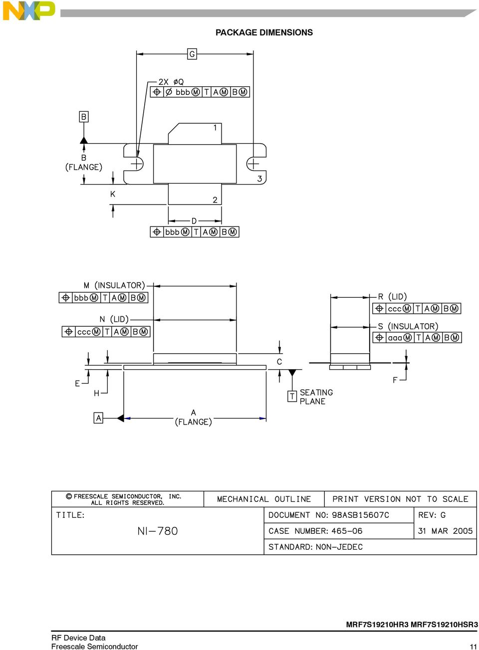
11 PACKAGE DIMENSIONS 11
12 12

13 13

14 14

15 PRODUCT DOCUMENTATION AND SOFTWARE Refer to the following documents and software to aid your design process. Application Notes AN1955: Thermal Measurement Methodology of RF Power Amplifiers Engineering Bulletins EB212: Using Data Sheet Impedances for RF LDMOS Devices Software Electromigration MTTF Calculator RF High Power Model For Software, do a Part Number search at and select the Part Number link. Go to the Software & Tools tab on the part s Product Summary page to download the respective tool. The following table summarizes revisions to this document. REVISION HISTORY Revision Date Description 0 Dec Initial Release of Data Sheet 1 Mar Modified data sheet to reflect RF Test Reduction described in Product and Process Change Notification number, PCN13628, p. 1, 2 Fig. 9, MTTF versus Junction Temperature removed, p. 7. Refer to the device s MTTF Calculator available at freescale.com/rfpower. Go to Design Resources > Software and Tools. Fig. 10, CCDF W--CDMA IQ Magnitude Clipping, Single--Carrier Test Signal and Fig. 11, Single--Carrier W--CDMA Spectrum updated to show the undistorted input test signal, p. 8 (renumbered as Figs. 9 and 10 respectively after Fig. 9 removed) Added Electromigration MTTF Calculator and RF High Power Model availability to Product Software, p

16 How to Reach Us: Home Page: Web Support: USA/Europe or Locations Not Listed:, Inc. Technical Information Center, EL East Elliot Road Tempe, Arizona or Europe, Middle East, and Africa: Freescale Halbleiter Deutschland GmbH Technical Information Center Schatzbogen Muenchen, Germany (English) (English) (German) (French) Japan: Japan Ltd. Headquarters ARCO Tower 15F , Shimo--Meguro, Meguro--ku, Tokyo Japan or [email protected] Asia/Pacific: China Ltd. Exchange Building 23F No. 118 Jianguo Road Chaoyang District Beijing China [email protected] For Literature Requests Only: Literature Distribution Center or Fax: [email protected] Information in this document is provided solely to enable system and software implementers to use products. There are no express or implied copyright licenses granted hereunder to design or fabricate any integrated circuits or integrated circuits based on the information in this document. reserves the right to make changes without further notice to any products herein. makes no warranty, representation or guarantee regarding the suitability of its products for any particular purpose, nor does assume any liability arising out of the application or use of any product or circuit, and specifically disclaims any and all liability, including without limitation consequential or incidental damages. Typical parameters that may be provided in data sheets and/or specifications can and do vary in different applications and actual performance may vary over time. All operating parameters, including Typicals, must be validated for each customer application by customer s technical experts. does not convey any license under its patent rights nor the rights of others. products are not designed, intended, or authorized for use as components in systems intended for surgical implant into the body, or other applications intended to support or sustain life, or for any other application in which the failure of the product could create a situation where personal injury or death may occur. Should Buyer purchase or use products for any such unintended or unauthorized application, Buyer shall indemnify and hold and its officers, employees, subsidiaries, affiliates, and distributors harmless against all claims, costs, damages, and expenses, and reasonable attorney fees arising out of, directly or indirectly, any claim of personal injury or death associated with such unintended or unauthorized use, even if such claim alleges that Freescale Semiconductor was negligent regarding the design or manufacture of the part. Freescalet and the Freescale logo are trademarks of, Inc. All other product or service names are the property of their respective owners., Inc. 2008, All rights reserved. Document Number: MRF7S19210H 16 Rev. 1, 3/2011
 +49 89 92103 559 (German) +33169354848(French) www.freescale.com/support Japan: Japan Ltd.")
RF Power LDMOS Transistors Enhancement--Mode Lateral MOSFETs
 Freescale Semiconductor Technical Data RF Power LDMOS Transistors Enhancement--Mode Lateral MOSFETs These 90 W RF power LDMOS transistors are designed for wideband RF power amplifiers covering the frequency
RF Power Field Effect Transistors N- Channel Enhancement- Mode Lateral MOSFETs
 Technical Data RF Power Field Effect Transistors N- Channel Enhancement- Mode Lateral MOSFETs Designed for GSM and GSM EDGE base station applications with frequencies from 864 to 894 MHz. Suitable for
NOT RECOMMENDED FOR NEW DESIGN
 Technical Data RF Power Field Effect Transistor N- Channel Enhancement- Mode Lateral MOSFET Designed for broadband commercial and industrial applications with frequencies up to 00 MHz. The high gain and
NOT RECOMMENDED FOR NEW DESIGN
 Technical Data RF Power Field Effect Transistor N-Channel Enhancement-Mode Lateral MOSFET Designed for broadband commercial and industrial applications with frequencies up to 00 MHz. The high gain and
NOT RECOMMENDED FOR NEW DESIGN
 Technical Data RF Power Field Effect Transistor N-Channel Enhancement-Mode Lateral MOSFET Designed for broadband commercial and industrial applications with frequencies up to 1000 MHz. The high gain and
RF Power Field Effect Transistors High Ruggedness N--Channel Enhancement--Mode Lateral MOSFETs
 Technical Data RF Power Field Effect Transistors High Ruggedness N--Channel Enhancement--Mode Lateral MOSFETs These high ruggedness devices are designed for use in high VSWR industrial (including laser
RF Power LDMOS Transistor High Ruggedness N--Channel Enhancement--Mode Lateral MOSFET
 Freescale Semiconductor Technical Data RF Power LDMOS Transistor High Ruggedness N--Channel Enhancement--Mode Lateral MOSFET RF power transistor suitable for both narrowband and broadband CW or pulse applications
UGF09030. 30W, 1 GHz, 26V Broadband RF Power N-Channel Enhancement-Mode Lateral MOSFET
 30W, 1 GHz, 26V Broadband RF Power N-Channel Enhancement-Mode Lateral MOSFET Designed for base station applications in the frequency band 800MHz to 1000MHz. Rated with a minimum output power of 30W, it
Connecting Low-Cost External Electrodes to MED-EKG
 Freescale Semiconductor Document Number: AN4223 Application Note Rev. 0, 11/2010 Connecting Low-Cost External Electrodes to MED-EKG by: Carlos Casillas RTAC Americas Guadalajara Mexico 1 Introduction This
Heterojunction Bipolar Transistor Technology (InGaP HBT) Broadband High Linearity Amplifier
 Broadband High Linearity Amplifier") Freescale Semiconductor Technical Data Heterojunction Bipolar Transistor Technology (InGaP HBT) Broadband High Linearity Amplifier The is a general purpose amplifier that is input and output internally
Freescale Semiconductor Technical Data Heterojunction Bipolar Transistor Technology (InGaP HBT) Broadband High Linearity Amplifier The is a general purpose amplifier that is input and output internally
IRTC Compensation and 1 Hz Clock Generation
 Freescale Semiconductor Document Number: AN4257 Application Note Rev. 0, January 2011 IRTC Compensation and 1 Hz Clock Generation by: Derek Liu Applications Engineering Shanghai 1 Introduction The MC9S08GW64
Freescale Semiconductor. Integrated Silicon Pressure Sensor. On-Chip Signal Conditioned, Temperature Compensated and Calibrated MPX4080D.
 Freescale Semiconductor Integrated Silicon Pressure Sensor + On-Chip Signal Conditioned, Temperature Compensated and Calibrated The series piezoresistive transducer is a state-of-the-art monolithic silicon
P D 215 1.25 Operating Junction Temperature T J 200 C Storage Temperature Range T stg 65 to +150 C
 SEMICONDUCTOR TECHNICAL DATA Order this document by /D The RF Line The is designed for output stages in band IV and V TV transmitter amplifiers. It incorporates high value emitter ballast resistors, gold
Windows 7: Using USB TAP on a Classic CodeWarrior Installation (MGT V9.2 DSC V8.3)
") Freescale Semiconductor Document Number: AN4338 Application Note Rev. 1.0, 12/2011 Windows 7: Using USB TAP on a Classic CodeWarrior Installation (MGT V9.2 DSC V8.3) Technical Information & Commercial
Freescale Semiconductor Document Number: AN4338 Application Note Rev. 1.0, 12/2011 Windows 7: Using USB TAP on a Classic CodeWarrior Installation (MGT V9.2 DSC V8.3) Technical Information & Commercial
MMBF4391LT1G, SMMBF4391LT1G, MMBF4392LT1G, MMBF4393LT1G. JFET Switching Transistors. N Channel
 LT1G, SLT1G, LT1G, LT1G JFET Switching Transistors NChannel Features S Prefix for Automotive and Other Applications Requiring Unique Site and Control Change Requirements; AECQ1 Qualified and PPAP Capable
How To Control A Motor Control On An Hvac Platform
 Freescale Semiconductor Document Number:AN4616 Application Note Rev. 0, 10/2012 Flap Motor Control Based On HVAC Platform by: Shawn Shi, Albert Chen, Alex Liu 1 Introduction According to the world market
NTMS4920NR2G. Power MOSFET 30 V, 17 A, N Channel, SO 8 Features
 NTMS9N Power MOSFET 3 V, 7 A, N Channel, SO Features Low R DS(on) to Minimize Conduction Losses Low Capacitance to Minimize Driver Losses Optimized Gate Charge to Minimize Switching Losses These Devices
MC13783 Buck and Boost Inductor Sizing
 Freescale Semiconductor Application Note Document Number: AN3294 Rev. 0.1, 01/2010 MC13783 Buck and Boost Inductor Sizing by: Power Management Application Team 1 Introduction The purpose of this application
Handling Freescale Pressure Sensors
 Freescale Semiconductor Application Note Rev 3, 11/2006 Handling Freescale Pressure by: William McDonald INTRODUCTION Smaller package outlines and higher board densities require the need for automated
2N5460, 2N5461, 2N5462. JFET Amplifier. P Channel Depletion. Pb Free Packages are Available* Features. http://onsemi.com MAXIMUM RATINGS
 2N546, 2N5461, JFET Amplifier PChannel Depletion Features PbFree Packages are Available* MAXIMUM RATINGS Rating Symbol Value Unit Drain Gate Voltage V DG 4 Vdc Reverse Gate Source Voltage V GSR 4 Vdc Forward
RF Power LDMOS Transistors High Ruggedness N--Channel Enhancement--Mode Lateral MOSFETs
 Freescale Semiconductor Technical Data RF Power LDMOS Transistors High Ruggedness N--Channel Enhancement--Mode Lateral MOSFETs RF power transistors designed for both narrowband and broadband ISM, broadcast
How To Build A Project On An Eclipse Powerbook For Anarc (Powerbook) On An Ipa (Powerpoint) On A Microcontroller (Powerboard) On Microcontrollers (Powerstation) On Your Microcontroller 2 (Powerclock
 On An Ipa (Powerpoint) On A Microcontroller (Powerboard) On Microcontrollers (Powerstation) On Your Microcontroller 2 (Powerclock") Freescale Semiconductor Document Number: AN4819 Application Note Rev. 1, 10/2013 Building a Project using IAR Eclipse Plugin Processor Expert Microcontrollers Driver Suite Processor Expert Microcontrollers
Freescale Semiconductor Document Number: AN4819 Application Note Rev. 1, 10/2013 Building a Project using IAR Eclipse Plugin Processor Expert Microcontrollers Driver Suite Processor Expert Microcontrollers
Connecting to an SMTP Server Using the Freescale NanoSSL Client
 Freescale Semiconductor Document Number: AN4363 Application Note Rev. 0, 10/2011 Connecting to an SMTP Server Using the Freescale NanoSSL Client by: Paolo Alcantara Microcontroller Solutions Group 1 Introduction
Hardware Configurations for the i.mx Family USB Modules
 Freescale Semiconductor Application Note Document Number: AN4136 Rev. 0, 06/2010 Hardware Configurations for the i.mx Family USB Modules by Multimedia Applications Division Freescale Semiconductor, Inc.
Local Interconnect Network (LIN) Physical Interface
 Physical Interface") Freescale Semiconductor Engineering Bulletin EB215 Rev. 1.0, 03/2005 Local Interconnect Network (LIN) Physical Interface Difference Between MC33399 and MC33661 Introduction This engineering bulletin highlights
Freescale Semiconductor Engineering Bulletin EB215 Rev. 1.0, 03/2005 Local Interconnect Network (LIN) Physical Interface Difference Between MC33399 and MC33661 Introduction This engineering bulletin highlights
Software Real Time Clock Implementation on MC9S08LG32
 Freescale Semiconductor Document Number: AN4478 Rev. 0, 03/2012 Software Real Time Clock Implementation on MC9S08LG32 by: Nitin Gupta Automotive and Industrial Solutions Group 1 Introduction The MC9S08LG32
Freescale Embedded GUI Converter Utility 2.0 Quick User Guide
 Freescale Semiconductor User Guide Document Number: EGUICUG Rev. 1, 08/2010 Freescale Embedded GUI Converter Utility 2.0 Quick User Guide 1 Introduction The Freescale Embedded GUI Converter Utility 2.0
Cyclic Redundant Checker Calculation on Power Architecture Technology and Comparison of Big-Endian Versus Little-Endian
 Freescale Semiconductor Document Number:AN4657 Application Note Rev. 0, 01/2013 Cyclic Redundant Checker Calculation on Power Architecture Technology and Comparison of Big-Endian Versus Little-Endian by:
Blood Pressure Monitor Using Flexis QE128 Gabriel Sanchez RTAC Americas
 Freescale Semiconductor Application Note Document Number: AN3500 Rev. 0, 08/2007 Blood Pressure Monitor Using Flexis QE128 by: Gabriel Sanchez RTAC Americas 1 Introduction Product designers and developers
Installation of the MMA955xL CodeWarrior Service Pack Author: Fengyi Li Application Engineer
 Freescale Semiconductor Application Note Document Number: AN4128 Rev. 0, 10/2011 Installation of the MMA955xL CodeWarrior Service Pack Author: Fengyi Li Application Engineer 1 Overview The Freescale MMA955xL
Flexible Active Shutter Control Interface using the MC1323x
 Freescale Semiconductor Document Number: AN4353 Application Note Rev. 0, 9/2011 Flexible Active Shutter Control Interface using the MC1323x by: Dennis Lui Freescale Hong Kong 1 Introduction This application
Using WinUSB in a Visual Studio Project with Freescale USB device controller
 Freescale Semiconductor Document Number: AN4378 Application Note Rev. 0, 10/2011 Using WinUSB in a Visual Studio Project with Freescale USB device controller by: Paolo Alcantara Microcontroller Solutions
Freescale Semiconductor. Integrated Silicon Pressure Sensor. On-Chip Signal Conditioned, Temperature Compensated and Calibrated MPX5500.
 Freescale Semiconductor Integrated Silicon Pressure Sensor + On-Chip Signal Conditioned, Temperature Compensated and Calibrated Series Pressure Rev 7, 09/2009 0 to 500 kpa (0 to 72.5 psi) 0.2 to 4.7 V
etpu Host Interface by:
 Freescale Semiconductor Application Note AN2821 Rev. 2, 08/2007 etpu Host Interface by: David Paterson Ming Li MCD Applications 1 Introduction This application note discusses the enhanced Time Processing
TSM2N7002K 60V N-Channel MOSFET
 SOT-23 SOT-323 Pin Definition: 1. Gate 2. Source 3. Drain PRODUCT SUMMARY V DS (V) R DS(on) (Ω) I D (ma) 5 @ V GS = 10V 100 60 5.5 @ V GS = 5V 100 Features Low On-Resistance ESD Protection High Speed Switching
BLL6G1214L-250. 1. Product profile. LDMOS L-band radar power transistor. 1.1 General description. 1.2 Features and benefits. 1.
 BLL6G1214L-25 Rev. 1 16 February 212 Preliminary data sheet 1. Product profile 1.1 General description 25 W LDMOS power transistor intended for L-band radar applications in the 1.2 GHz to 1.4 GHz range.
Simple Method of Changing the Frequency Range of a Power Amplifier Circuit
 Freescale Semiconductor Application Note AN4859 Rev. 0, 8/2014 Simple Method of Changing the Frequency Range of a Power Amplifier Circuit Amplifier designers often face the challenge of modifying an existing
Using the Performance Monitor Unit on the e200z760n3 Power Architecture Core
 Freescale Semiconductor Document Number: AN4341 Application Note Rev. 1, 08/2011 Using the Performance Monitor Unit on the e200z760n3 Power Architecture Core by: Inga Harris MSG Application Engineering
Features. Symbol JEDEC TO-220AB
 Data Sheet June 1999 File Number 2253.2 3A, 5V,.4 Ohm, N-Channel Power MOSFET This is an N-Channel enhancement mode silicon gate power field effect transistor designed for applications such as switching
PD 40 0.23 Storage Temperature Range Tstg 65 to +150 C Junction Temperature TJ 200 C
 SEMICONDUCTOR TECHNICAL DATA Order this document by MRF228/D The RF Line... designed for. volt VHF large signal power amplifiers in commercial and industrial FM equipment. Compact.28 Stud Package Specified.
How to Convert 3-Axis Directions and Swap X-Y Axis of Accelerometer Data within Android Driver by: Gang Chen Field Applications Engineer
 Freescale Semiconductor Application Note Document Number: AN4317 Rev. 0, 08/2011 How to Convert 3-Axis Directions and Swap X-Y Axis of Accelerometer Data within Android Driver by: Gang Chen Field Applications
2N6056. NPN Darlington Silicon Power Transistor DARLINGTON 8 AMPERE SILICON POWER TRANSISTOR 80 VOLTS, 100 WATTS
 NPN Darlington Silicon Power Transistor The NPN Darlington silicon power transistor is designed for general purpose amplifier and low frequency switching applications. High DC Current Gain h FE = 3000
Power MOSFET FEATURES. IRFZ44PbF SiHFZ44-E3 IRFZ44 SiHFZ44 T C = 25 C
 Power MOSFET PRODUCT SUMMARY (V) 60 R DS(on) (Ω) V GS = 10 V 0.028 Q g (Max.) (nc) 67 Q gs (nc) 18 Q gd (nc) 25 Configuration Single FEATURES Dynamic dv/dt Rating 175 C Operating Temperature Fast Switching
Power MOSFET FEATURES. IRL540PbF SiHL540-E3 IRL540 SiHL540
 Power MOSFET PRODUCT SUMMARY (V) 100 R DS(on) (Ω) = 5.0 V 0.077 Q g (Max.) (nc) 64 Q gs (nc) 9.4 Q gd (nc) 27 Configuration Single TO220AB G DS ORDERING INFORMATION Package Lead (Pb)free SnPb G D S NChannel
2N3906. General Purpose Transistors. PNP Silicon. Pb Free Packages are Available* http://onsemi.com. Features MAXIMUM RATINGS
 2N396 General Purpose Transistors PNP Silicon Features PbFree Packages are Available* COLLECTOR 3 MAXIMUM RATINGS Rating Symbol Value Unit Collector Emitter Voltage V CEO 4 Vdc Collector Base Voltage V
How To Measure Power Of A Permanent Magnet Synchronous Motor
 Freescale Semiconductor Document Number:AN4680 Application Note Rev. 0, 02/2013 PMSM Electrical Parameters Measurement by: Viktor Bobek 1 Introduction The vector control, also known as the field-oriented
Programming Audio Applications in the i.mx21 MC9328MX21
 Freescale Semiconductor Application Note Document Number: AN2628 Rev. 1, 10/2005 Programming Audio Applications in the MC9328MX21 by: Alfred Sin 1 Abstract The MC9328MX21 () processor has two dedicated
MPXAZ6115A MPXHZ6115A SERIES. Freescale Semiconductor Technical Data. MPXAZ6115A Rev 4, 01/2007
 Freescale Semiconductor Technical Data Media Resistant and High Temperature Accuracy Integrated Silicon Pressure Sensor for Measuring Absolute Pressure, On-Chip Signal Conditioned, Temperature Compensated
2N3903, 2N3904. General Purpose Transistors. NPN Silicon. Pb Free Packages are Available* Features. http://onsemi.com MAXIMUM RATINGS
 N393, General Purpose Transistors NPN Silicon Features PbFree Packages are Available* MAXIMUM RATINGS Rating Symbol Value Unit CollectorEmitter Voltage V CEO 4 Vdc CollectorBase Voltage V CBO 6 Vdc EmitterBase
Understanding LCD Memory and Bus Bandwidth Requirements ColdFire, LCD, and Crossbar Switch
 Freescale Semiconductor Application Note Document Number: AN3606 Rev. 0, 03/2008 Understanding LCD Memory and Bus Bandwidth Requirements ColdFire, LCD, and Crossbar Switch by: Melissa Hunter TSPG Applications
2N6387, 2N6388. Plastic Medium-Power Silicon Transistors DARLINGTON NPN SILICON POWER TRANSISTORS 8 AND 10 AMPERES 65 WATTS, 60-80 VOLTS
 2N6388 is a Preferred Device Plastic MediumPower Silicon Transistors These devices are designed for generalpurpose amplifier and lowspeed switching applications. Features High DC Current Gain h FE = 2500
Generate Makefiles from Command Line Support in Eclipse-Based CodeWarrior Software
 Freescale Semiconductor Document Number: AN4272 Application Note Rev. 0, 03/2011 Generate Makefiles from Command Line Support in Eclipse-Based CodeWarrior Software by Devtech Customer Engineering Freescale
Features. Description. Table 1. Device summary. Order code Marking Package Packing. STP110N8F6 110N8F6 TO-220 Tube
 N-channel 80 V, 0.0056 Ω typ.,110 A, STripFET F6 Power MOSFET in a TO-220 package Features Datasheet - production data Order code V DS R DS(on)max I D P TOT TAB STP110N8F6 80 V 0.0065 Ω 110 A 200 W TO-220
Power MOSFET FEATURES. IRF610PbF SiHF610-E3 IRF610 SiHF610. PARAMETER SYMBOL LIMIT UNIT Drain-Source Voltage V DS 200 V Gate-Source Voltage V GS ± 20
 Power MOSFET PRODUCT SUMMARY (V) 00 R DS(on) ( ) = 1.5 Q g (Max.) (nc) 8. Q gs (nc) 1.8 Q gd (nc) 4.5 Configuration Single FEATURES Dynamic dv/dt Rating Repetitive Avalanche Rated Fast Switching Ease of
Power MOSFET FEATURES. IRF740PbF SiHF740-E3 IRF740 SiHF740. PARAMETER SYMBOL LIMIT UNIT Drain-Source Voltage V DS 400 V Gate-Source Voltage V GS ± 20
 Power MOSFET PRODUCT SUMMARY (V) 400 R DS(on) (Ω) = 0.55 Q g (Max.) (nc) 63 Q gs (nc) 9.0 Q gd (nc) 3 Configuration Single FEATURES Dynamic dv/dt Rating Repetitive Avalanche Rated Fast Switching Ease of
ESD7484. 4-Line Ultra-Large Bandwidth ESD Protection
 4-Line Ultra-Large Bandwidth ESD Protection Functional Description The ESD7484 chip is a monolithic, application specific discrete device dedicated to ESD protection of the HDMI connection. It also offers
Ref Parameters Symbol Conditions Min Typ Max Units. Standby 3.5 10 μa. 3 Range 50 115 kpa. 4 Resolution 0.15 kpa. 5 Accuracy -20ºC to 85ºC ±1 kpa
 Freescale Semiconductor Miniature I 2 C Digital Barometer The is an absolute pressure sensor with digital output for low cost applications. A miniature 5 x 3 x 1.2 mm LGA package ideally suits it for portable
Improving Embedded Software Test Effectiveness in Automotive Applications
 Improving Embedded Software Test Effectiveness in Automotive Applications Author, D Brook Document Number: CODETESTTECHWP Rev. 0 11/2005 As the automotive industry introduces more and more safety-critical,
Initializing the TSEC Controller
 Freescale Semiconductor Application Note Document Number: AN2925 Rev. 0, 11/2005 Initializing the TSEC Controller by Ahsan Kabir Digital Systems Division Freescale Semiconductor, Inc. Austin, TX This application
Freescale Semiconductor. Integrated Silicon Pressure Sensor
 Freescale Semiconductor Rev 7, 1/2009 Integrated Silicon Sensor + Manifold Absolute Sensor On-Chip Signal Conditioned, Temperature Compensated and Calibrated The series Manifold Absolute (MAP) sensor for
2N3903, 2N3904. General Purpose Transistors. NPN Silicon. Features Pb Free Package May be Available. The G Suffix Denotes a Pb Free Lead Finish
 N393, N393 is a Preferred Device General Purpose Transistors NPN Silicon Features PbFree Package May be Available. The GSuffix Denotes a PbFree Lead Finish MAXIMUM RATINGS Rating Symbol Value Unit CollectorEmitter
STW20NM50 N-CHANNEL 550V @ Tjmax - 0.20Ω - 20ATO-247 MDmesh MOSFET
 N-CHANNEL 550V @ Tjmax - 0.20Ω - 20ATO-247 MDmesh MOSFET TYPE V DSS (@Tjmax) R DS(on) I D STW20NM50 550V < 0.25Ω 20 A TYPICAL R DS (on) = 0.20Ω HIGH dv/dt AND AVALANCHE CAPABILITIES 100% AVALANCHE TESTED
Power MOSFET. IRF510PbF SiHF510-E3 IRF510 SiHF510. PARAMETER SYMBOL LIMIT UNIT Drain-Source Voltage V DS 100 V Gate-Source Voltage V GS ± 20
 Power MOSFET PRODUCT SUMMARY (V) 100 R DS(on) () = 0.54 Q g max. (nc) 8.3 Q gs (nc) 2.3 Q gd (nc) 3.8 Configuration Single D TO220AB G FEATURES Dynamic dv/dt rating Available Repetitive avalanche rated
TQP0103 15 W, DC to 4 GHz, GaN Power Transistor
 Applications W-CDMA / LTE Macrocell Base Station Driver Microcell Base Station Small Cell Active Antenna General Purpose Applications 20 Pin 3x4mm QFN Product Features Functional Block Diagram Operating
Using eflexpwm Module for ADC Synchronization in MC56F82xx and MC56F84xx Family of Digital Signal Controllers
 Freescale Semiconductor Document Number:AN4675 Application Note Rev. 0, 01/2013 Using eflexpwm Module for ADC Synchronization in MC56F82xx and MC56F84xx Family of Digital Signal Controllers by: Pavel Grasblum
MCF54418 NAND Flash Controller
 Freescale Semiconductor Application Note Document Number: AN4348 Rev. 0, 09/2011 MCF54418 NAND Flash Controller by: Liew Tsi Chung Applications Engineer 1 Introduction The ColdFire MCF5441x family is the
MC33064DM 5 UNDERVOLTAGE SENSING CIRCUIT
 Order this document by MC3464/D The MC3464 is an undervoltage sensing circuit specifically designed for use as a reset controller in microprocessor-based systems. It offers the designer an economical solution
2N2222A. Small Signal Switching Transistor. NPN Silicon. MIL PRF 19500/255 Qualified Available as JAN, JANTX, and JANTXV. http://onsemi.com.
 Small Signal Switching Transistor NPN Silicon Features MILPRF19/ Qualified Available as JAN, JANTX, and JANTXV COLLECTOR MAXIMUM RATINGS (T A = unless otherwise noted) Characteristic Symbol Value Unit
STP80NF55-08 STB80NF55-08 STB80NF55-08-1 N-CHANNEL 55V - 0.0065 Ω - 80A D2PAK/I2PAK/TO-220 STripFET II POWER MOSFET
 STP80NF55-08 STB80NF55-08 STB80NF55-08-1 N-CHANNEL 55V - 0.0065 Ω - 80A D2PAK/I2PAK/TO-220 STripFET II POWER MOSFET TYPE V DSS R DS(on) I D STB80NF55-08/-1 STP80NF55-08 55 V 55 V
Vdc. Vdc. Adc. W W/ C T J, T stg 65 to + 200 C
 2N6284 (NPN); 2N6286, Preferred Device Darlington Complementary Silicon Power Transistors These packages are designed for general purpose amplifier and low frequency switching applications. Features High
STN3NF06L. N-channel 60 V, 0.07 Ω, 4 A, SOT-223 STripFET II Power MOSFET. Features. Application. Description
 N-channel 60 V, 0.07 Ω, 4 A, SOT-223 STripFET II Power MOSFET Features Type V DSS (@Tjmax) Exceptional dv/dt capability Avalanche rugged technology 100% avalanche tested R DS(on) max STN3NF06L 60 V < 0.1
MTD3055VT4. http://onsemi.com. MAXIMUM RATINGS (T C = 25 C unless otherwise noted) MARKING DIAGRAMS ORDERING INFORMATION. R DS(on) TYP 60 V 100 m
 MARKING DIAGRAMS ORDERING INFORMATION. R DS(on) TYP 60 V 100 m") MTD55V Preferred Device Power MOSFET Amps, 6 Volts NChannel This Power MOSFET is designed to withstand high energy in the avalanche and commutation modes. Designed for low voltage, high speed switching
MTD55V Preferred Device Power MOSFET Amps, 6 Volts NChannel This Power MOSFET is designed to withstand high energy in the avalanche and commutation modes. Designed for low voltage, high speed switching
STP60NF06. N-channel 60V - 0.014Ω - 60A TO-220 STripFET II Power MOSFET. General features. Description. Internal schematic diagram.
 N-channel 60V - 0.014Ω - 60A TO-220 STripFET II Power MOSFET General features Type V DSS R DS(on) I D STP60NF06 60V
BUZ11. 30A, 50V, 0.040 Ohm, N-Channel Power MOSFET. Features. [ /Title (BUZ1 1) /Subject. (30A, 50V, 0.040 Ohm, N- Channel. Ordering Information
 /Subject. (30A, 50V, 0.040 Ohm, N- Channel. Ordering Information") Data Sheet June 1999 File Number 2253.2 [ /Title (BUZ1 1) /Subject (3A, 5V,.4 Ohm, N- Channel Power MOS- FET) /Autho r () /Keywords (Intersil Corporation, N- Channel Power MOS- FET, TO- 22AB ) /Creator
Data Sheet June 1999 File Number 2253.2 [ /Title (BUZ1 1) /Subject (3A, 5V,.4 Ohm, N- Channel Power MOS- FET) /Autho r () /Keywords (Intersil Corporation, N- Channel Power MOS- FET, TO- 22AB ) /Creator
P2N2222ARL1G. Amplifier Transistors. NPN Silicon. These are Pb Free Devices* Features. http://onsemi.com
 Amplifier Transistors NPN Silicon Features These are PbFree Devices* MAXIMUM RATINGS (T A = 25 C unless otherwise noted) Characteristic Symbol Value Unit CollectorEmitter Voltage V CEO 4 CollectorBase
Pressure Freescale Semiconductor
 Freescale Semiconductor Integrated Silicon Sensor On-Chip Signal Conditioned, Temperature Compensated and Calibrated The series piezoresistive transducer is a state-of-the-art monolithic silicon pressure
2N4401. General Purpose Transistors. NPN Silicon. Pb Free Packages are Available* http://onsemi.com. Features MAXIMUM RATINGS THERMAL CHARACTERISTICS
 General Purpose Transistors NPN Silicon Features PbFree Packages are Available* MAXIMUM RATINGS Rating Symbol Value Unit Collector Emitter Voltage V CEO 4 Vdc Collector Base Voltage V CBO 6 Vdc Emitter
Power MOSFET FEATURES. IRF740PbF SiHF740-E3 IRF740 SiHF740. PARAMETER SYMBOL LIMIT UNIT Drain-Source Voltage V DS 400 V Gate-Source Voltage V GS ± 20
 Power MOSFET PRODUCT SUMMARY (V) 400 R DS(on) (Ω) = 0.55 Q g (Max.) (nc) 63 Q gs (nc) 9.0 Q gd (nc) 3 Configuration Single FEATURES Dynamic dv/dt Rating Repetitive Avalanche Rated Fast Switching Ease of
N-Channel 20-V (D-S) 175 C MOSFET
 175 C MOSFET") N-Channel -V (D-S) 75 C MOSFET SUD7N-4P PRODUCT SUMMARY V DS (V) r DS(on) ( ) (A) a.37 @ V GS = V 37.6 @ V GS = 4.5 V 9 TO-5 D FEATURES TrenchFET Power MOSFET 75 C Junction Temperature PWM Optimized for
N-Channel -V (D-S) 75 C MOSFET SUD7N-4P PRODUCT SUMMARY V DS (V) r DS(on) ( ) (A) a.37 @ V GS = V 37.6 @ V GS = 4.5 V 9 TO-5 D FEATURES TrenchFET Power MOSFET 75 C Junction Temperature PWM Optimized for
STP60NF06FP. N-channel 60V - 0.014Ω - 30A TO-220FP STripFET II Power MOSFET. General features. Description. Internal schematic diagram.
 N-channel 60V - 0.014Ω - 30A TO-220FP STripFET II Power MOSFET General features Type V DSS R DS(on) I D STP60NF06FP 60V
LOW POWER NARROWBAND FM IF
 Order this document by MC336B/D The MC336B includes an Oscillator, Mixer, Limiting Amplifier, Quadrature Discriminator, Active Filter, Squelch, Scan Control and Mute Switch. This device is designed for
TIP41, TIP41A, TIP41B, TIP41C (NPN); TIP42, TIP42A, TIP42B, TIP42C (PNP) Complementary Silicon Plastic Power Transistors
; TIP42, TIP42A, TIP42B, TIP42C (PNP) Complementary Silicon Plastic Power Transistors") TIP41, TIP41A, TIP41B, TIP41C (NPN); TIP42, TIP42A, TIP42B, TIP42C (PNP) Complementary Silicon Plastic Power Transistors Designed for use in general purpose amplifier and switching applications. Features
TIP41, TIP41A, TIP41B, TIP41C (NPN); TIP42, TIP42A, TIP42B, TIP42C (PNP) Complementary Silicon Plastic Power Transistors Designed for use in general purpose amplifier and switching applications. Features
MC10SX1190. Fibre Channel Coaxial Cable Driver and Loop Resiliency Circuit
 Fibre Channel Coaxial Cable Driver and Loop Resiliency Circuit Description The MC10SX1190 is a differential receiver, differential transmitter specifically designed to drive coaxial cables. It incorporates
Point-of-Sale (POS) Users Guide Lech José Olmedo Guerrero Jaime Herrerro Gallardo RTAC Americas
 Users Guide Lech José Olmedo Guerrero Jaime Herrerro Gallardo RTAC Americas") Freescale Semiconductor Users Guide Document Number: POSUG Rev. 0, 03/2007 Point-of-Sale (POS) Users Guide by: Lech José Olmedo Guerrero Jaime Herrerro Gallardo RTAC Americas 1 Introduction This quick
Freescale Semiconductor Users Guide Document Number: POSUG Rev. 0, 03/2007 Point-of-Sale (POS) Users Guide by: Lech José Olmedo Guerrero Jaime Herrerro Gallardo RTAC Americas 1 Introduction This quick
MPS2222, MPS2222A. NPN Silicon. Pb Free Packages are Available* http://onsemi.com. Features MAXIMUM RATINGS MARKING DIAGRAMS THERMAL CHARACTERISTICS
 , is a Preferred Device General Purpose Transistors NPN Silicon Features PbFree Packages are Available* COLLECTOR 3 MAXIMUM RATINGS CollectorEmitter Voltage CollectorBase Voltage Rating Symbol Value Unit
N-Channel 60-V (D-S), 175 C MOSFET
, 175 C MOSFET") N-Channel 6-V (D-S), 75 C MOSFET SUP/SUB7N6-4 V (BR)DSS (V) r DS(on) ( ) (A) 6.4 7 a TO-22AB D TO-263 DRAIN connected to TAB G G D S Top View SUP7N6-4 G D S Top View SUB7N6-4 S N-Channel MOSFET Parameter
N-Channel 6-V (D-S), 75 C MOSFET SUP/SUB7N6-4 V (BR)DSS (V) r DS(on) ( ) (A) 6.4 7 a TO-22AB D TO-263 DRAIN connected to TAB G G D S Top View SUP7N6-4 G D S Top View SUB7N6-4 S N-Channel MOSFET Parameter
IRF740 N-CHANNEL 400V - 0.46Ω - 10A TO-220 PowerMESH II MOSFET
 N-CHANNEL 400V - 0.46Ω - 10A TO-220 PowerMESH II MOSFET TYPE V DSS R DS(on) I D IRF740 400 V < 0.55 Ω 10 A TYPICAL R DS (on) = 0.46Ω EXCEPTIONAL dv/dt CAPABILITY 100% AVALANCHE TESTED LOW GATE CHARGE VERY
Power MOSFET FEATURES. IRF520PbF SiHF520-E3 IRF520 SiHF520. PARAMETER SYMBOL LIMIT UNIT Drain-Source Voltage V DS 100 V Gate-Source Voltage V GS ± 20
 Power MOSFET PRODUCT SUMMARY (V) 100 R DS(on) ( ) = 0.7 Q g (Max.) (nc) 16 Q gs (nc) 4.4 Q gd (nc) 7.7 Configuration Single TO0AB G DS ORDERING INFORMATION Package Lead (Pb)free SnPb G D S NChannel MOSFET
TPN4R712MD TPN4R712MD. 1. Applications. 2. Features. 3. Packaging and Internal Circuit. 2014-12 2015-04-21 Rev.4.0. Silicon P-Channel MOS (U-MOS )
") MOSFETs Silicon P-Channel MOS (U-MOS) TPN4R712MD TPN4R712MD 1. Applications Lithium-Ion Secondary Batteries Power Management Switches 2. Features (1) Low drain-source on-resistance: R DS(ON) = 3.8 mω (typ.)
MOSFETs Silicon P-Channel MOS (U-MOS) TPN4R712MD TPN4R712MD 1. Applications Lithium-Ion Secondary Batteries Power Management Switches 2. Features (1) Low drain-source on-resistance: R DS(ON) = 3.8 mω (typ.)
How To Fit A 2Mm Exposed Pad To A Dfn Package
 EVERSPIN s New 2mm Exposed Pad DFN Package Meets Both SOIC-8 and DFN8 PCB Layouts This Application Note is to inform Everspin customers that a new, DFN8 package with a 2mm bottom exposed pad has been added
PowerQUICC II Pro (MPC83xx) PCI Agent Initialization
 PCI Agent Initialization") Freescale Semiconductor Application Note Document Number: AN3373 Rev. 0, 04/2007 PowerQUICC II Pro (MPC83xx) PCI Agent Initialization by: David Smith Field Application Engineering Raleigh, NC In many designs,
Freescale Semiconductor Application Note Document Number: AN3373 Rev. 0, 04/2007 PowerQUICC II Pro (MPC83xx) PCI Agent Initialization by: David Smith Field Application Engineering Raleigh, NC In many designs,
OptiMOS Power-Transistor Product Summary
 OptiMOS Power-Transistor Product Summary V DS 55 V R DS(on),max 4) 35 mω Features Dual N-channel Logic Level - Enhancement mode AEC Q11 qualified I D 2 A PG-TDSON-8-4 MSL1 up to 26 C peak reflow 175 C
BC546B, BC547A, B, C, BC548B, C. Amplifier Transistors. NPN Silicon. Pb Free Package is Available* Features. http://onsemi.com MAXIMUM RATINGS
 B, A, B, C, B, C Amplifier Transistors NPN Silicon Features PbFree Package is Available* COLLECTOR 1 2 BASE MAXIMUM RATINGS Collector-Emitter oltage Collector-Base oltage Rating Symbol alue Unit CEO 65
Symbol Parameters Units Frequency Min. Typ. Max. 850 MHz 14.8 16.3 17.8
 Product Description Sirenza Microdevices SGC-689Z is a high performance SiGe HBT MMIC amplifier utilizing a Darlington configuration with a patented active-bias network. The active bias network provides
MITSUBISHI RF MOSFET MODULE RA07H4047M
 MITSUBISHI RF MOSFET MODULE RA7H7M RoHS Compliance,-7MHz 7W.V, Stage Amp. For PORTABLE RADIO DESCRIPTION The RA7H7M is a 7-watt RF MOSFET Amplifier Module for.-volt portable radios that operate in the
Performance Monitor on PowerQUICC II Pro Processors
 Freescale Semiconductor Application Note Document Number: AN3359 Rev. 0, 05/2007 Performance Monitor on PowerQUICC II Pro Processors by Harinder Rai Network Computing Systems Group Freescale Semiconductor,
P-Channel 1.25-W, 1.8-V (G-S) MOSFET
 MOSFET") Si5DS P-Channel.5-W,.-V (G-S) MOSFET PRODUCT SUMMARY V DS (V) R DS(on) (Ω) I D (A).5 at V GS = -.5 V ±.5 -.7 at V GS = -.5 V ±. at V GS = -. V ± FEATURES Halogen-free According to IEC 9-- Available TrenchFET
Si5DS P-Channel.5-W,.-V (G-S) MOSFET PRODUCT SUMMARY V DS (V) R DS(on) (Ω) I D (A).5 at V GS = -.5 V ±.5 -.7 at V GS = -.5 V ±. at V GS = -. V ± FEATURES Halogen-free According to IEC 9-- Available TrenchFET
DISCRETE SEMICONDUCTORS DATA SHEET M3D060. BLF177 HF/VHF power MOS transistor. Product specification Supersedes data of 1998 Jul 02.
 DISCRETE SEMICONDUCTORS DATA SHEET M3D6 Supersedes data of 1998 Jul 2 23 Jul 21 FEATURES High power gain Low intermodulation distortion Easy power control Good thermal stability Withstands full load mismatch.
BC327, BC327-16, BC327-25, BC327-40. Amplifier Transistors. PNP Silicon. These are Pb Free Devices* http://onsemi.com. Features MAXIMUM RATINGS
 BC327, BC327-16, BC327-25, BC327-4 Amplifier Transistors PNP Silicon Features These are PbFree Devices* MAXIMUM RATINGS Rating Symbol Value Unit CollectorEmitter Voltage V CEO 45 Vdc CollectorEmitter Voltage