RF Power Field Effect Transistors High Ruggedness N--Channel Enhancement--Mode Lateral MOSFETs
|
|
|
- Dwayne Benjamin Martin
- 9 years ago
- Views:
Transcription
1 Technical Data RF Power Field Effect Transistors High Ruggedness N--Channel Enhancement--Mode Lateral MOSFETs These high ruggedness devices are designed for use in high VSWR industrial (including laser and plasma exciters), broadcast (analog and digital), aerospace and radio/land mobile applications. They are unmatched input and output designs allowing wide frequency range utilization, between 1.8 and 600 MHz. Typical Performance: V DD =50Volts,I DQ = 100 ma Signal Type Pulsed (100 μsec, 20% Duty Cycle) P out (W) f (MHz) G ps (db) η D (%) IRL (db) 300 Peak CW 300 Avg Capable of Handling a Load Mismatch of 65:1 50 Vdc, 230 MHz, at all Phase Angles 300 Watts CW Output Power 300 Watts Pulsed Peak Power, 20% Duty Cycle, 100 μsec Capable of 300 Watts CW Operation Features Unmatched Input and Output Allowing Wide Frequency Range Utilization Device can be used Single--Ended or in a Push--Pull Configuration Qualified Up to a Maximum of 50 V DD Operation Characterized from 30 V to 50 V for Extended Power Range Suitable for Linear Application with Appropriate Biasing Integrated ESD Protection Greater Negative Gate--Source Voltage Range for Improved Class C Operation Characterized with Series Equivalent Large--Signal Impedance Parameters RoHS Compliant NI in Tape and Reel. R3 Suffix = 250 Units, 56 mm Tape Width, 13 inch Reel. For R5 Tape and Reel options, see p. 14. NI--780S--4 in Tape and Reel. R3 Suffix = 250 Units, 32 mm Tape Width, 13 inch Reel. For R5 Tape and Reel options, see p. 14. Table 1. Maximum Ratings Rating Symbol Value Unit Drain--Source Voltage V DSS --0.5, +130 Vdc Gate--Source Voltage V GS --6.0, +10 Vdc Storage Temperature Range T stg --65 to +150 C Case Operating Temperature T C 150 C Total Device T C =25 C Derate above 25 C P D W W/ C Operating Junction Temperature (1,2) T J 225 C Table 2. Thermal Characteristics Characteristic Symbol Value (2,3) Unit C/W Thermal Resistance, Junction to Case (4) Pulsed: Case Temperature 75 C, 300 W Pulsed, 100 μsec Pulse Width, 20% Duty Cycle, 50 Vdc, I DQ = 100 ma, 230 MHz CW: Case Temperature 87 C, 300 W CW, 50 Vdc, I DQ = 1100 ma, 230 MHz Document Number: MRFE6VP6300H Rev. 1, 7/2011 MRFE6VP6300HR3 MRFE6VP6300HSR MHz, 300 W, 50 V LATERAL N -CHANNEL BROADBAND RF POWER MOSFETs CASE 465M -01, STYLE 1 NI MRFE6VP6300HR3 CASE 465H -02, STYLE 1 NI -780S -4 MRFE6VP6300HSR3 RF in /V GS RF in /V GS 3 1 (Top View) Z θjc 0.05 R θjc Continuous use at maximum temperature will affect MTTF. 2. MTTF calculator available at Select Software & Tools/Development Tools/Calculators to access MTTF calculators by product. 3. Refer to AN1955, Thermal Measurement Methodology of RF Power Amplifiers. Go to Select Documentation/Application Notes -- AN Same test circuit is used for both pulsed and CW. RF out /V DS 4 2 RF out /V DS Figure 1. Pin Connections, Inc., All rights reserved. 1
 P out (W) f (MHz) G ps (db) η D (%) IRL (db) 300 Peak 230 26.5 74.0 -- 16 CW 300 Avg. 130 25.0 80.")
2 Table 3. ESD Protection Characteristics Test Methodology Human Body Model (per JESD22--A114) Machine Model (per EIA/JESD22--A115) Charge Device Model (per JESD22--C101) Class 2 (Minimum) B (Minimum) IV (Minimum) Table 4. Electrical Characteristics (T A =25 C unless otherwise noted) Characteristic Symbol Min Typ Max Unit Off Characteristics (1) Gate--Source Leakage Current (V GS =5Vdc,V DS =0Vdc) I GSS 1 μadc Drain--Source Breakdown Voltage (V GS =0Vdc,I D =50mA) Zero Gate Voltage Drain Leakage Current (V DS =50Vdc,V GS =0Vdc) Zero Gate Voltage Drain Leakage Current (V DS = 100 Vdc, V GS =0Vdc) On Characteristics Gate Threshold Voltage (1) (V DS =10Vdc,I D = 480 μadc) Gate Quiescent Voltage (V DD =50Vdc,I D = 100 madc, Measured in Functional Test) Drain--Source On--Voltage (1) (V GS =10Vdc,I D =1Adc) Dynamic Characteristics (1) Reverse Transfer Capacitance (V DS =50Vdc± 30 1 MHz, V GS =0Vdc) Output Capacitance (V DS =50Vdc± 30 1 MHz, V GS =0Vdc) Input Capacitance (V DS =50Vdc,V GS =0Vdc± 30 1 MHz) V (BR)DSS 130 Vdc I DSS 5 μadc I DSS 10 μadc V GS(th) Vdc V GS(Q) Vdc V DS(on) 0.25 Vdc C rss 0.8 pf C oss 76 pf C iss 188 pf Functional Tests (In Freescale Test Fixture, 50 ohm system) V DD =50Vdc,I DQ = 100 ma, P out = 300 W Peak (60 W Avg.), f = 230 MHz, Pulsed, 100 μsec Pulse Width, 20% Duty Cycle Power Gain G ps db Drain Efficiency η D % Input Return Loss IRL db Load Mismatch (In Freescale Application Test Fixture, 50 ohm system) V DD =50Vdc,I DQ = 100 ma VSWR 65:1 at all Phase Angles Pulsed: P out = 300 W Peak (60 W Avg.), f = 230 MHz, Pulsed, 100 μsec Pulse Width, 20% Duty Cycle CW: P out = 300 W Avg., f = 130 MHz Ψ No Degradation in Output Power 1. Each side of device measured separately. 2
 Characteristic Symbol Min Typ Max Unit Off Characteristics (1) Gate--Source Leakage Current (V GS =5Vdc,V DS =0Vdc) I GSS 1 μadc")
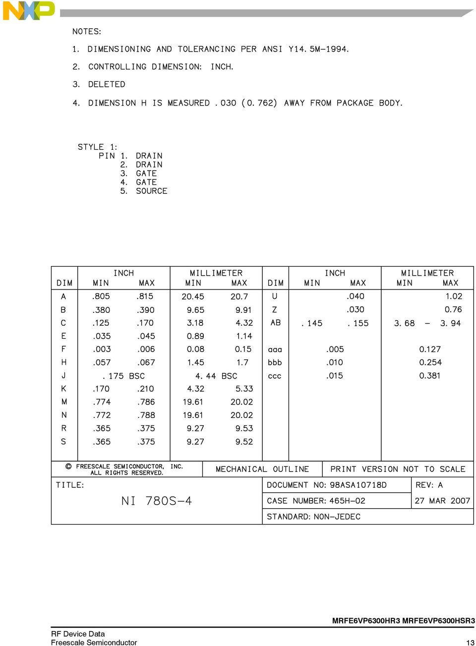
3 V BIAS + C8 L1 C9 + C14 + C15 C10 C11 C12 C13 + C16 V SUPPLY RF INPUT Z1 C1 C4 Z2 C5 C2 Z3 C6 C7 Z4 Z5 C3 R1 Z6 Z7 DUT Z8 Z9 L2 Z10 C17 Z11 C18 C19 Z12 C20 Z13 RF OUTPUT Z x Microstrip Z2* x Microstrip Z3* x Microstrip Z x Microstrip Z x Microstrip Z x Microstrip Z7, Z x Microstrip Z x Microstrip Z10* x Microstrip Z11* x Microstrip Z12* x Microstrip Z x Microstrip * Line length includes microstrip bends Note: Same test circuit is used for both pulsed and CW. Figure 2. MRFE6VP6300HR3(HSR3) Test Circuit Schematic Table 5. MRFE6VP6300HR3(HSR3) Test Circuit Component Designations and Values Part Description Part Number Manufacturer C1, C20 15 pf Chip Capacitors ATC100B150JT500XT ATC C2 82 pf Chip Capacitor ATC100B820JT500XT ATC C3, C17 91 pf Chip Capacitors ATC100B910JT500XT ATC C4, C pf Chip Capacitors ATC100B102JT50XT ATC C5, C11 10K pf Chip Capacitors ATC200B103KT50XT ATC C6 0.1 μf, 50 V Chip Capacitor CDR33BX104AKWS AVX C7 2.2 μf, 100 V Chip Capacitor HMK432B7225KM--T Taiyo Yuden C8 10 μf, 35 V Tantalum Capacitor T491D106K035AT Kemet C9 2.2 μf, 100 V Chip Capacitor G2225X7R225KT3AB ATC C μf, 100 V Chip Capacitor C1812F104K1RAC Kemet C μf, 100 V Chip Capacitor C1825C103K1GAC Kemet C14, C15, C μf, 100 V Electolytic Capacitors MCGPR100V227M16X26--RH Multicomp C18, C19 18 pf Chip Capacitors ATC100B180JT500XT ATC L1 120 nh Inductor 1812SMS--R12JLC Coilcraft L nh Inductor GA3095--ALC Coilcraft R Ω, 1/2 W Chip Resistor CRCW20101K00FKEF Vishay PCB 0.030, ε r =2.55 AD255A Arlon 3
 Test Circuit Schematic Table 5.")
4 C8 C14 C15 L1 C13 C16 C6 C5 C7 C9 C10 C12 C11 C1 C4 C3 R1 L2 C17 C18 C20 C2 CUT OUT AREA C19 MRFE6VP6300H/HS Rev. 2 Figure 3. MRFE6VP6300HR3(HSR3) Test Circuit Component Layout 4
 Test Circuit Component")
5 TYPICAL CHARACTERISTICS PULSED C, CAPACITANCE (pf) Measured with ±30 1 MHz 54 V GS =0Vdc V DS, DRAIN--SOURCE VOLTAGE (VOLTS) Note: Each side of device measured separately. Figure 4. Capacitance versus Drain -Source Voltage C iss C oss C rss P out, OUTPUT POWER (dbm) PULSED P1dB = 55.4 dbm (344 W) P3dB = 56.0 dbm (398 W) P2dB = 55.8 dbm (380 W) Ideal Actual V DD =50Vdc,I DQ = 100 ma, f = 230 MHz Pulse Width = 100 μsec, 20% Duty Cycle P in, INPUT POWER (dbm) PULSED Figure 5. Pulsed Output Power versus Input Power 34 G ps, POWER GAIN (db) V DD =50Vdc,I DQ = 100 ma, f = 230 MHz Pulse Width = 100 μsec, 20% Duty Cycle G ps 23 η D P out, OUTPUT POWER (WATTS) PULSED η D, DRAIN EFFICIENCY (%) G ps, POWER GAIN (db) V DD =50Vdc,I DQ = 100 ma, f = 230 MHz Pulse Width = 100 μsec, 20% Duty Cycle 50 V DD =30V 35 V 40 V P out, OUTPUT POWER (WATTS) PULSED 45 V 50 V Figure 6. Pulsed Power Gain and Drain Efficiency versus Output Power Figure 7. Pulsed Power Gain versus Output Power η D, DRAIN EFFICIENCY (%) V DD =30V 35 V 40 V 45 V V DD =50Vdc,I DQ = 100 ma, f = 230 MHz Pulse Width = 100 μsec, 20% Duty Cycle V 400 G ps, POWER GAIN (db) V DD =50Vdc,I DQ = 100 ma, f = 230 MHz Pulse Width = 100 μsec, 20% Duty Cycle T C =--30_C 85_C η D 25_C G ps 85_C 25_C --30_C η D, DRAIN EFFICIENCY (%) P out, OUTPUT POWER (WATTS) PULSED P out, OUTPUT POWER (WATTS) PULSED Figure 8. Pulsed Drain Efficiency versus Output Power Figure 9. Pulsed Power Gain and Drain Efficiency versus Output Power 5
 Ideal Actual V DD =50Vdc,I DQ = 100 ma, f = 230 MHz Pulse Width = 100 μsec, 20% Duty Cycle 27 28 29 30 31 32 33 P in, INPUT POWER (dbm) PULSED Figure 5.")
6 TYPICAL CHARACTERISTICS TWO -TONE (1) IMD, INTERMODULATION DISTORTION (dbc) V DD =50Vdc,I DQ = 1600 ma, f1 = 230 MHz f2 = MHz, Two--Tone Measurements 3rd Order 5th Order 7th Order IMD, INTERMODULATION DISTORTION (dbc) V DD =50Vdc,P out = 250 W (PEP)/62.5 W Avg. per Tone I DQ = 1600 ma, Two--Tone Measurements 3rd Order 5th Order 7th Order P out, OUTPUT POWER (WATTS) PEP TWO--TONE SPACING (MHz) Figure 10. Intermodulation Distortion Products versus Output Power Figure 11. Intermodulation Distortion Products versus Two -Tone Spacing G ps, POWER GAIN (db) I DQ = 1600 ma 1400 ma 1100 ma 900 ma 650 ma V DD = 50 Vdc, f1 = 230 MHz, f2 = MHz Two--Tone Measurements IMD, THIRD ORDER INTERMODULATION DISTORTION (dbc) V DD = 50 Vdc, f1 = 230 MHz, f2 = MHz Two--Tone Measurements I DQ = 650 ma 900 ma 1400 ma 1100 ma 1600 ma P out, OUTPUT POWER (WATTS) PEP Figure 12. Two -Tone Power Gain versus Output Power P out, OUTPUT POWER (WATTS) PEP Figure 13. Third Order Intermodulation Distortion versus Output Power 1. The distortion products are referenced to one of the two tones and the peak envelope power (PEP) is 6 db above the power in a single tone. 6

7 TYPICAL CHARACTERISTICS V DD =50Vdc P out = 300 W Avg. η D = 80% MTTF (HOURS) T J, JUNCTION TEMPERATURE ( C) MTTF calculator available at Select Software & Tools/Development Tools/Calculators to access MTTF calculators by product. Figure 14. MTTF versus Junction Temperature CW 250 7

8 Z source f = 230 MHz Z load f = 230 MHz Z o =5Ω f MHz V DD =50Vdc,I DQ = 100 ma, P out = 300 W Peak Z source Ω Z load Ω j j2.85 Z source = Test circuit impedance as measured from gate to ground. Z load = Test circuit impedance as measured from drain to ground. Input Matching Network Device Under Test Output Matching Network Z source Z load Figure 15. Series Equivalent Source and Load Impedance 8

9 f MHz V DD =50Vdc,I DQ = 100 ma Z source Ω Z load Ω j j j j j j j j j j j j j j j j j j Simulated performance at 1 db gain compression. Z source = Source impedance presented from gate to gate. Z load = Load impedance presented from drain to drain. Source + Device Under Test -- Load -- + Z source Z load Figure 16. Simulated Source and Load Impedances Optimized for IRL, Output Power and Drain Efficiency Push -Pull 9

10 PACKAGE DIMENSIONS 10

11 11

12 12
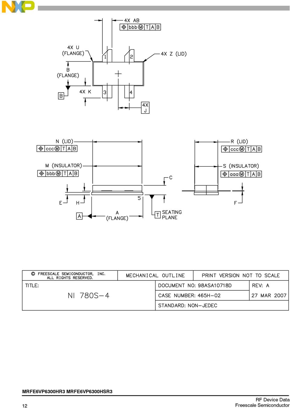
13 13
14 PRODUCT DOCUMENTATION AND SOFTWARE Refer to the following documents to aid your design process. Application Notes AN1955: Thermal Measurement Methodology of RF Power Amplifiers Engineering Bulletins EB212: Using Data Sheet Impedances for RF LDMOS Devices Software Electromigration MTTF Calculator RF High Power Model.s2p File For Software, do a Part Number search at and select the Part Number link. Go to the Software & Tools tab on the part s Product Summary page to download the respective tool. R5 TAPE AND REEL OPTION NI = R5 Suffix = 50 Units, 56 mm Tape Width, 13 inch Reel. NI--780S--4 = R5 Suffix = 50 Units, 32 mm Tape Width, 13 inch Reel. The R5 tape and reel option for MRFE6VP6300H and MRFE6VP6300HS parts will be available for 2 years after release of MRFE6VP6300H and MRFE6VP6300HS., Inc. reserves the right to limit the quantities that will be delivered in the R5 tape and reel option. At the end of the 2 year period customers who have purchased these devices in the R5 tape and reel option will be offered MRFE6VP6300H and MRFE6VP6300HS in the R3 tape and reel option. The following table summarizes revisions to this document. REVISION HISTORY Revision Date Description 0 Oct Initial Release of Data Sheet 1 July 2011 Corrected pin 4 label from RF out /V GS to RF in /V GS, Fig. 1, Pin Connections, p. 1 Changed Drain--Source voltage from --0.5, +125 to --0.5, +130 in Maximum Ratings table, p. 1 Added Total Device Dissipation to Maximum Ratings table, p. 1 Changed V (BR)DSS Min value from 125 to 130 Vdc, Table 4, Off Characteristics, p. 2 Tightened V GS(th) Min limit from 1.5 to 1.7 Vdc and Max limit from 3.0 to 2.7 Vdc as a result of process improvement, Table 4, On Characteristics, p. 2 Tightened V GS(Q) Min limit from 1.7 to 2.0 Vdc and Max limit from 3.2 to 3.0 Vdc as a result of process improvement, Table 4, On Characteristics, p. 2 Added Load Mismatch table to Table 4. Electrical Characteristics, p. 2 MTTF end temperature on graph changed to match maximum operating junction temperature, Fig. 14, MTTF versus Junction Temperature, p. 7 Added Fig. 16, Simulated Source and Load Impedances Optimized for IRL, Output Power and Drain Efficiency Push--Pull table, p. 9 14

15 How to Reach Us: Home Page: Web Support: USA/Europe or Locations Not Listed:, Inc. Technical Information Center, EL East Elliot Road Tempe, Arizona or Europe, Middle East, and Africa: Freescale Halbleiter Deutschland GmbH Technical Information Center Schatzbogen Muenchen, Germany (English) (English) (German) (French) Japan: Japan Ltd. Headquarters ARCO Tower 15F , Shimo--Meguro, Meguro--ku, Tokyo Japan or [email protected] Asia/Pacific: China Ltd. Exchange Building 23F No. 118 Jianguo Road Chaoyang District Beijing China [email protected] For Literature Requests Only: Literature Distribution Center or Fax: [email protected] Information in this document is provided solely to enable system and software implementers to use products. There are no express or implied copyright licenses granted hereunder to design or fabricate any integrated circuits or integrated circuits based on the information in this document. reserves the right to make changes without further notice to any products herein. makes no warranty, representation or guarantee regarding the suitability of its products for any particular purpose, nor does assume any liability arising out of the application or use of any product or circuit, and specifically disclaims any and all liability, including without limitation consequential or incidental damages. Typical parameters that may be provided in data sheets and/or specifications can and do vary in different applications and actual performance may vary over time. All operating parameters, including Typicals, must be validated for each customer application by customer s technical experts. does not convey any license under its patent rights nor the rights of others. products are not designed, intended, or authorized for use as components in systems intended for surgical implant into the body, or other applications intended to support or sustain life, or for any other application in which the failure of the product could create a situation where personal injury or death may occur. Should Buyer purchase or use products for any such unintended or unauthorized application, Buyer shall indemnify and hold and its officers, employees, subsidiaries, affiliates, and distributors harmless against all claims, costs, damages, and expenses, and reasonable attorney fees arising out of, directly or indirectly, any claim of personal injury or death associated with such unintended or unauthorized use, even if such claim alleges that Freescale Semiconductor was negligent regarding the design or manufacture of the part. Freescalet and the Freescale logo are trademarks of, Inc. All other product or service names are the property of their respective owners., Inc All rights reserved. RF Document DeviceNumber: Data MRFE6VP6300H Freescale Rev. 1, 7/2011 Semiconductor 15
 +49 89 92103 559 (German) +33169354848(French) www.freescale.com/support Japan: Japan Ltd.")
RF Power LDMOS Transistor High Ruggedness N--Channel Enhancement--Mode Lateral MOSFET
 Freescale Semiconductor Technical Data RF Power LDMOS Transistor High Ruggedness N--Channel Enhancement--Mode Lateral MOSFET RF power transistor suitable for both narrowband and broadband CW or pulse applications
NOT RECOMMENDED FOR NEW DESIGN
 Technical Data RF Power Field Effect Transistor N- Channel Enhancement- Mode Lateral MOSFET Designed for broadband commercial and industrial applications with frequencies up to 00 MHz. The high gain and
NOT RECOMMENDED FOR NEW DESIGN
 Technical Data RF Power Field Effect Transistor N-Channel Enhancement-Mode Lateral MOSFET Designed for broadband commercial and industrial applications with frequencies up to 00 MHz. The high gain and
RF Power Field Effect Transistors N- Channel Enhancement- Mode Lateral MOSFETs
 Technical Data RF Power Field Effect Transistors N- Channel Enhancement- Mode Lateral MOSFETs Designed for GSM and GSM EDGE base station applications with frequencies from 864 to 894 MHz. Suitable for
RF Power LDMOS Transistors Enhancement--Mode Lateral MOSFETs
 Freescale Semiconductor Technical Data RF Power LDMOS Transistors Enhancement--Mode Lateral MOSFETs These 90 W RF power LDMOS transistors are designed for wideband RF power amplifiers covering the frequency
NOT RECOMMENDED FOR NEW DESIGN
 Technical Data RF Power Field Effect Transistor N-Channel Enhancement-Mode Lateral MOSFET Designed for broadband commercial and industrial applications with frequencies up to 1000 MHz. The high gain and
RF Power Field Effect Transistors N--Channel Enhancement--Mode Lateral MOSFETs
 Technical Data RF Power Field Effect Transistors N--Channel Enhancement--Mode Lateral MOSFETs Designed for CDMA base station applications with frequencies from 1930 to 1990 MHz. Can be used in Class AB
RF Power LDMOS Transistors High Ruggedness N--Channel Enhancement--Mode Lateral MOSFETs
 Freescale Semiconductor Technical Data RF Power LDMOS Transistors High Ruggedness N--Channel Enhancement--Mode Lateral MOSFETs RF power transistors designed for both narrowband and broadband ISM, broadcast
UGF09030. 30W, 1 GHz, 26V Broadband RF Power N-Channel Enhancement-Mode Lateral MOSFET
 30W, 1 GHz, 26V Broadband RF Power N-Channel Enhancement-Mode Lateral MOSFET Designed for base station applications in the frequency band 800MHz to 1000MHz. Rated with a minimum output power of 30W, it
Heterojunction Bipolar Transistor Technology (InGaP HBT) Broadband High Linearity Amplifier
 Broadband High Linearity Amplifier") Freescale Semiconductor Technical Data Heterojunction Bipolar Transistor Technology (InGaP HBT) Broadband High Linearity Amplifier The is a general purpose amplifier that is input and output internally
Freescale Semiconductor Technical Data Heterojunction Bipolar Transistor Technology (InGaP HBT) Broadband High Linearity Amplifier The is a general purpose amplifier that is input and output internally
2N5460, 2N5461, 2N5462. JFET Amplifier. P Channel Depletion. Pb Free Packages are Available* Features. http://onsemi.com MAXIMUM RATINGS
 2N546, 2N5461, JFET Amplifier PChannel Depletion Features PbFree Packages are Available* MAXIMUM RATINGS Rating Symbol Value Unit Drain Gate Voltage V DG 4 Vdc Reverse Gate Source Voltage V GSR 4 Vdc Forward
MMBF4391LT1G, SMMBF4391LT1G, MMBF4392LT1G, MMBF4393LT1G. JFET Switching Transistors. N Channel
 LT1G, SLT1G, LT1G, LT1G JFET Switching Transistors NChannel Features S Prefix for Automotive and Other Applications Requiring Unique Site and Control Change Requirements; AECQ1 Qualified and PPAP Capable
MC13783 Buck and Boost Inductor Sizing
 Freescale Semiconductor Application Note Document Number: AN3294 Rev. 0.1, 01/2010 MC13783 Buck and Boost Inductor Sizing by: Power Management Application Team 1 Introduction The purpose of this application
Connecting Low-Cost External Electrodes to MED-EKG
 Freescale Semiconductor Document Number: AN4223 Application Note Rev. 0, 11/2010 Connecting Low-Cost External Electrodes to MED-EKG by: Carlos Casillas RTAC Americas Guadalajara Mexico 1 Introduction This
NTMS4920NR2G. Power MOSFET 30 V, 17 A, N Channel, SO 8 Features
 NTMS9N Power MOSFET 3 V, 7 A, N Channel, SO Features Low R DS(on) to Minimize Conduction Losses Low Capacitance to Minimize Driver Losses Optimized Gate Charge to Minimize Switching Losses These Devices
Freescale Semiconductor. Integrated Silicon Pressure Sensor. On-Chip Signal Conditioned, Temperature Compensated and Calibrated MPX4080D.
 Freescale Semiconductor Integrated Silicon Pressure Sensor + On-Chip Signal Conditioned, Temperature Compensated and Calibrated The series piezoresistive transducer is a state-of-the-art monolithic silicon
IRTC Compensation and 1 Hz Clock Generation
 Freescale Semiconductor Document Number: AN4257 Application Note Rev. 0, January 2011 IRTC Compensation and 1 Hz Clock Generation by: Derek Liu Applications Engineering Shanghai 1 Introduction The MC9S08GW64
P D 215 1.25 Operating Junction Temperature T J 200 C Storage Temperature Range T stg 65 to +150 C
 SEMICONDUCTOR TECHNICAL DATA Order this document by /D The RF Line The is designed for output stages in band IV and V TV transmitter amplifiers. It incorporates high value emitter ballast resistors, gold
How To Build A Project On An Eclipse Powerbook For Anarc (Powerbook) On An Ipa (Powerpoint) On A Microcontroller (Powerboard) On Microcontrollers (Powerstation) On Your Microcontroller 2 (Powerclock
 On An Ipa (Powerpoint) On A Microcontroller (Powerboard) On Microcontrollers (Powerstation) On Your Microcontroller 2 (Powerclock") Freescale Semiconductor Document Number: AN4819 Application Note Rev. 1, 10/2013 Building a Project using IAR Eclipse Plugin Processor Expert Microcontrollers Driver Suite Processor Expert Microcontrollers
Freescale Semiconductor Document Number: AN4819 Application Note Rev. 1, 10/2013 Building a Project using IAR Eclipse Plugin Processor Expert Microcontrollers Driver Suite Processor Expert Microcontrollers
Windows 7: Using USB TAP on a Classic CodeWarrior Installation (MGT V9.2 DSC V8.3)
") Freescale Semiconductor Document Number: AN4338 Application Note Rev. 1.0, 12/2011 Windows 7: Using USB TAP on a Classic CodeWarrior Installation (MGT V9.2 DSC V8.3) Technical Information & Commercial
Freescale Semiconductor Document Number: AN4338 Application Note Rev. 1.0, 12/2011 Windows 7: Using USB TAP on a Classic CodeWarrior Installation (MGT V9.2 DSC V8.3) Technical Information & Commercial
Flexible Active Shutter Control Interface using the MC1323x
 Freescale Semiconductor Document Number: AN4353 Application Note Rev. 0, 9/2011 Flexible Active Shutter Control Interface using the MC1323x by: Dennis Lui Freescale Hong Kong 1 Introduction This application
Freescale Embedded GUI Converter Utility 2.0 Quick User Guide
 Freescale Semiconductor User Guide Document Number: EGUICUG Rev. 1, 08/2010 Freescale Embedded GUI Converter Utility 2.0 Quick User Guide 1 Introduction The Freescale Embedded GUI Converter Utility 2.0
Installation of the MMA955xL CodeWarrior Service Pack Author: Fengyi Li Application Engineer
 Freescale Semiconductor Application Note Document Number: AN4128 Rev. 0, 10/2011 Installation of the MMA955xL CodeWarrior Service Pack Author: Fengyi Li Application Engineer 1 Overview The Freescale MMA955xL
Cyclic Redundant Checker Calculation on Power Architecture Technology and Comparison of Big-Endian Versus Little-Endian
 Freescale Semiconductor Document Number:AN4657 Application Note Rev. 0, 01/2013 Cyclic Redundant Checker Calculation on Power Architecture Technology and Comparison of Big-Endian Versus Little-Endian by:
Handling Freescale Pressure Sensors
 Freescale Semiconductor Application Note Rev 3, 11/2006 Handling Freescale Pressure by: William McDonald INTRODUCTION Smaller package outlines and higher board densities require the need for automated
PD 40 0.23 Storage Temperature Range Tstg 65 to +150 C Junction Temperature TJ 200 C
 SEMICONDUCTOR TECHNICAL DATA Order this document by MRF228/D The RF Line... designed for. volt VHF large signal power amplifiers in commercial and industrial FM equipment. Compact.28 Stud Package Specified.
How To Control A Motor Control On An Hvac Platform
 Freescale Semiconductor Document Number:AN4616 Application Note Rev. 0, 10/2012 Flap Motor Control Based On HVAC Platform by: Shawn Shi, Albert Chen, Alex Liu 1 Introduction According to the world market
2N6056. NPN Darlington Silicon Power Transistor DARLINGTON 8 AMPERE SILICON POWER TRANSISTOR 80 VOLTS, 100 WATTS
 NPN Darlington Silicon Power Transistor The NPN Darlington silicon power transistor is designed for general purpose amplifier and low frequency switching applications. High DC Current Gain h FE = 3000
BLL6G1214L-250. 1. Product profile. LDMOS L-band radar power transistor. 1.1 General description. 1.2 Features and benefits. 1.
 BLL6G1214L-25 Rev. 1 16 February 212 Preliminary data sheet 1. Product profile 1.1 General description 25 W LDMOS power transistor intended for L-band radar applications in the 1.2 GHz to 1.4 GHz range.
Hardware Configurations for the i.mx Family USB Modules
 Freescale Semiconductor Application Note Document Number: AN4136 Rev. 0, 06/2010 Hardware Configurations for the i.mx Family USB Modules by Multimedia Applications Division Freescale Semiconductor, Inc.
Local Interconnect Network (LIN) Physical Interface
 Physical Interface") Freescale Semiconductor Engineering Bulletin EB215 Rev. 1.0, 03/2005 Local Interconnect Network (LIN) Physical Interface Difference Between MC33399 and MC33661 Introduction This engineering bulletin highlights
Freescale Semiconductor Engineering Bulletin EB215 Rev. 1.0, 03/2005 Local Interconnect Network (LIN) Physical Interface Difference Between MC33399 and MC33661 Introduction This engineering bulletin highlights
TSM2N7002K 60V N-Channel MOSFET
 SOT-23 SOT-323 Pin Definition: 1. Gate 2. Source 3. Drain PRODUCT SUMMARY V DS (V) R DS(on) (Ω) I D (ma) 5 @ V GS = 10V 100 60 5.5 @ V GS = 5V 100 Features Low On-Resistance ESD Protection High Speed Switching
Connecting to an SMTP Server Using the Freescale NanoSSL Client
 Freescale Semiconductor Document Number: AN4363 Application Note Rev. 0, 10/2011 Connecting to an SMTP Server Using the Freescale NanoSSL Client by: Paolo Alcantara Microcontroller Solutions Group 1 Introduction
Software Real Time Clock Implementation on MC9S08LG32
 Freescale Semiconductor Document Number: AN4478 Rev. 0, 03/2012 Software Real Time Clock Implementation on MC9S08LG32 by: Nitin Gupta Automotive and Industrial Solutions Group 1 Introduction The MC9S08LG32
Simple Method of Changing the Frequency Range of a Power Amplifier Circuit
 Freescale Semiconductor Application Note AN4859 Rev. 0, 8/2014 Simple Method of Changing the Frequency Range of a Power Amplifier Circuit Amplifier designers often face the challenge of modifying an existing
Freescale Semiconductor. Integrated Silicon Pressure Sensor. On-Chip Signal Conditioned, Temperature Compensated and Calibrated MPX5500.
 Freescale Semiconductor Integrated Silicon Pressure Sensor + On-Chip Signal Conditioned, Temperature Compensated and Calibrated Series Pressure Rev 7, 09/2009 0 to 500 kpa (0 to 72.5 psi) 0.2 to 4.7 V
MPXAZ6115A MPXHZ6115A SERIES. Freescale Semiconductor Technical Data. MPXAZ6115A Rev 4, 01/2007
 Freescale Semiconductor Technical Data Media Resistant and High Temperature Accuracy Integrated Silicon Pressure Sensor for Measuring Absolute Pressure, On-Chip Signal Conditioned, Temperature Compensated
Power MOSFET FEATURES. IRFZ44PbF SiHFZ44-E3 IRFZ44 SiHFZ44 T C = 25 C
 Power MOSFET PRODUCT SUMMARY (V) 60 R DS(on) (Ω) V GS = 10 V 0.028 Q g (Max.) (nc) 67 Q gs (nc) 18 Q gd (nc) 25 Configuration Single FEATURES Dynamic dv/dt Rating 175 C Operating Temperature Fast Switching
Power MOSFET FEATURES. IRL540PbF SiHL540-E3 IRL540 SiHL540
 Power MOSFET PRODUCT SUMMARY (V) 100 R DS(on) (Ω) = 5.0 V 0.077 Q g (Max.) (nc) 64 Q gs (nc) 9.4 Q gd (nc) 27 Configuration Single TO220AB G DS ORDERING INFORMATION Package Lead (Pb)free SnPb G D S NChannel
2N3903, 2N3904. General Purpose Transistors. NPN Silicon. Features Pb Free Package May be Available. The G Suffix Denotes a Pb Free Lead Finish
 N393, N393 is a Preferred Device General Purpose Transistors NPN Silicon Features PbFree Package May be Available. The GSuffix Denotes a PbFree Lead Finish MAXIMUM RATINGS Rating Symbol Value Unit CollectorEmitter
Using WinUSB in a Visual Studio Project with Freescale USB device controller
 Freescale Semiconductor Document Number: AN4378 Application Note Rev. 0, 10/2011 Using WinUSB in a Visual Studio Project with Freescale USB device controller by: Paolo Alcantara Microcontroller Solutions
Generate Makefiles from Command Line Support in Eclipse-Based CodeWarrior Software
 Freescale Semiconductor Document Number: AN4272 Application Note Rev. 0, 03/2011 Generate Makefiles from Command Line Support in Eclipse-Based CodeWarrior Software by Devtech Customer Engineering Freescale
etpu Host Interface by:
 Freescale Semiconductor Application Note AN2821 Rev. 2, 08/2007 etpu Host Interface by: David Paterson Ming Li MCD Applications 1 Introduction This application note discusses the enhanced Time Processing
Vdc. Vdc. Adc. W W/ C T J, T stg 65 to + 200 C
 2N6284 (NPN); 2N6286, Preferred Device Darlington Complementary Silicon Power Transistors These packages are designed for general purpose amplifier and low frequency switching applications. Features High
DISCRETE SEMICONDUCTORS DATA SHEET. BLF244 VHF power MOS transistor
 DISCRETE SEMICONDUCTORS DATA SHEET September 1992 FEATURES High power gain Low noise figure Easy power control Good thermal stability Withstands full load mismatch Gold metallization ensures excellent
Blood Pressure Monitor Using Flexis QE128 Gabriel Sanchez RTAC Americas
 Freescale Semiconductor Application Note Document Number: AN3500 Rev. 0, 08/2007 Blood Pressure Monitor Using Flexis QE128 by: Gabriel Sanchez RTAC Americas 1 Introduction Product designers and developers
Freescale Semiconductor. Integrated Silicon Pressure Sensor
 Freescale Semiconductor Rev 7, 1/2009 Integrated Silicon Sensor + Manifold Absolute Sensor On-Chip Signal Conditioned, Temperature Compensated and Calibrated The series Manifold Absolute (MAP) sensor for
1SMB59xxBT3G Series, SZ1SMB59xxT3G Series. 3 Watt Plastic Surface Mount Zener Voltage Regulators
 9xxBTG Series, SZ9xxTG Series Watt Plastic Surface Mount Zener Voltage Regulators This complete new line of W Zener diodes offers the following advantages. Features Zener Voltage Range. V to V ESD Rating
Power MOSFET FEATURES. IRF610PbF SiHF610-E3 IRF610 SiHF610. PARAMETER SYMBOL LIMIT UNIT Drain-Source Voltage V DS 200 V Gate-Source Voltage V GS ± 20
 Power MOSFET PRODUCT SUMMARY (V) 00 R DS(on) ( ) = 1.5 Q g (Max.) (nc) 8. Q gs (nc) 1.8 Q gd (nc) 4.5 Configuration Single FEATURES Dynamic dv/dt Rating Repetitive Avalanche Rated Fast Switching Ease of
STN3NF06L. N-channel 60 V, 0.07 Ω, 4 A, SOT-223 STripFET II Power MOSFET. Features. Application. Description
 N-channel 60 V, 0.07 Ω, 4 A, SOT-223 STripFET II Power MOSFET Features Type V DSS (@Tjmax) Exceptional dv/dt capability Avalanche rugged technology 100% avalanche tested R DS(on) max STN3NF06L 60 V < 0.1
Power MOSFET. IRF510PbF SiHF510-E3 IRF510 SiHF510. PARAMETER SYMBOL LIMIT UNIT Drain-Source Voltage V DS 100 V Gate-Source Voltage V GS ± 20
 Power MOSFET PRODUCT SUMMARY (V) 100 R DS(on) () = 0.54 Q g max. (nc) 8.3 Q gs (nc) 2.3 Q gd (nc) 3.8 Configuration Single D TO220AB G FEATURES Dynamic dv/dt rating Available Repetitive avalanche rated
2N4401. General Purpose Transistors. NPN Silicon. Pb Free Packages are Available* http://onsemi.com. Features MAXIMUM RATINGS THERMAL CHARACTERISTICS
 General Purpose Transistors NPN Silicon Features PbFree Packages are Available* MAXIMUM RATINGS Rating Symbol Value Unit Collector Emitter Voltage V CEO 4 Vdc Collector Base Voltage V CBO 6 Vdc Emitter
MMBZ52xxBLT1G Series, SZMMBZ52xxBLT3G. Zener Voltage Regulators. 225 mw SOT 23 Surface Mount
 MMBZ5xxBLTG Series, SZMMBZ5xxBLTG Series Zener Voltage Regulators 5 mw SOT Surface Mount This series of Zener diodes is offered in the convenient, surface mount plastic SOT package. These devices are designed
BC327, BC327-16, BC327-25, BC327-40. Amplifier Transistors. PNP Silicon. These are Pb Free Devices* http://onsemi.com. Features MAXIMUM RATINGS
 BC327, BC327-16, BC327-25, BC327-4 Amplifier Transistors PNP Silicon Features These are PbFree Devices* MAXIMUM RATINGS Rating Symbol Value Unit CollectorEmitter Voltage V CEO 45 Vdc CollectorEmitter Voltage
Using eflexpwm Module for ADC Synchronization in MC56F82xx and MC56F84xx Family of Digital Signal Controllers
 Freescale Semiconductor Document Number:AN4675 Application Note Rev. 0, 01/2013 Using eflexpwm Module for ADC Synchronization in MC56F82xx and MC56F84xx Family of Digital Signal Controllers by: Pavel Grasblum
P2N2222ARL1G. Amplifier Transistors. NPN Silicon. These are Pb Free Devices* Features. http://onsemi.com
 Amplifier Transistors NPN Silicon Features These are PbFree Devices* MAXIMUM RATINGS (T A = 25 C unless otherwise noted) Characteristic Symbol Value Unit CollectorEmitter Voltage V CEO 4 CollectorBase
How to Convert 3-Axis Directions and Swap X-Y Axis of Accelerometer Data within Android Driver by: Gang Chen Field Applications Engineer
 Freescale Semiconductor Application Note Document Number: AN4317 Rev. 0, 08/2011 How to Convert 3-Axis Directions and Swap X-Y Axis of Accelerometer Data within Android Driver by: Gang Chen Field Applications
Power MOSFET FEATURES. IRF740PbF SiHF740-E3 IRF740 SiHF740. PARAMETER SYMBOL LIMIT UNIT Drain-Source Voltage V DS 400 V Gate-Source Voltage V GS ± 20
 Power MOSFET PRODUCT SUMMARY (V) 400 R DS(on) (Ω) = 0.55 Q g (Max.) (nc) 63 Q gs (nc) 9.0 Q gd (nc) 3 Configuration Single FEATURES Dynamic dv/dt Rating Repetitive Avalanche Rated Fast Switching Ease of
Features. Symbol JEDEC TO-220AB
 Data Sheet June 1999 File Number 2253.2 3A, 5V,.4 Ohm, N-Channel Power MOSFET This is an N-Channel enhancement mode silicon gate power field effect transistor designed for applications such as switching
MCR08B, MCR08M. Sensitive Gate Silicon Controlled Rectifiers. Reverse Blocking Thyristors. SCRs 0.8 AMPERES RMS 200 thru 600 VOLTS
 MCR8B, MCR8M Sensitive Gate Silicon Controlled Rectifiers Reverse Blocking Thyristors PNPN devices designed for line powered consumer applications such as relay and lamp drivers, small motor controls,
TIP41, TIP41A, TIP41B, TIP41C (NPN); TIP42, TIP42A, TIP42B, TIP42C (PNP) Complementary Silicon Plastic Power Transistors
; TIP42, TIP42A, TIP42B, TIP42C (PNP) Complementary Silicon Plastic Power Transistors") TIP41, TIP41A, TIP41B, TIP41C (NPN); TIP42, TIP42A, TIP42B, TIP42C (PNP) Complementary Silicon Plastic Power Transistors Designed for use in general purpose amplifier and switching applications. Features
TIP41, TIP41A, TIP41B, TIP41C (NPN); TIP42, TIP42A, TIP42B, TIP42C (PNP) Complementary Silicon Plastic Power Transistors Designed for use in general purpose amplifier and switching applications. Features
STP60NF06. N-channel 60V - 0.014Ω - 60A TO-220 STripFET II Power MOSFET. General features. Description. Internal schematic diagram.
 N-channel 60V - 0.014Ω - 60A TO-220 STripFET II Power MOSFET General features Type V DSS R DS(on) I D STP60NF06 60V
STP80NF55-08 STB80NF55-08 STB80NF55-08-1 N-CHANNEL 55V - 0.0065 Ω - 80A D2PAK/I2PAK/TO-220 STripFET II POWER MOSFET
 STP80NF55-08 STB80NF55-08 STB80NF55-08-1 N-CHANNEL 55V - 0.0065 Ω - 80A D2PAK/I2PAK/TO-220 STripFET II POWER MOSFET TYPE V DSS R DS(on) I D STB80NF55-08/-1 STP80NF55-08 55 V 55 V
2N6387, 2N6388. Plastic Medium-Power Silicon Transistors DARLINGTON NPN SILICON POWER TRANSISTORS 8 AND 10 AMPERES 65 WATTS, 60-80 VOLTS
 2N6388 is a Preferred Device Plastic MediumPower Silicon Transistors These devices are designed for generalpurpose amplifier and lowspeed switching applications. Features High DC Current Gain h FE = 2500
MC14008B. 4-Bit Full Adder
 4-Bit Full Adder The MC4008B 4bit full adder is constructed with MOS PChannel and NChannel enhancement mode devices in a single monolithic structure. This device consists of four full adders with fast
2N2222A. Small Signal Switching Transistor. NPN Silicon. MIL PRF 19500/255 Qualified Available as JAN, JANTX, and JANTXV. http://onsemi.com.
 Small Signal Switching Transistor NPN Silicon Features MILPRF19/ Qualified Available as JAN, JANTX, and JANTXV COLLECTOR MAXIMUM RATINGS (T A = unless otherwise noted) Characteristic Symbol Value Unit
STW20NM50 N-CHANNEL 550V @ Tjmax - 0.20Ω - 20ATO-247 MDmesh MOSFET
 N-CHANNEL 550V @ Tjmax - 0.20Ω - 20ATO-247 MDmesh MOSFET TYPE V DSS (@Tjmax) R DS(on) I D STW20NM50 550V < 0.25Ω 20 A TYPICAL R DS (on) = 0.20Ω HIGH dv/dt AND AVALANCHE CAPABILITIES 100% AVALANCHE TESTED
TPN4R712MD TPN4R712MD. 1. Applications. 2. Features. 3. Packaging and Internal Circuit. 2014-12 2015-04-21 Rev.4.0. Silicon P-Channel MOS (U-MOS )
") MOSFETs Silicon P-Channel MOS (U-MOS) TPN4R712MD TPN4R712MD 1. Applications Lithium-Ion Secondary Batteries Power Management Switches 2. Features (1) Low drain-source on-resistance: R DS(ON) = 3.8 mω (typ.)
MOSFETs Silicon P-Channel MOS (U-MOS) TPN4R712MD TPN4R712MD 1. Applications Lithium-Ion Secondary Batteries Power Management Switches 2. Features (1) Low drain-source on-resistance: R DS(ON) = 3.8 mω (typ.)
MPS2222, MPS2222A. NPN Silicon. Pb Free Packages are Available* http://onsemi.com. Features MAXIMUM RATINGS MARKING DIAGRAMS THERMAL CHARACTERISTICS
 , is a Preferred Device General Purpose Transistors NPN Silicon Features PbFree Packages are Available* COLLECTOR 3 MAXIMUM RATINGS CollectorEmitter Voltage CollectorBase Voltage Rating Symbol Value Unit
DISCRETE SEMICONDUCTORS DATA SHEET M3D060. BLF177 HF/VHF power MOS transistor. Product specification Supersedes data of 1998 Jul 02.
 DISCRETE SEMICONDUCTORS DATA SHEET M3D6 Supersedes data of 1998 Jul 2 23 Jul 21 FEATURES High power gain Low intermodulation distortion Easy power control Good thermal stability Withstands full load mismatch.
MMSZxxxT1G Series, SZMMSZxxxT1G Series. Zener Voltage Regulators. 500 mw SOD 123 Surface Mount
 MMSZxxxTG Series, SZMMSZxxxTG Series Zener Voltage Regulators 5 mw SOD 3 Surface Mount Three complete series of Zener diodes are offered in the convenient, surface mount plastic SOD 3 package. These devices
SSM3K335R SSM3K335R. 1. Applications. 2. Features. 3. Packaging and Pin Configuration. 2012-07-19 Rev.3.0. Silicon N-Channel MOS (U-MOS -H)
") MOSFETs Silicon N-Channel MOS (U-MOS-H) SSM3K335R SSM3K335R 1. Applications Power Management Switches DC-DC Converters 2. Features (1) 4.5-V gate drive voltage. (2) Low drain-source on-resistance : R DS(ON)
MOSFETs Silicon N-Channel MOS (U-MOS-H) SSM3K335R SSM3K335R 1. Applications Power Management Switches DC-DC Converters 2. Features (1) 4.5-V gate drive voltage. (2) Low drain-source on-resistance : R DS(ON)
Using the Performance Monitor Unit on the e200z760n3 Power Architecture Core
 Freescale Semiconductor Document Number: AN4341 Application Note Rev. 1, 08/2011 Using the Performance Monitor Unit on the e200z760n3 Power Architecture Core by: Inga Harris MSG Application Engineering
LM350. 3.0 A, Adjustable Output, Positive Voltage Regulator THREE TERMINAL ADJUSTABLE POSITIVE VOLTAGE REGULATOR
 3. A, able Output, Positive Voltage Regulator The is an adjustable threeterminal positive voltage regulator capable of supplying in excess of 3. A over an output voltage range of 1.2 V to 33 V. This voltage
P-Channel 1.25-W, 1.8-V (G-S) MOSFET
 MOSFET") Si5DS P-Channel.5-W,.-V (G-S) MOSFET PRODUCT SUMMARY V DS (V) R DS(on) (Ω) I D (A).5 at V GS = -.5 V ±.5 -.7 at V GS = -.5 V ±. at V GS = -. V ± FEATURES Halogen-free According to IEC 9-- Available TrenchFET
Si5DS P-Channel.5-W,.-V (G-S) MOSFET PRODUCT SUMMARY V DS (V) R DS(on) (Ω) I D (A).5 at V GS = -.5 V ±.5 -.7 at V GS = -.5 V ±. at V GS = -. V ± FEATURES Halogen-free According to IEC 9-- Available TrenchFET
1N59xxBRNG Series. 3 W DO-41 Surmetic 30 Zener Voltage Regulators
 W DO-4 Surmetic 0 Zener Voltage Regulators This is a N9xxBRNG series with limits and excellent operating characteristics that reflect the superior capabilities of silicon oxide passivated junctions. All
BC546B, BC547A, B, C, BC548B, C. Amplifier Transistors. NPN Silicon. Pb Free Package is Available* Features. http://onsemi.com MAXIMUM RATINGS
 B, A, B, C, B, C Amplifier Transistors NPN Silicon Features PbFree Package is Available* COLLECTOR 1 2 BASE MAXIMUM RATINGS Collector-Emitter oltage Collector-Base oltage Rating Symbol alue Unit CEO 65
MTD3055VT4. http://onsemi.com. MAXIMUM RATINGS (T C = 25 C unless otherwise noted) MARKING DIAGRAMS ORDERING INFORMATION. R DS(on) TYP 60 V 100 m
 MARKING DIAGRAMS ORDERING INFORMATION. R DS(on) TYP 60 V 100 m") MTD55V Preferred Device Power MOSFET Amps, 6 Volts NChannel This Power MOSFET is designed to withstand high energy in the avalanche and commutation modes. Designed for low voltage, high speed switching
MTD55V Preferred Device Power MOSFET Amps, 6 Volts NChannel This Power MOSFET is designed to withstand high energy in the avalanche and commutation modes. Designed for low voltage, high speed switching
Features. Description. Table 1. Device summary. Order code Marking Package Packing. STP110N8F6 110N8F6 TO-220 Tube
 N-channel 80 V, 0.0056 Ω typ.,110 A, STripFET F6 Power MOSFET in a TO-220 package Features Datasheet - production data Order code V DS R DS(on)max I D P TOT TAB STP110N8F6 80 V 0.0065 Ω 110 A 200 W TO-220
Programming Audio Applications in the i.mx21 MC9328MX21
 Freescale Semiconductor Application Note Document Number: AN2628 Rev. 1, 10/2005 Programming Audio Applications in the MC9328MX21 by: Alfred Sin 1 Abstract The MC9328MX21 () processor has two dedicated
STP62NS04Z N-CHANNEL CLAMPED 12.5mΩ - 62A TO-220 FULLY PROTECTED MESH OVERLAY MOSFET
 N-CHANNEL CLAMPED 12.5mΩ - 62A TO-220 FULLY PROTECTED MESH OVERLAY MOSFET TYPE V DSS R DS(on) I D STP62NS04Z CLAMPED
2N3906. General Purpose Transistors. PNP Silicon. Pb Free Packages are Available* http://onsemi.com. Features MAXIMUM RATINGS
 2N396 General Purpose Transistors PNP Silicon Features PbFree Packages are Available* COLLECTOR 3 MAXIMUM RATINGS Rating Symbol Value Unit Collector Emitter Voltage V CEO 4 Vdc Collector Base Voltage V
STP60NF06FP. N-channel 60V - 0.014Ω - 30A TO-220FP STripFET II Power MOSFET. General features. Description. Internal schematic diagram.
 N-channel 60V - 0.014Ω - 30A TO-220FP STripFET II Power MOSFET General features Type V DSS R DS(on) I D STP60NF06FP 60V
MPSA92, MPSA93. High Voltage Transistors. PNP Silicon. Pb Free Packages are Available* Features. http://onsemi.com MAXIMUM RATINGS MARKING DIAGRAM
 MPSA92, High Voltage Transistors PNP Silicon Features PbFree Packages are Available* MAXIMUM RATINGS CollectorEmitter Voltage CollectorBase Voltage Rating Symbol Value Unit MPSA92 MPSA92 V CEO V CBO 200
TIP140, TIP141, TIP142, (NPN); TIP145, TIP146, TIP147, (PNP) Darlington Complementary Silicon Power Transistors
; TIP145, TIP146, TIP147, (PNP) Darlington Complementary Silicon Power Transistors") TIP140, TIP141, TIP142, (); TIP145, TIP146, TIP147, () Darlington Complementary Silicon Power Transistors Designed for generalpurpose amplifier and low frequency switching applications. Features High DC
TIP140, TIP141, TIP142, (); TIP145, TIP146, TIP147, () Darlington Complementary Silicon Power Transistors Designed for generalpurpose amplifier and low frequency switching applications. Features High DC
2N4921G, 2N4922G, 2N4923G. Medium-Power Plastic NPN Silicon Transistors 1.0 AMPERE GENERAL PURPOSE POWER TRANSISTORS 40 80 VOLTS, 30 WATTS
 ,, Medium-Power Plastic NPN Silicon Transistors These highperformance plastic devices are designed for driver circuits, switching, and amplifier applications. Features Low Saturation Voltage Excellent
OptiMOS Power-Transistor Product Summary
 OptiMOS Power-Transistor Product Summary V DS 55 V R DS(on),max 4) 35 mω Features Dual N-channel Logic Level - Enhancement mode AEC Q11 qualified I D 2 A PG-TDSON-8-4 MSL1 up to 26 C peak reflow 175 C
NUD4011. Low Current LED Driver
 NUD0 Low LED Driver This device is designed to replace discrete solutions for driving LEDs in AC/DC high voltage applications (up to 00 V). An external resistor allows the circuit designer to set the drive
How To Measure Power Of A Permanent Magnet Synchronous Motor
 Freescale Semiconductor Document Number:AN4680 Application Note Rev. 0, 02/2013 PMSM Electrical Parameters Measurement by: Viktor Bobek 1 Introduction The vector control, also known as the field-oriented
SIPMOS Small-Signal-Transistor
 SIPMOS Small-Signal-Transistor Features N-channel Depletion mode dv /dt rated Product Summary V DS V R DS(on),max 3.5 Ω I DSS,min.4 A Available with V GS(th) indicator on reel Pb-free lead plating; RoHS
N-Channel 40-V (D-S) 175 C MOSFET
 175 C MOSFET") N-Channel 4-V (D-S) 75 C MOSFET SUP/SUB85N4-4 PRODUCT SUMMARY V (BR)DSS (V) r DS(on) ( ) (A) 4.4 @ V GS = V 85 a TO-22AB D TO-263 G DRAIN connected to TAB G D S Top View Ordering Information SUP85N4-4
N-Channel 4-V (D-S) 75 C MOSFET SUP/SUB85N4-4 PRODUCT SUMMARY V (BR)DSS (V) r DS(on) ( ) (A) 4.4 @ V GS = V 85 a TO-22AB D TO-263 G DRAIN connected to TAB G D S Top View Ordering Information SUP85N4-4
STP55NF06L STB55NF06L - STB55NF06L-1
 General features STP55NF06L STB55NF06L - STB55NF06L-1 N-channel 60V - 0.014Ω - 55A TO-220/D 2 PAK/I 2 PAK STripFET II Power MOSFET Type V DSS R DS(on) I D STP55NF06L 60V
IRF740 N-CHANNEL 400V - 0.46Ω - 10A TO-220 PowerMESH II MOSFET
 N-CHANNEL 400V - 0.46Ω - 10A TO-220 PowerMESH II MOSFET TYPE V DSS R DS(on) I D IRF740 400 V < 0.55 Ω 10 A TYPICAL R DS (on) = 0.46Ω EXCEPTIONAL dv/dt CAPABILITY 100% AVALANCHE TESTED LOW GATE CHARGE VERY
T A = 25 C (Notes 3 & 5) Product Marking Reel size (inches) Tape width (mm) Quantity per reel DMC4040SSD-13 C4040SD 13 12 2,500
 Product Marking Reel size (inches) Tape width (mm) Quantity per reel DMC4040SSD-13 C4040SD 13 12 2,500") Product Line of 4 COMPLEMENTRY PIR ENHNCEMENT MODE MOSFET Product Summary Device (BR)DSS R DS(on) max I D max () T = 25 C (Notes 3 & 5) 25mΩ @ = 1 7.5 Q1 4 4mΩ @ = 4.5 6.2 Features and Benefits Matched
Product Line of 4 COMPLEMENTRY PIR ENHNCEMENT MODE MOSFET Product Summary Device (BR)DSS R DS(on) max I D max () T = 25 C (Notes 3 & 5) 25mΩ @ = 1 7.5 Q1 4 4mΩ @ = 4.5 6.2 Features and Benefits Matched
BC546B, BC547A, B, C, BC548B, C. Amplifier Transistors. NPN Silicon. Pb Free Packages are Available* Features. http://onsemi.com MAXIMUM RATINGS
 B, A, B, C, B, C Amplifier Transistors NPN Silicon Features PbFree Packages are Available* COLLECTOR MAXIMUM RATINGS Collector - Emitter oltage Collector - Base oltage Rating Symbol alue Unit CEO 65 45
2N3903, 2N3904. General Purpose Transistors. NPN Silicon. Pb Free Packages are Available* Features. http://onsemi.com MAXIMUM RATINGS
 N393, General Purpose Transistors NPN Silicon Features PbFree Packages are Available* MAXIMUM RATINGS Rating Symbol Value Unit CollectorEmitter Voltage V CEO 4 Vdc CollectorBase Voltage V CBO 6 Vdc EmitterBase
Power MOSFET FEATURES. IRF9640PbF SiHF9640-E3 IRF9640 SiHF9640
 Power MOSFET PRODUCT SUMMARY V DS (V) 200 R DS(on) (Ω) = 10 V 0.50 Q g (Max.) (nc) 44 Q gs (nc) 7.1 Q gd (nc) 27 Configuration Single TO220AB G DS ORDERING INFORMATION Package Lead (Pb)free SnPb G S D
N-Channel 60-V (D-S), 175 C MOSFET
, 175 C MOSFET") N-Channel 6-V (D-S), 75 C MOSFET SUP/SUB7N6-4 V (BR)DSS (V) r DS(on) ( ) (A) 6.4 7 a TO-22AB D TO-263 DRAIN connected to TAB G G D S Top View SUP7N6-4 G D S Top View SUB7N6-4 S N-Channel MOSFET Parameter
N-Channel 6-V (D-S), 75 C MOSFET SUP/SUB7N6-4 V (BR)DSS (V) r DS(on) ( ) (A) 6.4 7 a TO-22AB D TO-263 DRAIN connected to TAB G G D S Top View SUP7N6-4 G D S Top View SUB7N6-4 S N-Channel MOSFET Parameter
Power MOSFET FEATURES. IRF540PbF SiHF540-E3 IRF540 SiHF540. PARAMETER SYMBOL LIMIT UNIT Drain-Source Voltage V DS 100 V Gate-Source Voltage V GS ± 20
 Power MOSFET PRODUCT SUMMARY (V) 100 R DS(on) ( ) = 0.077 Q g (Max.) (nc) 72 Q gs (nc) 11 Q gd (nc) 32 Configuration Single TO220AB G DS ORDERING INFORMATION Package Lead (Pb)free SnPb G D S NChannel MOSFET