Lecture 8 MOSFET(I) MOSFET I-V CHARACTERISTICS
|
|
|
- Nickolas Thomas
- 9 years ago
- Views:
Transcription
1 Lecture 8 MOSFET(I) MOSFET I-V CHARACTERISTICS Outline 1. MOSFET: cross-section, layout, symbols 2. Qualitative operation 3. I-V characteristics Reading Assignment: Howe and Sodini, Chapter 4, Sections Announcement: Quiz#1, March 14, 7:30-9:30PM, Walker Memorial; covers Lectures #1-9; open book; must have calculator Spring 2007 Lecture 8 1

2 1. MOSFET: layout, cross-section, symbols ; ; ; gate contact gate interconnect n + polysilicon gate active area (thin oxide area) polysilicon gate contact metal interconnect A ; ; ; A ; ; ; ; ; ; ; ; source contacts W ; drain contacts bulk contact ; ; ; ; ; ; field oxide edge of source drain active area interconnect interconnect (a) gate oxide deposited bulk source n drain oxide + polysilicon gate interconnect interconnect interconnect L n + drain diffusion n + source diffusion L p + diff [ p-type ] Key elements: Inversion layer under gate (depending on gate voltage) Heavily doped regions reach underneath gate inversion layer to electrically connect source and drain 4-terminal device: body voltage important (b) ; ; Spring 2007 Lecture 8 2
![oxide + polysilicon gate interconnect interconnect interconnect L n + drain diffusion n + source diffusion L p + diff [ p-type ] Key elements: Inversion layer under gate (depending on gate](/docs-images/47/20611391/images/page_2.jpg "voltage) Heavily doped regions reach underneath gate inversion layer to electrically connect source and drain 4-terminal device: body voltage important (b) ; ; 6.")
3 Circuit symbols Two complementary devices: n-channel device (n-mosfet) on p-substrate uses electron inversion layer p-channel device (p-mosfet) on n-si substrate uses hole inversion layer G + I Dn V GS _ D + V DS > 0 B + _ V BS S G I Dn D S B _ G V SG I Dp + S + V SB _ B V SD > 0 D G I Dp S D B (a) n-channel MOSFET (b) p-channel MOSFET Drain n + Source p + Gate p Bulk or Body Gate n Bulk or Body Source n + Drain p Spring 2007 Lecture 8 3

4 2. Qualitative Operation Drain Current (I D ): proportional to inversion charge and the velocity that the charge travels from source to drain Velocity: proportional to electric field from drain to source Gate-Source Voltage (V GS ): controls amount of inversion charge that carries the current Drain-Source Voltage (V DS ): controls the electric field that drifts the inversion charge from the source to drain VDS VGS ID S G D n+ n+ depletion region inversion layer p B Want to understand the relationship between the drain current in the MOSFET as a function of gate-to-source voltage and drain-to-source voltage. Initially consider source tied up to body (substrate or back) Spring 2007 Lecture 8 4
 6.")
5 Three Regimes of Operation: Cut-off Regime MOSFET: V GS < V T, with V DS 0 Inversion Charge = 0 V DS drops across drain depletion region I D = 0 S V GS <V T G V DS 0 D n+ n+ depletion region p no inversion layer anywhere Spring 2007 Lecture 8 5

6 Three Regimes of Operation: Linear or Triode Regime S V GS >V T G V GD >V T V DS 0 D n+ n+ depletion region p inversion layer everywhere V GD = V GS -V DS Electrons drift from source to drain electrical current! V GS Q N, I D V DS E y, I D V DS << V GS -V T Spring 2007 Lecture 8 6

7 Three Regimes of Operation: Saturation Regime V DS > V GS -V T V GS > V T, V GD < V T ---> V DS > V GS -V T S V GS >V T G V GD <V T D n+ n+ depletion region p inversion layer "pinched-off" at drain side I D is independent of V DS : I D =I dsat Electric field in channel cannot increase with V DS Spring 2007 Lecture 8 7

8 3. I-V Characteristics (Assume V SB =0) Geometry of problem: All voltages are referred to the Source General expression of channel current Current can only flow in the y-direction: Total channel current: I y = W Q N (y) v y (y) Drain current is equal to minus channel current: I D = W Q N (y) v y (y) Spring 2007 Lecture 8 8
 v y (y) 6.")
9 I-V Characteristics (Contd.) I D = W Q N (y) v y (y) Re-write equation in terms of voltage at location y, V(y): If electric field is not too high: v y (y) = µ n E y (y) = µ n dv dy For Q n (y), use charge-control relation at location y: Q N (y) = C ox [ V GS V(y) V ] T for V GS V(y) V T.. Note that we assumed that V T is independent of y. See discussion on body effect in Section 4.4 of text. All together the drain current is given by: I D = W µ n C ox [ V GS V( y) V T ] dv(y) dy Simple linear first order differential equation with one un-known, the channel voltage V(y) Spring 2007 Lecture 8 9
![dy For Q n (y), use charge-control relation at location y: Q N (y) = C ox [ V GS V(y) V ] T for V GS V(y) V T.](/docs-images/47/20611391/images/page_9.jpg ". Note that we assumed that V T is independent of y. See discussion on body effect in Section 4.4 of text.")
10 I-V Characteristics (Contd..) Solve by separating variables: I D dy = W µ n C ox [ V GS V(y) V T ] dv Integrate along the channel in the linear regime subject the boundary conditions : - Source: y=0, V(0)=0 - Drain: y=l, V(L)=V DS (linear regime) Then: L I D 0 dy = W µ n C ox [ V GS V(y) V T ] dv Resulting in: I D y V DS 0 L [] 0 = ID L = W µ n C ox V GS V 2 V T V 0 V DS I D = W L µ nc ox V GS V DS 2 V T V DS Spring 2007 Lecture 8 10
 V T ] dv Resulting in: I D y V DS 0 L [] 0 = ID L = W µ n C ox V GS")
11 I-V Characteristics (Contd ) I D = W L µ nc ox V GS V DS 2 V T V DS for V DS < V GS V T Key dependencies: V DS I D (higher lateral electric field) V GS I D (higher electron concentration) This is the linear or triode regime: It is linear if V DS <<V GS -V T Spring 2007 Lecture 8 11

12 I-V Characteristics (Contd.) Two important observations 1. Equation only valid if V GS V(y) V T at every y. Worst point is y=l, where V(y) = V DS, hence, equation is valid if V DS V GS V T Spring 2007 Lecture 8 12
 = V DS, hence, equation")
13 I-V Characteristics (Contd..) Two important observations 2. As V DS approaches V GS V T, the rate of increase of I D decreases. Reason: As y increases down the channel, V(y), Q N (y), and E y (y) (fewer carriers moving faster) inversion layer thins down from source to drain I D grows more slowly Spring 2007 Lecture 8 13
 inversion layer thins down from source to drain I D grows")
14 I-V Characteristics (Contd ) Drain Current Saturation As V DS approaches V DSsat = V GS V T increase in E y compensated by decrease in Q N I D saturates when Q N equals 0 at drain end. Value of drain saturation current: I Dsat = I Dlin (V DS = V DSsat = V GS V T ) Then I Dsat = W L µ nc ox V GS V DS 2 V T V DS V DS =V GS V T I Dsat = 1 2 W L µ nc ox [ V GS V T ] 2 Will talk more about saturation regime next time Spring 2007 Lecture 8 14

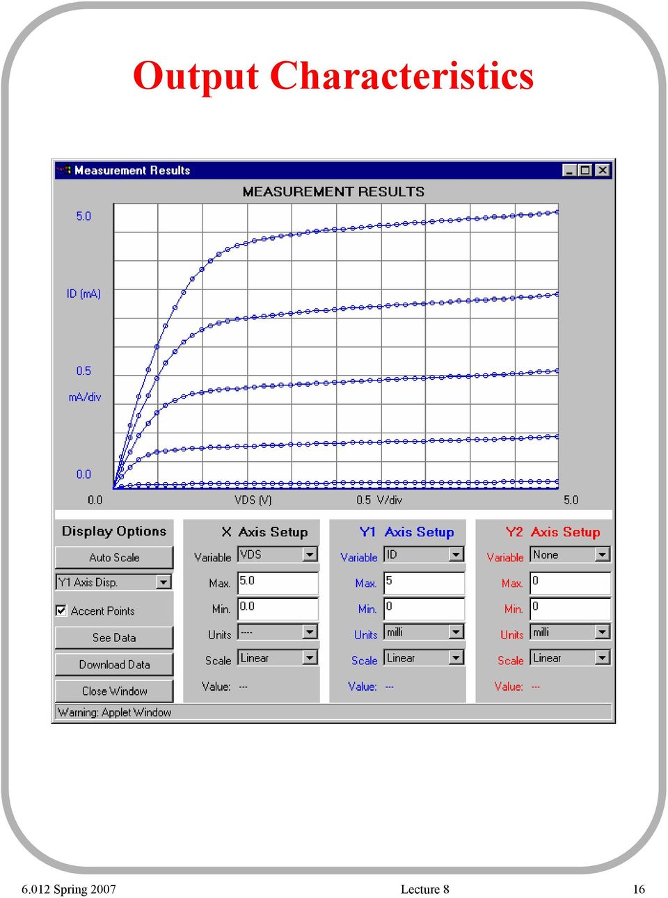
15 I-V Characteristics (Contd.) Output Characteristics Transfer characteristics: Spring 2007 Lecture 8 15

16 Output Characteristics Spring 2007 Lecture 8 16
17 Summary of Key Concepts MOSFET Output Characteristics I-V Characteristics in Cutoff Regime V GS < V T I D = 0 I-V Characteristics in Linear Regime V DS < V GS -V T I D = W L µ nc ox V GS V DS 2 V T I-V Characteristics in Saturation Regime V DS V GS -V T V DS I Dsat = W 2L µ nc ox ( V GS V T ) Spring 2007 Lecture 8 17
 2 6.")
Lecture 9 - MOSFET (I) MOSFET I-V Characteristics. March 6, 2003
 MOSFET I-V Characteristics. March 6, 2003") 6.12 - Microelectronic Devices and Circuits - Spring 23 Lecture 9-1 Lecture 9 - MOSFET (I) MOSFET I-V Characteristics March 6, 23 Contents: 1. MOSFET: cross-section, layout, symbols 2. Qualitative operation
6.12 - Microelectronic Devices and Circuits - Spring 23 Lecture 9-1 Lecture 9 - MOSFET (I) MOSFET I-V Characteristics March 6, 23 Contents: 1. MOSFET: cross-section, layout, symbols 2. Qualitative operation
Lecture 9 - MOSFET (I) MOSFET I-V Characteristics. October 6, 2005
 MOSFET I-V Characteristics. October 6, 2005") 6.12 - Microelectronic Devices and Circuits - Fall 25 Lecture 9-1 Lecture 9 - MOSFET (I) MOSFET I-V Characteristics October 6, 25 Contents: 1. MOSFET: cross-section, layout, symbols 2. Qualitative operation
6.12 - Microelectronic Devices and Circuits - Fall 25 Lecture 9-1 Lecture 9 - MOSFET (I) MOSFET I-V Characteristics October 6, 25 Contents: 1. MOSFET: cross-section, layout, symbols 2. Qualitative operation
Lecture 9 MOSFET(II) MOSFET I-V CHARACTERISTICS(contd.)
 MOSFET I-V CHARACTERISTICS(contd.)") Lecture 9 MOSFET(II) MOSFET I-V CHARACTERISTICS(contd.) Outline 1. The saturation regime 2. Backgate characteristics Reading Assignment: Howe and Sodini, Chapter 4, Section 4.4 Announcements: 1. Quiz#1:
Lecture 9 MOSFET(II) MOSFET I-V CHARACTERISTICS(contd.) Outline 1. The saturation regime 2. Backgate characteristics Reading Assignment: Howe and Sodini, Chapter 4, Section 4.4 Announcements: 1. Quiz#1:
Transconductance. (Saturated) MOSFET Small-Signal Model. The small-signal drain current due to v gs is therefore given by
 MOSFET Small-Signal Model. The small-signal drain current due to v gs is therefore given by") 11 (Saturated) MOSFET Small-Signal Model Transconductance Concept: find an equivalent circuit which interrelates the incremental changes in i D v GS v DS etc. for the MOSFET in saturation The small-signal
11 (Saturated) MOSFET Small-Signal Model Transconductance Concept: find an equivalent circuit which interrelates the incremental changes in i D v GS v DS etc. for the MOSFET in saturation The small-signal
EDC Lesson 12: Transistor and FET Characteristics. 2008 EDCLesson12- ", Raj Kamal, 1
 EDC Lesson 12: Transistor and FET Characteristics Lesson-12: MOSFET (enhancement and depletion mode) Characteristics and Symbols 2008 EDCLesson12- ", Raj Kamal, 1 1. Metal Oxide Semiconductor Field Effect
CO2005: Electronics I (FET) Electronics I, Neamen 3th Ed. 1
 Electronics I, Neamen 3th Ed. 1") CO2005: Electronics I The Field-Effect Transistor (FET) Electronics I, Neamen 3th Ed. 1 MOSFET The metal-oxide-semiconductor field-effect transistor (MOSFET) becomes a practical reality in the 1970s. The
CO2005: Electronics I The Field-Effect Transistor (FET) Electronics I, Neamen 3th Ed. 1 MOSFET The metal-oxide-semiconductor field-effect transistor (MOSFET) becomes a practical reality in the 1970s. The
Bob York. Transistor Basics - MOSFETs
 Bob York Transistor Basics - MOSFETs Transistors, Conceptually So far we have considered two-terminal devices that are described by a current-voltage relationship I=f(V Resistors: Capacitors: Inductors:
Integrated Circuits & Systems
 Federal University of Santa Catarina Center for Technology Computer Science & Electronics Engineering Integrated Circuits & Systems INE 5442 Lecture 11 MOSFET part 2 [email protected] I D -V DS Characteristics
Lecture 090 Large Signal MOSFET Model (3/24/10) Page 090-1
 Page 090-1") Lecture 9 Large Signal MOSFET Model (3/24/1) Page 9-1 LECTURE 9 LARGE SIGNAL MOSFET MODEL LECTURE ORGANIZATION Outline Introduction to modeling Operation of the MOS transistor Simple large signal model
Lecture 9 Large Signal MOSFET Model (3/24/1) Page 9-1 LECTURE 9 LARGE SIGNAL MOSFET MODEL LECTURE ORGANIZATION Outline Introduction to modeling Operation of the MOS transistor Simple large signal model
Lecture 17 The Bipolar Junction Transistor (I) Forward Active Regime
 Forward Active Regime") Lecture 17 The Bipolar Junction Transistor (I) Forward Active Regime Outline The Bipolar Junction Transistor (BJT): structure and basic operation I-V characteristics in forward active regime Reading Assignment:
Lecture 17 The Bipolar Junction Transistor (I) Forward Active Regime Outline The Bipolar Junction Transistor (BJT): structure and basic operation I-V characteristics in forward active regime Reading Assignment:
The MOSFET Transistor
 The MOSFET Transistor The basic active component on all silicon chips is the MOSFET Metal Oxide Semiconductor Field Effect Transistor Schematic symbol G Gate S Source D Drain The voltage on the gate controls
Here we introduced (1) basic circuit for logic and (2)recent nano-devices, and presented (3) some practical issues on nano-devices.
 basic circuit for logic and (2)recent nano-devices, and presented (3) some practical issues on nano-devices.") Outline Here we introduced () basic circuit for logic and (2)recent nano-devices, and presented (3) some practical issues on nano-devices. Circuit Logic Gate A logic gate is an elemantary building block
Outline Here we introduced () basic circuit for logic and (2)recent nano-devices, and presented (3) some practical issues on nano-devices. Circuit Logic Gate A logic gate is an elemantary building block
Notes about Small Signal Model. for EE 40 Intro to Microelectronic Circuits
 Notes about Small Signal Model for EE 40 Intro to Microelectronic Circuits 1. Model the MOSFET Transistor For a MOSFET transistor, there are NMOS and PMOS. The examples shown here would be for NMOS. Figure
Field-Effect (FET) transistors
 transistors") Field-Effect (FET) transistors References: Hayes & Horowitz (pp 142-162 and 244-266), Rizzoni (chapters 8 & 9) In a field-effect transistor (FET), the width of a conducting channel in a semiconductor and,
Field-Effect (FET) transistors References: Hayes & Horowitz (pp 142-162 and 244-266), Rizzoni (chapters 8 & 9) In a field-effect transistor (FET), the width of a conducting channel in a semiconductor and,
AN105. Introduction: The Nature of VCRs. Resistance Properties of FETs
 Introduction: The Nature of s A voltage-controlled resistor () may be defined as a three-terminal variable resistor where the resistance value between two of the terminals is controlled by a voltage potential
MOS Transistors as Switches
 MOS Transistors as Switches G (gate) nmos transistor: Closed (conducting) when Gate = 1 (V DD ) D (drain) S (source) Oen (non-conducting) when Gate = 0 (ground, 0V) G MOS transistor: Closed (conducting)
Chapter 10 Advanced CMOS Circuits
 Transmission Gates Chapter 10 Advanced CMOS Circuits NMOS Transmission Gate The active pull-up inverter circuit leads one to thinking about alternate uses of NMOS devices. Consider the circuit shown in
COMMON-SOURCE JFET AMPLIFIER
 EXPERIMENT 04 Objectives: Theory: 1. To evaluate the common-source amplifier using the small signal equivalent model. 2. To learn what effects the voltage gain. A self-biased n-channel JFET with an AC
Lecture 030 DSM CMOS Technology (3/24/10) Page 030-1
 Page 030-1") Lecture 030 DSM CMOS Technology (3/24/10) Page 030-1 LECTURE 030 - DEEP SUBMICRON (DSM) CMOS TECHNOLOGY LECTURE ORGANIZATION Outline Characteristics of a deep submicron CMOS technology Typical deep submicron
Lecture 030 DSM CMOS Technology (3/24/10) Page 030-1 LECTURE 030 - DEEP SUBMICRON (DSM) CMOS TECHNOLOGY LECTURE ORGANIZATION Outline Characteristics of a deep submicron CMOS technology Typical deep submicron
BJT Ebers-Moll Model and SPICE MOSFET model
 Department of Electrical and Electronic Engineering mperial College London EE 2.3: Semiconductor Modelling in SPCE Course homepage: http://www.imperial.ac.uk/people/paul.mitcheson/teaching BJT Ebers-Moll
LAB 7 MOSFET CHARACTERISTICS AND APPLICATIONS
 LAB 7 MOSFET CHARACTERISTICS AND APPLICATIONS Objective In this experiment you will study the i-v characteristics of an MOS transistor. You will use the MOSFET as a variable resistor and as a switch. BACKGROUND
A Review of MOS Device Physics
 A Review of MOS Device Physics 1.0 Introduction This set of notes focuses on those aspects of transistor behavior that are of immediate relevance to the analog circuit designer. Separation of first order
CHAPTER 10 Fundamentals of the Metal Oxide Semiconductor Field Effect Transistor
 CHAPTER 10 Fundamentals of the Metal Oxide Semiconductor Field Effect Transistor Study the characteristics of energy bands as a function of applied voltage in the metal oxide semiconductor structure known
MOSFET DEVICE MODELING FOR ANALOG CIRCUITS DESIGN
 MOSFET DEVICE MODELING FOR ANALOG CIRCUITS DESIGN Student name: Truong, Long Giang Student #: 970304580 Course: ECE1352F 1. INTRODUCTION The technological trend towards deep sub-micrometer dimensions,
Lecture 23 - Frequency Response of Amplifiers (I) Common-Source Amplifier. December 1, 2005
 Common-Source Amplifier. December 1, 2005") 6.012 Microelectronic Devices and Circuits Fall 2005 Lecture 231 Lecture 23 Frequency Response of Amplifiers (I) CommonSource Amplifier December 1, 2005 Contents: 1. Introduction 2. Intrinsic frequency
6.012 Microelectronic Devices and Circuits Fall 2005 Lecture 231 Lecture 23 Frequency Response of Amplifiers (I) CommonSource Amplifier December 1, 2005 Contents: 1. Introduction 2. Intrinsic frequency
Junction FETs. FETs. Enhancement Not Possible. n p n p n p
 A11 An Introduction to FETs Introduction The basic principle of the field-effect transistor (FET) has been known since J. E. Lilienfeld s patent of 1925. The theoretical description of a FET made by hockley
Fig6-22 CB configuration. Z i [6-54] Z o [6-55] A v [6-56] Assuming R E >> r e. A i [6-57]
![Fig6-22 CB configuration. Z i [6-54] Z o [6-55] A v [6-56] Assuming R E >> r e. A i [6-57]](/thumbs/40/21338705.jpg "Fig6-22 CB configuration. Z i [6-54] Z o [6-55] A v [6-56] Assuming R E >> r e. A i [6-57]") Common-Base Configuration (CB) The CB configuration having a low input and high output impedance and a current gain less than 1, the voltage gain can be quite large, r o in MΩ so that ignored in parallel
Common-Base Configuration (CB) The CB configuration having a low input and high output impedance and a current gain less than 1, the voltage gain can be quite large, r o in MΩ so that ignored in parallel
Small Signal Analysis of a PMOS transistor Consider the following PMOS transistor to be in saturation. Then, 1 2
 Small Signal Analysis of a PMOS transistor Consider the following PMOS transistor to be in saturation. Then, 1 I SD = µ pcox( VSG Vtp)^2(1 + VSDλ) 2 From this equation it is evident that I SD is a function
CONTENTS. Preface. 1.1.2. Energy bands of a crystal (intuitive approach)
") CONTENTS Preface. Energy Band Theory.. Electron in a crystal... Two examples of electron behavior... Free electron...2. The particle-in-a-box approach..2. Energy bands of a crystal (intuitive approach)..3.
CONTENTS Preface. Energy Band Theory.. Electron in a crystal... Two examples of electron behavior... Free electron...2. The particle-in-a-box approach..2. Energy bands of a crystal (intuitive approach)..3.
Power MOSFET Basics Abdus Sattar, IXYS Corporation
 Power MOSFET Basics Abdus Sattar, IXYS Corporation Power MOSFETs have become the standard choice for the main switching devices in a broad range of power conversion applications. They are majority carrier
Understanding Low Drop Out (LDO) Regulators
 Regulators") Understanding Low Drop Out (LDO) Regulators Michael Day, Texas Instruments ABSTRACT This paper provides a basic understanding of the dropout performance of a low dropout linear regulator (LDO). It shows
Understanding Low Drop Out (LDO) Regulators Michael Day, Texas Instruments ABSTRACT This paper provides a basic understanding of the dropout performance of a low dropout linear regulator (LDO). It shows
Field Effect Transistors
 506 19 Principles of Electronics Field Effect Transistors 191 Types of Field Effect Transistors 193 Principle and Working of JFET 195 Importance of JFET 197 JFET as an Amplifier 199 Salient Features of
Fourth generation MOSFET model and its VHDL-AMS implementation
 Fourth generation MOSFET model and its VHDL-AMS implementation Fabien Prégaldiny and Christophe Lallement [email protected] ERM-PHASE, Parc d innovation, BP 10413, 67412 Illkirch
Digital Integrated Circuit (IC) Layout and Design - Week 3, Lecture 5
 Layout and Design - Week 3, Lecture 5") igital Integrated Circuit (IC) Layout and esign - Week 3, Lecture 5! http://www.ee.ucr.edu/~rlake/ee134.html EE134 1 Reading and Prelab " Week 1 - Read Chapter 1 of text. " Week - Read Chapter of text.
igital Integrated Circuit (IC) Layout and esign - Week 3, Lecture 5! http://www.ee.ucr.edu/~rlake/ee134.html EE134 1 Reading and Prelab " Week 1 - Read Chapter 1 of text. " Week - Read Chapter of text.
MOS Transistor 6.1 INTRODUCTION TO THE MOSFET
 Hu_ch06v3.fm Page 195 Friday, February 13, 2009 4:51 PM 6 MOS Transistor CHAPTER OBJECTIVES This chapter provides a comprehensive introduction to the modern MOSFETs in their on state. (The off state theory
W04 Transistors and Applications. Yrd. Doç. Dr. Aytaç Gören
 W04 Transistors and Applications W04 Transistors and Applications ELK 2018 - Contents W01 Basic Concepts in Electronics W02 AC to DC Conversion W03 Analysis of DC Circuits (self and condenser) W04 Transistors
An Introduction to the EKV Model and a Comparison of EKV to BSIM
 An Introduction to the EKV Model and a Comparison of EKV to BSIM Stephen C. Terry 2. 3.2005 Integrated Circuits & Systems Laboratory 1 Overview Characterizing MOSFET operating regions EKV model fundamentals
Application Note AN-940
 Application Note AN-940 How P-Channel MOSFETs Can Simplify Your Circuit Table of Contents Page 1. Basic Characteristics of P-Channel HEXFET Power MOSFETs...1 2. Grounded Loads...1 3. Totem Pole Switching
Power MOSFET Basics By Vrej Barkhordarian, International Rectifier, El Segundo, Ca.
 Power MOFET Basics By Vrej Barkhordarian, International Rectifier, El egundo, Ca. Breakdown Voltage... On-resistance... Transconductance... Threshold Voltage... iode Forward Voltage... Power issipation...
Introduction to VLSI Fabrication Technologies. Emanuele Baravelli
 Introduction to VLSI Fabrication Technologies Emanuele Baravelli 27/09/2005 Organization Materials Used in VLSI Fabrication VLSI Fabrication Technologies Overview of Fabrication Methods Device simulation
A I DM. W/ C V GS Gate-to-Source Voltage ± 20. Thermal Resistance Symbol Parameter Typ. Max. Units
 V DS 2 V V GS Max ± 2 V R DSon) max @V GS = V) 24 m * PD - 9787A HEXFET Power MOSFET R DSon) max @V GS = 4.V) 4 m 6 Micro3 TM SOT-23) Applications) Load System Switch Features and Benefits Features Benefits
5.11 THE JUNCTION FIELD-EFFECT TRANSISTOR (JFET)
") This material is from a previous edition of Microelectronic Circuits. These sections provide valuable information, but please note that the references do not correspond to the 6th or 7th edition of the
This material is from a previous edition of Microelectronic Circuits. These sections provide valuable information, but please note that the references do not correspond to the 6th or 7th edition of the
UNIVERSITY OF CALIFORNIA, BERKELEY College of Engineering Department of Electrical Engineering and Computer Sciences
 UNIVERSITY OF CALIFORNIA, BERKELEY College of Engineering Department of Electrical Engineering and Computer Sciences Elad Alon Homework #4 Solutions EECS141 PROBLEM 1: Shoot-Through Current In this problem,
A I DM. W/ C V GS Gate-to-Source Voltage ± 12. Thermal Resistance Symbol Parameter Typ. Max. Units
 V DS 2 V V GS Max ±2 V * PD - 973A HEXFET Power MOSFET R DSon) max @V GS = 4.V) 2. m R DSon) max @V GS = 2.V) 27. m 6 Micro3 TM SOT-23) Applications) Load System Switch Features and Benefits Features Benefits
Power MOSFET FEATURES. IRF9640PbF SiHF9640-E3 IRF9640 SiHF9640
 Power MOSFET PRODUCT SUMMARY V DS (V) 200 R DS(on) (Ω) = 10 V 0.50 Q g (Max.) (nc) 44 Q gs (nc) 7.1 Q gd (nc) 27 Configuration Single TO220AB G DS ORDERING INFORMATION Package Lead (Pb)free SnPb G S D
N-Channel 20-V (D-S) 175 C MOSFET
 175 C MOSFET") N-Channel -V (D-S) 75 C MOSFET SUD7N-4P PRODUCT SUMMARY V DS (V) r DS(on) ( ) (A) a.37 @ V GS = V 37.6 @ V GS = 4.5 V 9 TO-5 D FEATURES TrenchFET Power MOSFET 75 C Junction Temperature PWM Optimized for
N-Channel -V (D-S) 75 C MOSFET SUD7N-4P PRODUCT SUMMARY V DS (V) r DS(on) ( ) (A) a.37 @ V GS = V 37.6 @ V GS = 4.5 V 9 TO-5 D FEATURES TrenchFET Power MOSFET 75 C Junction Temperature PWM Optimized for
The MOS Transistor in Weak Inversion
 MOFE Operation in eak and Moderate nversion he MO ransistor in eak nversion n this section we will lore the behavior of the MO transistor in the subthreshold regime where the channel is weakly inverted.
RoHS Compliant Containing no Lead, no Bromide and no Halogen. IRF9310PbF SO8 Tube/Bulk 95 IRF9310TRPbF SO8 Tape and Reel 4000
 PD 97437A IRF93PbF HEXFET Power MOSFET V DS 30 V R DS(on) max (@V GS = V) I D (@T A = 25 C) 4. mω 20 A * SO8 Applications Charge and Discharge Switch for Notebook PC Battery Application Features and Benefits
Power MOSFET. IRF510PbF SiHF510-E3 IRF510 SiHF510. PARAMETER SYMBOL LIMIT UNIT Drain-Source Voltage V DS 100 V Gate-Source Voltage V GS ± 20
 Power MOSFET PRODUCT SUMMARY (V) 100 R DS(on) () = 0.54 Q g max. (nc) 8.3 Q gs (nc) 2.3 Q gd (nc) 3.8 Configuration Single D TO220AB G FEATURES Dynamic dv/dt rating Available Repetitive avalanche rated
Depletion-Mode Power MOSFETs and Applications Abdus Sattar, IXYS Corporation
 epletion-mode Power MOSFETs and Applications Abdus Sattar, XYS Corporation Applications like constant current sources, solid-state relays, telecom switches and high voltage C lines in power systems require
Power MOSFET FEATURES. IRF610PbF SiHF610-E3 IRF610 SiHF610. PARAMETER SYMBOL LIMIT UNIT Drain-Source Voltage V DS 200 V Gate-Source Voltage V GS ± 20
 Power MOSFET PRODUCT SUMMARY (V) 00 R DS(on) ( ) = 1.5 Q g (Max.) (nc) 8. Q gs (nc) 1.8 Q gd (nc) 4.5 Configuration Single FEATURES Dynamic dv/dt Rating Repetitive Avalanche Rated Fast Switching Ease of
IRF150 [REF:MIL-PRF-19500/543] 100V, N-CHANNEL. Absolute Maximum Ratings
![IRF150 [REF:MIL-PRF-19500/543] 100V, N-CHANNEL. Absolute Maximum Ratings](/thumbs/40/21333646.jpg "IRF150 [REF:MIL-PRF-19500/543] 100V, N-CHANNEL. Absolute Maximum Ratings") PD - 90337G REPETITIVE AVALANCHE AND dv/dt RATED HEXFET TRANSISTORS THRU-HOLE (TO-204AA/AE) Product Summary Part Number BVDSS RDS(on) ID IRF150 100V 0.055Ω 38A IRF150 JANTX2N6764 JANTXV2N6764 [REF:MIL-PRF-19500/543]
PD - 90337G REPETITIVE AVALANCHE AND dv/dt RATED HEXFET TRANSISTORS THRU-HOLE (TO-204AA/AE) Product Summary Part Number BVDSS RDS(on) ID IRF150 100V 0.055Ω 38A IRF150 JANTX2N6764 JANTXV2N6764 [REF:MIL-PRF-19500/543]
Power MOSFET. IRF9520PbF SiHF9520-E3 IRF9520 SiHF9520. PARAMETER SYMBOL LIMIT UNIT Drain-Source Voltage V DS - 100 V Gate-Source Voltage V GS ± 20
 Power MOSFET PRODUCT SUMMARY (V) 100 R DS(on) ( ) = 10 V 0.60 Q g (Max.) (nc) 18 Q gs (nc) 3.0 Q gd (nc) 9.0 Configuration Single TO220AB G DS ORDERING INFORMATION Package Lead (Pb)free SnPb G S D PChannel
Power MOSFET FEATURES. IRF740PbF SiHF740-E3 IRF740 SiHF740. PARAMETER SYMBOL LIMIT UNIT Drain-Source Voltage V DS 400 V Gate-Source Voltage V GS ± 20
 Power MOSFET PRODUCT SUMMARY (V) 400 R DS(on) (Ω) = 0.55 Q g (Max.) (nc) 63 Q gs (nc) 9.0 Q gd (nc) 3 Configuration Single FEATURES Dynamic dv/dt Rating Repetitive Avalanche Rated Fast Switching Ease of
Winbond W2E512/W27E257 EEPROM
 Construction Analysis Winbond W2E512/W27E257 EEPROM Report Number: SCA 9703-533 Global Semiconductor Industry the Serving Since 1964 15022 N. 75th Street Scottsdale, AZ 85260-2476 Phone: 602-998-9780 Fax:
Basic FET Ampli ers 6.0 PREVIEW 6.1 THE MOSFET AMPLIFIER
 C H A P T E R 6 Basic FET Ampli ers 6.0 PREVIEW In the last chapter, we described the operation of the FET, in particular the MOSFET, and analyzed and designed the dc response of circuits containing these
Power MOSFET FEATURES. IRFZ44PbF SiHFZ44-E3 IRFZ44 SiHFZ44 T C = 25 C
 Power MOSFET PRODUCT SUMMARY (V) 60 R DS(on) (Ω) V GS = 10 V 0.028 Q g (Max.) (nc) 67 Q gs (nc) 18 Q gd (nc) 25 Configuration Single FEATURES Dynamic dv/dt Rating 175 C Operating Temperature Fast Switching
Features. Description. Table 1. Device summary. Order code Marking Package Packing. STP110N8F6 110N8F6 TO-220 Tube
 N-channel 80 V, 0.0056 Ω typ.,110 A, STripFET F6 Power MOSFET in a TO-220 package Features Datasheet - production data Order code V DS R DS(on)max I D P TOT TAB STP110N8F6 80 V 0.0065 Ω 110 A 200 W TO-220
N-Channel 40-V (D-S) 175 C MOSFET
 175 C MOSFET") N-Channel 4-V (D-S) 75 C MOSFET SUP/SUB85N4-4 PRODUCT SUMMARY V (BR)DSS (V) r DS(on) ( ) (A) 4.4 @ V GS = V 85 a TO-22AB D TO-263 G DRAIN connected to TAB G D S Top View Ordering Information SUP85N4-4
N-Channel 4-V (D-S) 75 C MOSFET SUP/SUB85N4-4 PRODUCT SUMMARY V (BR)DSS (V) r DS(on) ( ) (A) 4.4 @ V GS = V 85 a TO-22AB D TO-263 G DRAIN connected to TAB G D S Top View Ordering Information SUP85N4-4
Power MOSFET FEATURES. IRL540PbF SiHL540-E3 IRL540 SiHL540
 Power MOSFET PRODUCT SUMMARY (V) 100 R DS(on) (Ω) = 5.0 V 0.077 Q g (Max.) (nc) 64 Q gs (nc) 9.4 Q gd (nc) 27 Configuration Single TO220AB G DS ORDERING INFORMATION Package Lead (Pb)free SnPb G D S NChannel
DE275-102N06A RF Power MOSFET
 N-Channel Enhancement Mode Low Q g and R g High dv/dt Nanosecond Switching Ideal for Class C, D, & E Applications Symbol Test Conditions Maximum Ratings V DSS T J = 25 C to 150 C 00 V V DGR T J = 25 C
P-Channel 20 V (D-S) MOSFET
 MOSFET") Si30CDS P-Channel 0 V (D-S) MOSFET MOSFET PRODUCT SUMMARY V DS (V) R DS(on) ( ) I D (A) a Q g (Typ.) - 0 0. at V GS = - 4.5 V - 3. 0.4 at V GS = -.5 V -.7 3.3 nc TO-36 (SOT-3) FEATURES Halogen-free According
Si30CDS P-Channel 0 V (D-S) MOSFET MOSFET PRODUCT SUMMARY V DS (V) R DS(on) ( ) I D (A) a Q g (Typ.) - 0 0. at V GS = - 4.5 V - 3. 0.4 at V GS = -.5 V -.7 3.3 nc TO-36 (SOT-3) FEATURES Halogen-free According
P-Channel 20-V (D-S) MOSFET
 MOSFET") Si33DS P-Channel -V (D-S) MOSFET PRODUCT SUMMARY V DS (V) R DS(on) (Ω) I D (A).39 at V GS = -.5 V -.7 -.5 at V GS = -.5 V -..68 at V GS = -.8 V - 3.5 FEATURES Halogen-free According to IEC 69-- Available
Si33DS P-Channel -V (D-S) MOSFET PRODUCT SUMMARY V DS (V) R DS(on) (Ω) I D (A).39 at V GS = -.5 V -.7 -.5 at V GS = -.5 V -..68 at V GS = -.8 V - 3.5 FEATURES Halogen-free According to IEC 69-- Available
IRF740 N-CHANNEL 400V - 0.46Ω - 10A TO-220 PowerMESH II MOSFET
 N-CHANNEL 400V - 0.46Ω - 10A TO-220 PowerMESH II MOSFET TYPE V DSS R DS(on) I D IRF740 400 V < 0.55 Ω 10 A TYPICAL R DS (on) = 0.46Ω EXCEPTIONAL dv/dt CAPABILITY 100% AVALANCHE TESTED LOW GATE CHARGE VERY
Power MOSFET FEATURES. IRF740PbF SiHF740-E3 IRF740 SiHF740. PARAMETER SYMBOL LIMIT UNIT Drain-Source Voltage V DS 400 V Gate-Source Voltage V GS ± 20
 Power MOSFET PRODUCT SUMMARY (V) 400 R DS(on) (Ω) = 0.55 Q g (Max.) (nc) 63 Q gs (nc) 9.0 Q gd (nc) 3 Configuration Single FEATURES Dynamic dv/dt Rating Repetitive Avalanche Rated Fast Switching Ease of
Power MOSFET FEATURES. IRF540PbF SiHF540-E3 IRF540 SiHF540. PARAMETER SYMBOL LIMIT UNIT Drain-Source Voltage V DS 100 V Gate-Source Voltage V GS ± 20
 Power MOSFET PRODUCT SUMMARY (V) 100 R DS(on) ( ) = 0.077 Q g (Max.) (nc) 72 Q gs (nc) 11 Q gd (nc) 32 Configuration Single TO220AB G DS ORDERING INFORMATION Package Lead (Pb)free SnPb G D S NChannel MOSFET
IRF5305PbF. HEXFET Power MOSFET V DSS = -55V. R DS(on) = 0.06Ω I D = -31A
 = 0.06Ω I D = -31A") dvanced Process Technology Dynamic dv/dt Rating 75 C Operating Temperature Fast Switching PChannel Fully valanche Rated LeadFree Description Fifth Generation HEXFETs from International Rectifier utilize
dvanced Process Technology Dynamic dv/dt Rating 75 C Operating Temperature Fast Switching PChannel Fully valanche Rated LeadFree Description Fifth Generation HEXFETs from International Rectifier utilize
Features. P-Channel Enhancement Mode MOSFET
 P-Channel Enhancement Mode MOSFET Features Pin Description -4V/-25, R DS(ON) = 4mΩ (typ.) @ V GS = -V R DS(ON) = 55mΩ (typ.) @ V GS = -5V Super High Dense Cell Design G D S Reliable and Rugged Lead Free
Sheet Resistance = R (L/W) = R N ------------------ L
 = R N ------------------ L") Sheet Resistance Rewrite the resistance equation to separate (L / W), the length-to-width ratio... which is the number of squares N from R, the sheet resistance = (σ n t) - R L = -----------------------
Sheet Resistance Rewrite the resistance equation to separate (L / W), the length-to-width ratio... which is the number of squares N from R, the sheet resistance = (σ n t) - R L = -----------------------
Introduction to VLSI design (EECS 467)
") Introduction to VLSI design (EECS 467) Proect Short-Channel Effects in MOSFETs December 11 th, Fabio D gostino Daniele Quercia - 1 - Short-Channel Devices MOSFET device is considered to be short when the
Introduction to VLSI design (EECS 467) Proect Short-Channel Effects in MOSFETs December 11 th, Fabio D gostino Daniele Quercia - 1 - Short-Channel Devices MOSFET device is considered to be short when the
3. Diodes and Diode Circuits. 3. Diodes and Diode Circuits TLT-8016 Basic Analog Circuits 2005/2006 1
 3. Diodes and Diode Circuits 3. Diodes and Diode Circuits TLT-8016 Basic Analog Circuits 2005/2006 1 3.1 Diode Characteristics Small-Signal Diodes Diode: a semiconductor device, which conduct the current
MOSFET N-channel enhancement switching transistor IMPORTANT NOTICE. http://www.philips.semiconductors.com use http://www.nxp.com
 Rev. 3 21 November 27 Product data sheet Dear customer, IMPORTANT NOTICE As from October 1st, 26 Philips Semiconductors has a new trade name - NXP Semiconductors, which will be used in future data sheets
AN-9010 MOSFET Basics
 www.fairchildsemi.com AN-9010 MOSFET Basics Summary The Bipolar Power Transistor (BPT), as a switching device for power applications, had a few disadvantages. This led to the development of the power Metal
SIPMOS Small-Signal-Transistor
 SIPMOS Small-Signal-Transistor Features N-channel Depletion mode dv /dt rated Product Summary V DS V R DS(on),max 3.5 Ω I DSS,min.4 A Available with V GS(th) indicator on reel Pb-free lead plating; RoHS
Lecture 30: Biasing MOSFET Amplifiers. MOSFET Current Mirrors.
 Whites, EE 320 Lecture 30 Page 1 of 8 Lecture 30: Biasing MOSFET Amplifiers. MOSFET Current Mirrors. There are two different environments in which MOSFET amplifiers are found, (1) discrete circuits and
Introduction to CMOS VLSI Design
 Introduction to CMOS VLSI esign Slides adapted from: N. Weste,. Harris, CMOS VLSI esign, Addison-Wesley, 3/e, 24 Introduction Integrated Circuits: many transistors on one chip Very Large Scale Integration
N-Channel 100 V (D-S) MOSFET
 MOSFET") Si4DS N-Channel V (D-S) MOSFET MOSFET PRODUCT SUMMARY V DS (V) R DS(on) ( ) I D (A) a Q g (Typ.).4 at V GS = V..67 at V GS = 6 V..9 nc.78 at V GS = 4.5 V.7 FEATURES TrenchFET Power MOSFET % R g Tested
Si4DS N-Channel V (D-S) MOSFET MOSFET PRODUCT SUMMARY V DS (V) R DS(on) ( ) I D (A) a Q g (Typ.).4 at V GS = V..67 at V GS = 6 V..9 nc.78 at V GS = 4.5 V.7 FEATURES TrenchFET Power MOSFET % R g Tested
Power MOSFET FEATURES. IRF520PbF SiHF520-E3 IRF520 SiHF520. PARAMETER SYMBOL LIMIT UNIT Drain-Source Voltage V DS 100 V Gate-Source Voltage V GS ± 20
 Power MOSFET PRODUCT SUMMARY (V) 100 R DS(on) ( ) = 0.7 Q g (Max.) (nc) 16 Q gs (nc) 4.4 Q gd (nc) 7.7 Configuration Single TO0AB G DS ORDERING INFORMATION Package Lead (Pb)free SnPb G D S NChannel MOSFET
P-Channel 1.25-W, 1.8-V (G-S) MOSFET
 MOSFET") Si5DS P-Channel.5-W,.-V (G-S) MOSFET PRODUCT SUMMARY V DS (V) R DS(on) (Ω) I D (A).5 at V GS = -.5 V ±.5 -.7 at V GS = -.5 V ±. at V GS = -. V ± FEATURES Halogen-free According to IEC 9-- Available TrenchFET
Si5DS P-Channel.5-W,.-V (G-S) MOSFET PRODUCT SUMMARY V DS (V) R DS(on) (Ω) I D (A).5 at V GS = -.5 V ±.5 -.7 at V GS = -.5 V ±. at V GS = -. V ± FEATURES Halogen-free According to IEC 9-- Available TrenchFET
Module 7 : I/O PADs Lecture 33 : I/O PADs
 Module 7 : I/O PADs Lecture 33 : I/O PADs Objectives In this lecture you will learn the following Introduction Electrostatic Discharge Output Buffer Tri-state Output Circuit Latch-Up Prevention of Latch-Up
STW20NM50 N-CHANNEL 550V @ Tjmax - 0.20Ω - 20ATO-247 MDmesh MOSFET
 N-CHANNEL 550V @ Tjmax - 0.20Ω - 20ATO-247 MDmesh MOSFET TYPE V DSS (@Tjmax) R DS(on) I D STW20NM50 550V < 0.25Ω 20 A TYPICAL R DS (on) = 0.20Ω HIGH dv/dt AND AVALANCHE CAPABILITIES 100% AVALANCHE TESTED
Application Note AN-1070
 Application Note AN-1070 Class D Audio Amplifier Performance Relationship to MOSFET Parameters By Jorge Cerezo, International Rectifier Table of Contents Page Abstract... 2 Introduction... 2 Key MOSFET
C Soldering Temperature, for 10 seconds 300 (1.6mm from case )
") dvanced Process Technology Dynamic dv/dt Rating 75 C Operating Temperature Fast Switching Fully valanche Rated Lead-Free Description Fifth Generation HEXFETs from International Rectifier utilize advanced
dvanced Process Technology Dynamic dv/dt Rating 75 C Operating Temperature Fast Switching Fully valanche Rated Lead-Free Description Fifth Generation HEXFETs from International Rectifier utilize advanced
V DSS R DS(on) max Qg. 30V 3.2mΩ 36nC
 max Qg. 30V 3.2mΩ 36nC") PD - 96232 Applications l Optimized for UPS/Inverter Applications l High Frequency Synchronous Buck Converters for Computer Processor Power l High Frequency Isolated DC-DC Converters with Synchronous Rectification
PD - 96232 Applications l Optimized for UPS/Inverter Applications l High Frequency Synchronous Buck Converters for Computer Processor Power l High Frequency Isolated DC-DC Converters with Synchronous Rectification
200V, N-CHANNEL. Absolute Maximum Ratings. Features: www.irf.com 1 PD - 90370
 PD - 90370 REPETITIVE AVALANCHE AND dv/dt RATED HEXFET TRANSISTORS THRU-HOLE (TO-204AA/AE) IRF240 200V, N-CHANNEL Product Summary Part Number BVDSS RDS(on) ID IRF240 200V 0.18Ω 18A The HEXFET technology
IRF6201PbF. HEXFET Power MOSFET V DS 20 V. R DS(on) max. 2.75 mω. Q g (typical) 130 nc 27 A. Absolute Maximum Ratings
 max. 2.75 mω. Q g (typical) 130 nc 27 A. Absolute Maximum Ratings") PD - 97500A IRF620PbF V DS 20 V HEXFET Power MOSFET R DS(on) max (@ = 4.5V) 2.45 mω 6 R DS(on) max (@ = 2.5V) 2.75 mω 6 6 Q g (typical) 30 nc * SO-8 I D (@T A = 25 C) 27 A Applications OR-ing or hot-swap
PD - 97500A IRF620PbF V DS 20 V HEXFET Power MOSFET R DS(on) max (@ = 4.5V) 2.45 mω 6 R DS(on) max (@ = 2.5V) 2.75 mω 6 6 Q g (typical) 30 nc * SO-8 I D (@T A = 25 C) 27 A Applications OR-ing or hot-swap
N-Channel 60-V (D-S), 175 C MOSFET
, 175 C MOSFET") N-Channel 6-V (D-S), 75 C MOSFET SUP/SUB7N6-4 V (BR)DSS (V) r DS(on) ( ) (A) 6.4 7 a TO-22AB D TO-263 DRAIN connected to TAB G G D S Top View SUP7N6-4 G D S Top View SUB7N6-4 S N-Channel MOSFET Parameter
N-Channel 6-V (D-S), 75 C MOSFET SUP/SUB7N6-4 V (BR)DSS (V) r DS(on) ( ) (A) 6.4 7 a TO-22AB D TO-263 DRAIN connected to TAB G G D S Top View SUP7N6-4 G D S Top View SUB7N6-4 S N-Channel MOSFET Parameter
Intel s Revolutionary 22 nm Transistor Technology
 Intel s Revolutionary 22 nm Transistor Technology Mark Bohr Intel Senior Fellow Kaizad Mistry 22 nm Program Manager May, 2011 1 Key Messages Intel is introducing revolutionary Tri-Gate transistors on its
IRFP460LC PD - 9.1232. HEXFET Power MOSFET V DSS = 500V. R DS(on) = 0.27Ω I D = 20A
 = 0.27Ω I D = 20A") HEXFET Power MOSFET PD - 9.232 IRFP460LC Ultra Low Gate Charge Reduced Gate Drive Requirement Enhanced 30V V gs Rating Reduced C iss, C oss, C rss Isolated Central Mounting Hole Dynamic dv/dt Rated Repetitive
HEXFET Power MOSFET PD - 9.232 IRFP460LC Ultra Low Gate Charge Reduced Gate Drive Requirement Enhanced 30V V gs Rating Reduced C iss, C oss, C rss Isolated Central Mounting Hole Dynamic dv/dt Rated Repetitive
N-Channel 60-V (D-S) MOSFET
 MOSFET") 7/7, VQJ/P, BS7 -Channel 6-V (D-S) MOSFET Part umber V (BR)DSS Min (V) r DS(on) Max ( ) V GS(th) (V) I D (A) 7 5 @ V GS = V.8 to. 7 7.5 @ V GS = V to.5.5 VQJ 6 5.5 @ V GS = V.8 to.5.5 VQP 5.5 @ V GS =
7/7, VQJ/P, BS7 -Channel 6-V (D-S) MOSFET Part umber V (BR)DSS Min (V) r DS(on) Max ( ) V GS(th) (V) I D (A) 7 5 @ V GS = V.8 to. 7 7.5 @ V GS = V to.5.5 VQJ 6 5.5 @ V GS = V.8 to.5.5 VQP 5.5 @ V GS =
P-Channel 60 V (D-S) MOSFET
 MOSFET") TP6K P-Channel 6 V (D-S) MOSFET G S PRODUCT SUMMARY V DS (V) R DS(on) ( ) V GS(th) (V) I D (ma) - 6 6 at V GS = - V - to - - 85 TO-6 (SOT-) Top View D Marking Code: 6Kwll 6K = Part Number Code for TP6K
TP6K P-Channel 6 V (D-S) MOSFET G S PRODUCT SUMMARY V DS (V) R DS(on) ( ) V GS(th) (V) I D (ma) - 6 6 at V GS = - V - to - - 85 TO-6 (SOT-) Top View D Marking Code: 6Kwll 6K = Part Number Code for TP6K
Fabrication and Characterization of N- and P-Type a-si:h Thin Film Transistors
 Fabrication and Characterization of N- and P-Type a-si:h Thin Film Transistors Engineering Practical Jeffrey Frederick Gold Fitzwilliam College University of Cambridge Lent 1997 FABRCATON AND CHARACTERZATON
CHAPTER 2 POWER AMPLIFIER
 CHATER 2 OWER AMLFER 2.0 ntroduction The main characteristics of an amplifier are Linearity, efficiency, output power, and signal gain. n general, there is a trade off between these characteristics. For
ENEE 313, Spr 09 Midterm II Solution
 ENEE 313, Spr 09 Midterm II Solution PART I DRIFT AND DIFFUSION, 30 pts 1. We have a silicon sample with non-uniform doping. The sample is 200 µm long: In the figure, L = 200 µm= 0.02 cm. At the x = 0
IRLR8743PbF IRLU8743PbF HEXFET Power MOSFET
 Applications l High Frequency Synchronous Buck Converters for Computer Processor Power l High Frequency Isolated DC-DC Converters with Synchronous Rectification for Telecom and Industrial Use l Lead-Free
OptiMOS 3 Power-Transistor
 Type IPD6N3L G OptiMOS 3 Power-Transistor Features Fast switching MOSFET for SMPS Optimized technology for DC/DC converters Qualified according to JEDEC 1) for target applications Product Summary V DS
05 Bipolar Junction Transistors (BJTs) basics
 basics") The first bipolar transistor was realized in 1947 by Brattain, Bardeen and Shockley. The three of them received the Nobel prize in 1956 for their invention. The bipolar transistor is composed of two PN
The first bipolar transistor was realized in 1947 by Brattain, Bardeen and Shockley. The three of them received the Nobel prize in 1956 for their invention. The bipolar transistor is composed of two PN
Advanced VLSI Design CMOS Processing Technology
 Isolation of transistors, i.e., their source and drains, from other transistors is needed to reduce electrical interactions between them. For technologies