Fig6-22 CB configuration. Z i [6-54] Z o [6-55] A v [6-56] Assuming R E >> r e. A i [6-57]
|
|
|
- Camron Jenkins
- 7 years ago
- Views:
Transcription
1 Common-Base Configuration (CB) The CB configuration having a low input and high output impedance and a current gain less than 1, the voltage gain can be quite large, r o in MΩ so that ignored in parallel with R C Z i Fig6-22 CB configuration Fig6-23 r e equivalent circuit Z o [6-54] A v [6-55] A i Assuming R E >> r e [6-56] [6-57] Phase Relationship: the resulting equation for the A v is a positive reveals that the output V o and input V i are in phase for the common-base configuration Example 8: For the network in fig 6-24 Solution: I E Fig6-24 Ex 8 114
![Z o [6-54] A v [6-55] A i Assuming R E >> r e [6-56] [6-57] Phase Relationship: the resulting equation for the A v is a positive reveals](/docs-images/46/21338705/images/page_1.jpg "that the output V o and input V i are in phase for the common-base configuration Example 8: For the network in fig 6-24 Solution: I E")
2 r e Z i Z o A v A i Collector Feedback Configuration (CE A feedback path from collector to base increased the stability of the system Z i Fig6-25 feedback configuration Fig6-26 r e model into network of fig

3 [6-58] Z o to define Z o set V i to zero, the effect of βre is removed and R F appears in parallel with R C [6-59] A v at node C of Fig 6-26 A i Applying KVL around the outside network loop [6-60] 116
![parallel with R C [6-59] A v at node C of Fig](/docs-images/46/21338705/images/page_3.jpg "6-26 A i Applying KVL around the outside network")
4 Ignoring βr e compared to R F and βr C gives us βr C >> R F [6-61] [6-62] Phase Relationship: the negative sign in the resulting equation for the A v reveals that a 180 º phase shift occurs between the output V O and input V i Example 9: For the network of fig6-27 determine Solution: I B Fig6-27 Example 9: I E r e Z i Z o A v A i 117

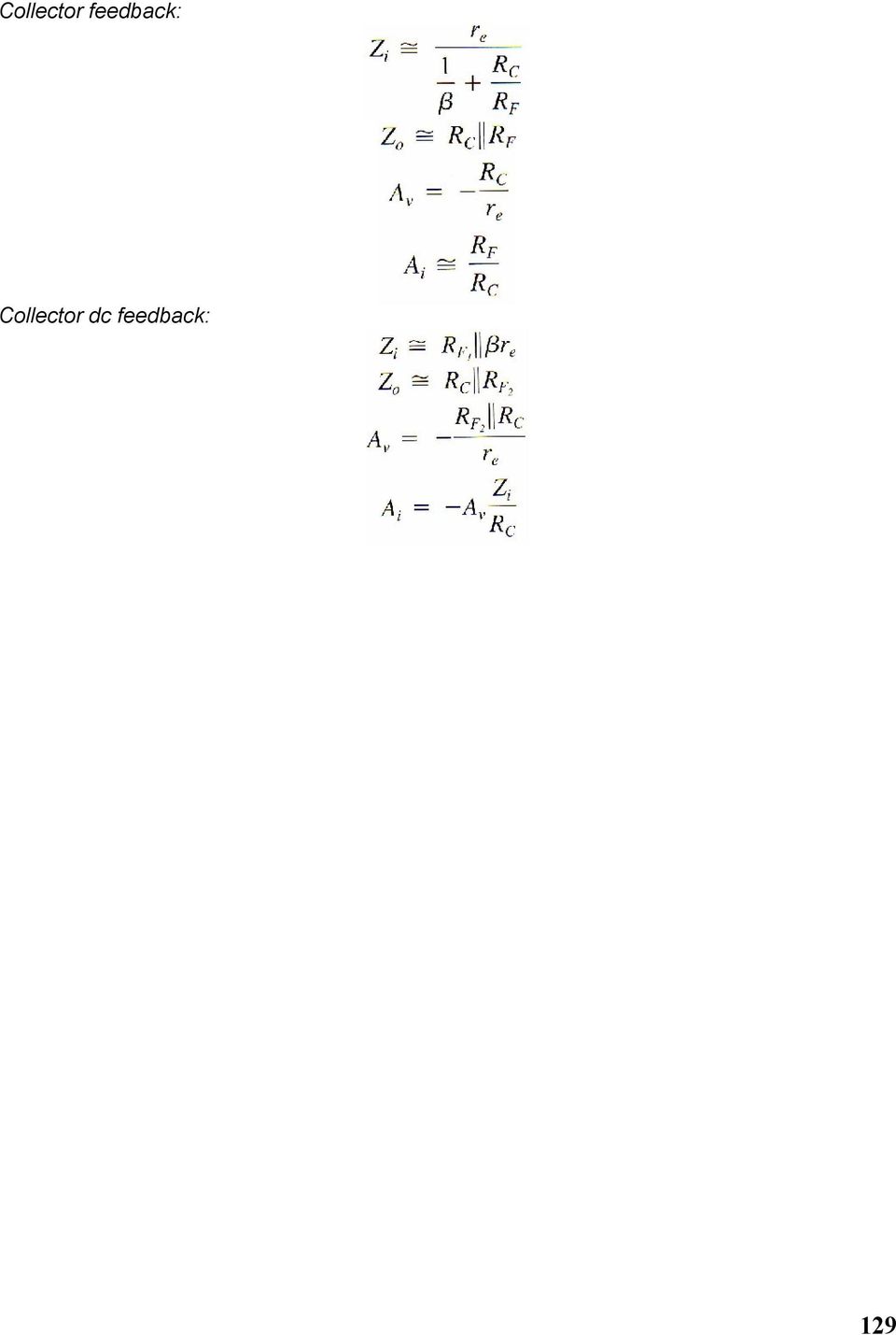
5 For the configuration of Fig6-28, will determine the variables Z i Fig6-28 Collector feedback configuration Z o [6-63] A v [6-64] [6-65] A i [6-66] Collector DC feedback Configuration (CE) The dc feedback resistor increased stability; C 3 will shift portions of the feedback resistance to the input and output sections of the network in the ac domain. Zi Fig6-29 Collector dc feedback Fig6-30 r e equivalent circuit of the network Z o [6-67] For r o 10R C [6-68] 118

6 A v [6-69] For r o 10R C [6-70] A i for the input side [6-71] [6-72] [6-73] Or [6-74] Phase Relationship: the negative sign in the resulting equation for the A v reveals that a 180 º phase shift occurs between the output V O and input V i 119

7 Example 10: For the network of fig6-31 determine: Solution: DC testing: I B Fig6-31 Example 10 I E r e βr e Z i F ig6-32 r e equivalent Testing the condition r o 10R C we find So Z o It is satisfied 120

8 Approximate Hybrid Equivalent Circuit Fig6-33 Approximate CE hybrid circuit Fig 6-34 Approximate CB hybrid circuit h ie = βr e h fe =β h oe = 1/r o h fb = -α h ib =r e Fixed-Bias Configuration (CE) Fig 6-35fixed-bias configuration Fig6-36 approximate hybrid equivalent circuit Z i Z o [6-75] A v [6-76] [6-77] A i Assuming that R B >> h ie and 1/ h oe 10R C, then I b Ii and I O = I C = h fe I b = h fe Ii with [6-78] Example 11: For the network of fig6-37, determine 121
![Fig6-36 approximate hybrid equivalent circuit Z i Z o [6-75] A v [6-76] [6-77] A i Assuming that R B >> h ie and 1/ h](/docs-images/46/21338705/images/page_8.jpg "oe 10R C, then I b Ii and I O = I C = h fe I b = h fe Ii with [6-78] Example 11: For the network of fig6-37,")
9 Solution: Fig6-37 Example 11: Voltage-Divider Configuration (CE bypassed) Z i R B =R' Fig6-38Voltage-dividerbiasconfiguration Z o [6-79] A v [6-80] A i [6-81] [6-82] Unbypassed Emitter-Bias Configuration (CE) βr e replaced by h ie and βi b by h fe I b. The analysis will proceed in the manner 122
![A i [6-81] [6-82] Unbypassed Emitter-Bias Configuration (CE) βr e](/docs-images/46/21338705/images/page_9.jpg "replaced by h ie and βi b by h fe I b.")
10 Z i : Fig6-39 CE unbypassed emitter-bias configuration [6-83] Z o [6-84] [6-89] A v And [6-90] A i [6-91] or [6-92] Emitter-Follower Configuration (CE) βr e = h ie and β = h fe, the resulting equations will therefore be quite similar. Z i Fig6-40Emitter-follower configuration [6-93] 123

11 [6-94] Z o the output network will appear as shown in fig A v [6-95] A i [6-96] [6-97] or [6-98 ] Common-Base Configuration (CB) Fig6-41 CB configuration Fig6-42 CB hybrid equivalent circuit Z i Z o [6-99] [6-100] 124

12 A v A i [6-101] [6-102] Example 12: For the network of fig6-43, determine: Solution; Fig 6-43 Example

13 Table6-1 Relative Levels for the Important Parameters of the CE, CB, and CC Transistor Amplifier 126

14 SUMMARY Important Conclusions and Concepts 1. The r e model for a BJT in the ac domain is sensitive to the actual dc operating conditions of the network. This parameter is normally not provided on a specification sheet, although h ie of the normally provided hybrid parameters is equal to β r e but only under specific operating conditions. 2. Most specification sheets for BJT include a list of hybrid parameters to establish an ac model for the transistor. One must be aware, however, that they are provided for a particular set of dc operating conditions. 3. The CE fixed-bias configuration can have a significant voltage gain characteristic, although its input impedance can be relatively low. The approximate current gain is given by simply beta, and the output impedance is normally assumed to be R c. 4. The voltage-divider bias configuration has a higher stability than the fixed-bias configuration, but it has about the same voltage gain, current gain, and output impedance. Due to the biasing resistors, its input impedance may be lower than that of the fixed-bias configuration. 5. The CE emitter-bias configuration with an unbypassed emitter resistor has a larger input resistance than the bypassed configuration, but it will have a much smaller voltage gain than the bypassed configuration. For the unbypassed or by-passed situation, the output impedance is normally assumed to be simply R c. 6. The emitter-follower configuration will always have an output voltage slightly less than the input signal. However, the input impedance can be very large, making it very useful for situations where a high-input first stage is needed to "pick up "as much of the applied signal as possible. Its output impedance is extremely low, making it an excellent signal source for the second stage of a multistage amplifier. 7. The common-base configuration has very low input impedance, but it can have a significant voltage gain. The current gain is just less than 1, and the output impedance is simply R c 8. The collector feedback configuration has input impedance that is sensitive to beta and that can be quite low depending on the parameters of the configuration. However, the voltage gain can be significant and the current gain of some magnitude if the parameters are chosen properly. The output impedance is most often simply the collector resistance R c 9. The collector dc feedback configuration utilizes the dc feedback to increase its stability and the changing state of a capacitor from dc to ac to establish a higher voltage gain than obtained with a straight feedback connection. The output impedance is usually close to R c and the input impedance relatively close to that obtained with the basic common-emitter configuration. 10. The approximate hybrid equivalent network is very similar in composition to that used with the re model. In fact, the same methods of analysis can be applied to both models. For the hybrid model the results will be in terms of the network parameters and the hybrid parameters, whereas for the re model they will be in terms of the network parameters and β, r e and r o 11. The hybrid model for common-emitter, common-base, and common-collector configurations is the same. The only difference will be the magnitude of the parameters of the equivalent network. 127

15 12. for BJT amplifiers that fail to operate properly, the first step should to be checking the dc level and be sure that they support the dc operation of the design. 13. Always keep in mind that capacitors are typically open circuits for the dc analysis and operation and essentially short circuits for the ac response Equations CE fixed bias: CE Voltage-divider bias: CE emitter-bias: Emitter-follower: Common-base: 128

16 Collector feedback: Collector dc feedback: 129
17 7-Felid Effect Transistor (FET) BJT is a current-controlled device; that is I B controls I C. The FET is a voltage-controlled device in which the voltage gate V G controls current through the device. FET is a three-terminal device containing one p-n junction built as either a Junction FET (JFET) or a Metal-Oxide Semiconductor FET (MOS-FET). Construction and Characteristics of JFETS JFET is a type of FET that operates with a reverse biased junction to control current in the channel. JFETs either n channel or p channel Fig7-1 basic structure of the two types of JFET Fig7-2Water analogy for the JFET control mechanism JFET Symbols Notice that the arrow on the gate points "in" for n-channel and "out" for-p channel. Fig7-3 JFET symbols (a) n-channel (b) p-channel JFET Characteristics First consider the case where the V GS = 0V fig7-4a as V DD (and thus V DS ) is increased from 0V, I D will increase proportionally (Fig7-4b between points A and B), this region is called the ohmic region because V DS and I D are related by Ohm's law. Point B in Fig7-4b I D becomes constant. As V DS increases from point B to point C, the reversebias voltage in V GD produces a depletion region large enough to offset the increase in V DS, thus keeping I D relatively constant. Pinch-Off Voltage V P : is the value of V DS at which I D becomes constant and V GS = 0V, a continued increase in V DS above the V P voltage produces a constant drain current I DSS (Drain to Source current with gate sorted) I DSS : is the maximum drain current and is always specified on JFET data sheets, is defined by the condition V GS = 0V and V DS > V P Breakdown: occurs at point C when I D begins to increase very rapidly with any further increase in V DS, Breakdown result damage to the device, so JFETs are always operated below breakdown ( between B & C). V GS Controls I D : Connect a bias voltage V GG, as V GS is set to increasingly more negative values by adjusting V GG, I D decreases. 130

18 Fig 7-4 the drain characteristic curve of a JFET for V GS = 0 V, (pinch-off) Fig7-5 pinch-off occurs at a lower V DS as V GS is increased to more negative values Cutoff Voltage V GS(off) : the value of V GS that makes I D approximately zero,jfet must be operated between V GS = 0V and V GS(off), for this range of voltage I D will vary from a maximum ( I DSS ) to a minimum. V GS(off) & V P are always equal in magnitude but opposite in sign (a) V GS = 0V, I D = I DSS (b) cutoff (I D = 0A) V GS less than (more negative) V P (c) I D exists between 0A and I DSS for V GS less than or equal to 0V and greater than the V P Fig
 & V P are always equal in magnitude but opposite in sign (a) V GS = 0V, I D = I DSS (b) cutoff (I D = 0A) V GS less than (more negative) V P (c) I")
19 The basic operation of a p-channel JFET is the same as for an n-channel device expect that is requires a negative V DD and a positive V GS. Example 1: JFET in fig V GS(off) = -3.5V & I DSS =6mA. Determine the minimum value of V DD required putting the device in the constant-current region of operation Solution: Since V GS(off) =-3.5V, V P =3.5, V DS =3.5V, I D =I DSS =6mA V RD = (6mA) (560Ω) =3.36V Applying KVL, V DD =V DS +V RD =3.5V+3.36V=6.86V JFET Input Resistance The input resistance at the gate is very high. JFET data sheets often specify the input resistance by giving a value for the gate reverse current I GSS at a certain V GS Example2: A certain JFET has an I GSS of 1nA for V GS = -20V, Determine the input resistance Solution: Voltage-Controlled Resistor In ohmic region JFET be employed as a variable resistor whose resistance is controlled by V GS r o is the resistance with V GS = 0V, and r d the resistance at a particular level of V GS [7-1] Fig7-7 n-jfet I DSS =8mA & V P =-4V Transistor Characteristic Derivation: For BJT the output current I C and input controlling current I B related to beta, which was considered constant for the analysis A liner relationship exist between I C and I B. [7-2] 132

20 This liner relationship dose not exists between the output and input quantities of the JFET, the relationship between I D and V GS is defined by Shockley's equation: [7-3] The transfer characteristics defined by Shockley's equation are unaffected by the network in which the device is employed Fig7-8 obtaining transfer char When V GS = 0V, I D = I DSS When V GS = V P = -4V, I D =0 ma, defining an other point on transfer curve. Applying Shockley's Equation: Eq[7-3]Substituting V GS = 0V gives [7-4] if we substitute V GS = -1V. [7-5] The derivation is quite straightforward and will result in Test Eq[7-6]by finding V GS that will result in a drain current of 4.5mA in fig7-8 [7-6] 133

21 Shorthand Method We can have a shorthand method as following: if we specify V GS to be 1/2 V P the resulting level of I D will be the following, as determine by Shockley's equation And [7-7] I D for V GS =V P /2 = -4V/2 = -2V, if we choose I D = I DSS /2 & substitute into Eq[7-6] [7-8] Example 3: Sketch the transfer curve defined by I DSS = 12mA and V P = -6V Solution: At V GS =V P /2 =-6V/2=-3V then I DSS /4 = 12mA/4 = 3mA. At I D =I DSS /2=12mA/2=6mA the V GS =0.3V P = 0.3(-6V) = -1.8V For p-channel V p & V GS will be positive and the curve will be the mirror image of the transfer curve obtained with an n-channel and the same limiting values Example4: Sketch the transfer curve for a p-channel device with I DSS = 4mA and V P =3V Solution: At V GS =V P /2 =3V/2=1.5V, I D =I DSS /4 = 4mA/4 =1mA At I D = I DSS /2=4mA/2=2mA, V GS =0.3V P = 0.3(3V) =0.9V transfer curve for the p-channel device of Ex 4: 134
22 Important Relationships Fig7-9 (a) JFET (b) BJT MOSFET (metal-oxide-semiconductor-field-effect transistor) There is no direct electrical connection between the gate terminal and the channel of a MOSFET; it is the insulating layer of SiO 2 in the MOSFET construction that accounts for the very desirable high input impedance of the device, Depletion MOSFET (D-MOSFET) The drain and source are diffused into the substrate material then connected by a narrow channel adjacent to the insulated gate. Fig7-10 D-MOSFETs The D-MOSFET called a depletion/enhancement MOSFET, D-MOSFET operates in the Depletion mode when a V GS is negative, Enhancement mode when V GS is a positive voltage. Depletion Mode Visualize the gate as one plate of a parallel plate capacitor and the channel as the other plate. The SiO 2 insulating layer is the dielectric. With V GS negative voltage, the negative charges on the gate repel conduction electrons from the channel, leaving positive ions in their place. Thus decreasing the channel conductivity, The greater the negative voltage (V GS ), the greater the depletion of n-channel electrons, at a V GS(off) the channel is totally depleted and I D is zero. In depletion mode current between drain and source will result from a voltage connected across the drain-source. (a)depletion mode V GS negative < V GS(off) (b) Enhancement: V GS positive Fig7-11n-channel DMOSFET 135
23 Like the n-channel JFET, the n-channel D-MOSFET conducts I D for V GS between V GS(off) and 0V. The D-MOSFET conducts for values of V GS above 0 V. D-MOSFET Symbols Fig7-12 transfers char for n-channel DMOSFET P-channel Depletion-Type MOSFET Fig7-13 D-MOSFET schematic symbols Fig7-14 p-channel DMOSFET with I DSS = 6mA & V P =+6V Example 3: Sketch the transfer characteristics for n-d-mosfet with I DSS =10mA and V P = -4V Solution: 136
24 I D increases very rapidly with increasing positive values of V GS. So that choice values to be substituted into Shockley's equation. In this case, we will try +1V as follows: n-dmosfet I DSS = 6mA & V P = -4V Enhancement Mode With a positive V GS, more conduction electrons are attracted into the channel, thus increasing (enhancing) the channel conductivity, Enhancement MOSFET (E-MOSFET) This type operates only in the enhancement mode and has no depletion mode. It has no structural channel. Fig7-15E-MOSFET E-MOSFET symbols For n-channel device, a positive V GS voltage above V GS(off) (threshold voltage)creating a thin layer of negative charges in the substrate region adjacent to the SiO 2 layer, the conductivity of the channel is enhanced by increasing the V GS voltage, thus pulling more electrons into the channel. For any V GS voltage below the threshold value, there is no channel. [7-11] For values of V GS less than the threshold level, I D = 0mA [7-12] [7-13] 137
25 Fig7-16 n-emosfet V T =2V&k=0.278x10⁻³ A/V 2 [7-14] Fig7-17 transfer char- for n-emosfet from the drain characteristics First, a horizontal line is drawn at I D =0mA from V GS =0V to V GS =4V as in fig 7-18a next, a level of V GS grater than V T such as 5V is chosen and substituted into Eq.[7-13] to determine the resulting level of I D as follows: And a point on the plot is obtained as in fig7-18b, finally, additional levels of V GS are chosen and the resulting levels of I D obtained. In particular, at V GS =6, 7, and 8V, the level of I D is 2, 4.5, and 8mA, respectively, as shown on the resulting plot of fig
26 Fig7-18 Transfer char of n-emosfet with V T = 4V & k = 0.5 x 10⁻³ A/V 2 Fig7-19 p-emosfet with V T =24V & k = 0.5 x 10⁻³ A/V 2 Example 4: V GS(TH) =3V, determine the resulting value of k for MOSFET,the transfer characteristics Solution: For V GS =8, 10, 12,14V, I D will be 1.525, 3, 4.94, 7.38mA respectively. Solution to Example 4: 139
27 CMOS CMOS is a complementary MOSFET constructed by a p-channel and an n-channel MOSFET on the same substrate. P-channel on the left and the n-channel on the right Fig7-20 CMOS connections One very effective use of the CMOS is as an inverter as shown in Fig7-21 Fig7-21 CMOS inverter SUMMARY TABLE Fig7-22 resistance levels For V i = 5 V (1-state) 140
28 SUMMARY 1. a current controlled device is one in which a current defines the operating condition of the device, whereas a voltage-controlled device is one in which a particular voltage defines the operating conditions. 2. Transistors are used as either amplifying devices or switching devices. 3. A field-effect transistor (FET) has three terminals: source, drain, and gate. 4. A junction field-effect transistor (JFET) operates with a reverse-biased gate-to-source pn junction. JFETs have very high input resistance due to the reverse-biased gate-source junction. 5. JFET current between the drain and the source is through a channel whose width is controlled by the amount of reverse bias on the gate-source junction. 6. The two types of JFETs are n-channel and p-channel. 7. The JFET can actually be used as a voltage-controlled resistor because of a unique sensitivity of the drain-to-source impedance to the gate-to-source voltage. 8. The maximum current for any JFET is labeled I DSS and occurs when V GS =0V. 9. The maximum current for a JFET occurs at pinch-off defined by V GS = V P. 10. The relationship between the drain current and the gate-to-source voltage of a JFET is nonlinear one defined by Shockley's equation. As the current level approaches I DSS, the sensitivity of I D to changes in V GS increases significantly 11. The transfer characteristics (I D versus V GS ) are characteristics of the device itself and not sensitive to the network in which the JFET is employed. 12. When V GS = V P /2, I D = I DSS /4; and at a point where I D = I DSS /2, V GS =0.3 V. 13. Maximum operating conditions are determined by the product of the drain-to-source voltage and the drain current. 14. Metal-oxide semiconductor field-effect transistors (MOSFETs) differ from JFETs in that the gate of a MOSFET is insulated from the channel. 15. MOSFET is available in one of two types: depletion and enhancement. 141
29 16. The depletion-type MOSFET has the same transfer characteristics as a JFET for drain current up to the I DSS level. At this point the characteristics of a depletion-type MOSFET continue to levels above I DSS, whereas those of the JFET will end 17. A depletion/enhancement MOSFET (D-MOSFET) can operate with a positive, negative. Or Zero gate-to-source voltage. 18. The D-MOSFET has a physical channel between the drain and the source. 19. The arrow in the symbol of n-channel JFET or MOSFET will always point in to the center of the symbol, whereas those of a p-channel device will always point out of the center of the symbol. 20. An enhancement-only MOSFET (E-MOSFET) can operate only when the gate-to-source voltage exceeds a threshold value. 21. The E-MOSFET has no physical channel. 22. The transfer characteristics of an enhancement-type MOSFET are not defined by Shockley's equation but rather by a nonlinear equation controlled by the gate-to-source voltage, the threshold voltage, and a constant k defined by the device employed. The resulting plot of I D versus V GS is one that rises exponentially with increasing values of V GS. 23. A CMOS (complementary MOSFET) device is one that employs a unique combination of a p-channel and an n-channel MOSFET with a single set of external leads. It has the advantages of very high input impedance, fast switching speeds, and low operating power levels, all of which make it very useful in logic circuits. EQUATIONS:FET MOSFET (enhancement): 142
Field Effect Transistors
 506 19 Principles of Electronics Field Effect Transistors 191 Types of Field Effect Transistors 193 Principle and Working of JFET 195 Importance of JFET 197 JFET as an Amplifier 199 Salient Features of
Field-Effect (FET) transistors
 transistors") Field-Effect (FET) transistors References: Hayes & Horowitz (pp 142-162 and 244-266), Rizzoni (chapters 8 & 9) In a field-effect transistor (FET), the width of a conducting channel in a semiconductor and,
Field-Effect (FET) transistors References: Hayes & Horowitz (pp 142-162 and 244-266), Rizzoni (chapters 8 & 9) In a field-effect transistor (FET), the width of a conducting channel in a semiconductor and,
AN105. Introduction: The Nature of VCRs. Resistance Properties of FETs
 Introduction: The Nature of s A voltage-controlled resistor () may be defined as a three-terminal variable resistor where the resistance value between two of the terminals is controlled by a voltage potential
EDC Lesson 12: Transistor and FET Characteristics. 2008 EDCLesson12- ", Raj Kamal, 1
 EDC Lesson 12: Transistor and FET Characteristics Lesson-12: MOSFET (enhancement and depletion mode) Characteristics and Symbols 2008 EDCLesson12- ", Raj Kamal, 1 1. Metal Oxide Semiconductor Field Effect
LAB 7 MOSFET CHARACTERISTICS AND APPLICATIONS
 LAB 7 MOSFET CHARACTERISTICS AND APPLICATIONS Objective In this experiment you will study the i-v characteristics of an MOS transistor. You will use the MOSFET as a variable resistor and as a switch. BACKGROUND
W04 Transistors and Applications. Yrd. Doç. Dr. Aytaç Gören
 W04 Transistors and Applications W04 Transistors and Applications ELK 2018 - Contents W01 Basic Concepts in Electronics W02 AC to DC Conversion W03 Analysis of DC Circuits (self and condenser) W04 Transistors
Transistor Characteristics and Single Transistor Amplifier Sept. 8, 1997
 Physics 623 Transistor Characteristics and Single Transistor Amplifier Sept. 8, 1997 1 Purpose To measure and understand the common emitter transistor characteristic curves. To use the base current gain
Physics 623 Transistor Characteristics and Single Transistor Amplifier Sept. 13, 2006
 Physics 623 Transistor Characteristics and Single Transistor Amplifier Sept. 13, 2006 1 Purpose To measure and understand the common emitter transistor characteristic curves. To use the base current gain
COMMON-SOURCE JFET AMPLIFIER
 EXPERIMENT 04 Objectives: Theory: 1. To evaluate the common-source amplifier using the small signal equivalent model. 2. To learn what effects the voltage gain. A self-biased n-channel JFET with an AC
Bob York. Transistor Basics - MOSFETs
 Bob York Transistor Basics - MOSFETs Transistors, Conceptually So far we have considered two-terminal devices that are described by a current-voltage relationship I=f(V Resistors: Capacitors: Inductors:
BJT AC Analysis. by Kenneth A. Kuhn Oct. 20, 2001, rev Aug. 31, 2008
 by Kenneth A. Kuhn Oct. 20, 2001, rev Aug. 31, 2008 Introduction This note will discuss AC analysis using the beta, re transistor model shown in Figure 1 for the three types of amplifiers: common-emitter,
Transistors. NPN Bipolar Junction Transistor
 Transistors They are unidirectional current carrying devices with capability to control the current flowing through them The switch current can be controlled by either current or voltage ipolar Junction
LAB VII. BIPOLAR JUNCTION TRANSISTOR CHARACTERISTICS
 LAB VII. BIPOLAR JUNCTION TRANSISTOR CHARACTERISTICS 1. OBJECTIVE In this lab, you will study the DC characteristics of a Bipolar Junction Transistor (BJT). 2. OVERVIEW You need to first identify the physical
Bipolar Junction Transistors
 Bipolar Junction Transistors Physical Structure & Symbols NPN Emitter (E) n-type Emitter region p-type Base region n-type Collector region Collector (C) B C Emitter-base junction (EBJ) Base (B) (a) Collector-base
Basic Electronics Prof. Dr. Chitralekha Mahanta Department of Electronics and Communication Engineering Indian Institute of Technology, Guwahati
 Basic Electronics Prof. Dr. Chitralekha Mahanta Department of Electronics and Communication Engineering Indian Institute of Technology, Guwahati Module: 2 Bipolar Junction Transistors Lecture-2 Transistor
LAB VIII. BIPOLAR JUNCTION TRANSISTOR CHARACTERISTICS
 LAB VIII. BIPOLAR JUNCTION TRANSISTOR CHARACTERISTICS 1. OBJECTIVE In this lab, you will study the DC characteristics of a Bipolar Junction Transistor (BJT). 2. OVERVIEW In this lab, you will inspect the
Transistor Amplifiers
 Physics 3330 Experiment #7 Fall 1999 Transistor Amplifiers Purpose The aim of this experiment is to develop a bipolar transistor amplifier with a voltage gain of minus 25. The amplifier must accept input
Field Effect Transistors and Noise
 Physics 3330 Experiment #8 Fall 2005 Field Effect Transistors and Noise Purpose In this experiment we introduce field effect transistors. We will measure the output characteristics of a FET, and then construct
An FET Audio Peak Limiter
 1 An FET Audio Peak Limiter W. Marshall Leach, Jr., Professor Georgia Institute of Technology School of Electrical and Computer Engineering Atlanta, Georgia 30332-0250 USA email: mleach@ee.gatech.edu Copyright
BIPOLAR JUNCTION TRANSISTORS
 CHAPTER 3 BIPOLAR JUNCTION TRANSISTORS A bipolar junction transistor, BJT, is a single piece of silicon with two back-to-back P-N junctions. However, it cannot be made with two independent back-to-back
Lecture 21: Junction Field Effect Transistors. Source Follower Amplifier
 Whites, EE 322 Lecture 21 Page 1 of 8 Lecture 21: Junction Fiel Effect Transistors. Source Follower Amplifier As mentione in Lecture 16, there are two major families of transistors. We ve worke with BJTs
The basic cascode amplifier consists of an input common-emitter (CE) configuration driving an output common-base (CB), as shown above.
 configuration driving an output common-base (CB), as shown above.") Cascode Amplifiers by Dennis L. Feucht Two-transistor combinations, such as the Darlington configuration, provide advantages over single-transistor amplifier stages. Another two-transistor combination
Cascode Amplifiers by Dennis L. Feucht Two-transistor combinations, such as the Darlington configuration, provide advantages over single-transistor amplifier stages. Another two-transistor combination
Here we introduced (1) basic circuit for logic and (2)recent nano-devices, and presented (3) some practical issues on nano-devices.
 basic circuit for logic and (2)recent nano-devices, and presented (3) some practical issues on nano-devices.") Outline Here we introduced () basic circuit for logic and (2)recent nano-devices, and presented (3) some practical issues on nano-devices. Circuit Logic Gate A logic gate is an elemantary building block
Outline Here we introduced () basic circuit for logic and (2)recent nano-devices, and presented (3) some practical issues on nano-devices. Circuit Logic Gate A logic gate is an elemantary building block
Bipolar Transistor Amplifiers
 Physics 3330 Experiment #7 Fall 2005 Bipolar Transistor Amplifiers Purpose The aim of this experiment is to construct a bipolar transistor amplifier with a voltage gain of minus 25. The amplifier must
Chapter 10 Advanced CMOS Circuits
 Transmission Gates Chapter 10 Advanced CMOS Circuits NMOS Transmission Gate The active pull-up inverter circuit leads one to thinking about alternate uses of NMOS devices. Consider the circuit shown in
Transistor Biasing. The basic function of transistor is to do amplification. Principles of Electronics
 192 9 Principles of Electronics Transistor Biasing 91 Faithful Amplification 92 Transistor Biasing 93 Inherent Variations of Transistor Parameters 94 Stabilisation 95 Essentials of a Transistor Biasing
VI. Transistor amplifiers: Biasing and Small Signal Model
 VI. Transistor amplifiers: iasing and Small Signal Model 6.1 Introduction Transistor amplifiers utilizing JT or FET are similar in design and analysis. Accordingly we will discuss JT amplifiers thoroughly.
BJT Characteristics and Amplifiers
 BJT Characteristics and Amplifiers Matthew Beckler beck0778@umn.edu EE2002 Lab Section 003 April 2, 2006 Abstract As a basic component in amplifier design, the properties of the Bipolar Junction Transistor
5.11 THE JUNCTION FIELD-EFFECT TRANSISTOR (JFET)
") This material is from a previous edition of Microelectronic Circuits. These sections provide valuable information, but please note that the references do not correspond to the 6th or 7th edition of the
This material is from a previous edition of Microelectronic Circuits. These sections provide valuable information, but please note that the references do not correspond to the 6th or 7th edition of the
Bipolar Junction Transistor Basics
 by Kenneth A. Kuhn Sept. 29, 2001, rev 1 Introduction A bipolar junction transistor (BJT) is a three layer semiconductor device with either NPN or PNP construction. Both constructions have the identical
BJT Amplifier Circuits
 JT Amplifier ircuits As we have developed different models for D signals (simple large-signal model) and A signals (small-signal model), analysis of JT circuits follows these steps: D biasing analysis:
BJT Amplifier Circuits
 JT Amplifier ircuits As we have developed different models for D signals (simple large-signal model) and A signals (small-signal model), analysis of JT circuits follows these steps: D biasing analysis:
CO2005: Electronics I (FET) Electronics I, Neamen 3th Ed. 1
 Electronics I, Neamen 3th Ed. 1") CO2005: Electronics I The Field-Effect Transistor (FET) Electronics I, Neamen 3th Ed. 1 MOSFET The metal-oxide-semiconductor field-effect transistor (MOSFET) becomes a practical reality in the 1970s. The
CO2005: Electronics I The Field-Effect Transistor (FET) Electronics I, Neamen 3th Ed. 1 MOSFET The metal-oxide-semiconductor field-effect transistor (MOSFET) becomes a practical reality in the 1970s. The
Lecture-7 Bipolar Junction Transistors (BJT) Part-I Continued
 Part-I Continued") 1 Lecture-7 ipolar Junction Transistors (JT) Part-I ontinued 1. ommon-emitter (E) onfiguration: Most JT circuits employ the common-emitter configuration shown in Fig.1. This is due mainly to the fact that
1 Lecture-7 ipolar Junction Transistors (JT) Part-I ontinued 1. ommon-emitter (E) onfiguration: Most JT circuits employ the common-emitter configuration shown in Fig.1. This is due mainly to the fact that
g fs R D A V D g os g os
 AN12 JFET Biasing Techniques Introduction Engineers who are not familiar with proper biasing methods often design FET amplifiers that are unnecessarily sensitive to device characteristics. One way to obtain
Junction FETs. FETs. Enhancement Not Possible. n p n p n p
 A11 An Introduction to FETs Introduction The basic principle of the field-effect transistor (FET) has been known since J. E. Lilienfeld s patent of 1925. The theoretical description of a FET made by hockley
Physics 120 Lab 6: Field Effect Transistors - Ohmic region
 Physics 120 Lab 6: Field Effect Transistors - Ohmic region The FET can be used in two extreme ways. One is as a voltage controlled resistance, in the so called "Ohmic" region, for which V DS < V GS - V
Transistor amplifiers: Biasing and Small Signal Model
 Transistor amplifiers: iasing and Small Signal Model Transistor amplifiers utilizing JT or FT are similar in design and analysis. Accordingly we will discuss JT amplifiers thoroughly. Then, similar FT
AMPLIFIERS BJT BJT TRANSISTOR. Types of BJT BJT. devices that increase the voltage, current, or power level
 AMPLFERS Prepared by Engr. JP Timola Reference: Electronic Devices by Floyd devices that increase the voltage, current, or power level have at least three terminals with one controlling the flow between
Basic FET Ampli ers 6.0 PREVIEW 6.1 THE MOSFET AMPLIFIER
 C H A P T E R 6 Basic FET Ampli ers 6.0 PREVIEW In the last chapter, we described the operation of the FET, in particular the MOSFET, and analyzed and designed the dc response of circuits containing these
05 Bipolar Junction Transistors (BJTs) basics
 basics") The first bipolar transistor was realized in 1947 by Brattain, Bardeen and Shockley. The three of them received the Nobel prize in 1956 for their invention. The bipolar transistor is composed of two PN
The first bipolar transistor was realized in 1947 by Brattain, Bardeen and Shockley. The three of them received the Nobel prize in 1956 for their invention. The bipolar transistor is composed of two PN
Common Emitter BJT Amplifier Design Current Mirror Design
 Common Emitter BJT Amplifier Design Current Mirror Design 1 Some Random Observations Conditions for stabilized voltage source biasing Emitter resistance, R E, is needed. Base voltage source will have finite
Lecture 060 Push-Pull Output Stages (1/11/04) Page 060-1. ECE 6412 - Analog Integrated Circuits and Systems II P.E. Allen - 2002
 Page 060-1. ECE 6412 - Analog Integrated Circuits and Systems II P.E. Allen - 2002") Lecture 060 PushPull Output Stages (1/11/04) Page 0601 LECTURE 060 PUSHPULL OUTPUT STAGES (READING: GHLM 362384, AH 226229) Objective The objective of this presentation is: Show how to design stages that
Lecture 060 PushPull Output Stages (1/11/04) Page 0601 LECTURE 060 PUSHPULL OUTPUT STAGES (READING: GHLM 362384, AH 226229) Objective The objective of this presentation is: Show how to design stages that
Figure 1: Common-base amplifier.
 The Common-Base Amplifier Basic Circuit Fig. 1 shows the circuit diagram of a single stage common-base amplifier. The object is to solve for the small-signal voltage gain, input resistance, and output
Amplifier Teaching Aid
 Amplifier Teaching Aid Table of Contents Amplifier Teaching Aid...1 Preface...1 Introduction...1 Lesson 1 Semiconductor Review...2 Lesson Plan...2 Worksheet No. 1...7 Experiment No. 1...7 Lesson 2 Bipolar
BJT Ebers-Moll Model and SPICE MOSFET model
 Department of Electrical and Electronic Engineering mperial College London EE 2.3: Semiconductor Modelling in SPCE Course homepage: http://www.imperial.ac.uk/people/paul.mitcheson/teaching BJT Ebers-Moll
BJT AC Analysis 1 of 38. The r e Transistor model. Remind Q-poiint re = 26mv/IE
 BJT AC Analysis 1 of 38 The r e Transistor model Remind Q-poiint re = 26mv/IE BJT AC Analysis 2 of 38 Three amplifier configurations, Common Emitter Common Collector (Emitter Follower) Common Base BJT
Diode Circuits. Operating in the Reverse Breakdown region. (Zener Diode)
") Diode Circuits Operating in the Reverse Breakdown region. (Zener Diode) In may applications, operation in the reverse breakdown region is highly desirable. The reverse breakdown voltage is relatively insensitive
Diode Circuits Operating in the Reverse Breakdown region. (Zener Diode) In may applications, operation in the reverse breakdown region is highly desirable. The reverse breakdown voltage is relatively insensitive
CHAPTER 10 Fundamentals of the Metal Oxide Semiconductor Field Effect Transistor
 CHAPTER 10 Fundamentals of the Metal Oxide Semiconductor Field Effect Transistor Study the characteristics of energy bands as a function of applied voltage in the metal oxide semiconductor structure known
CIRCUITS LABORATORY. In this experiment, the output I-V characteristic curves, the small-signal low
 CIRCUITS LABORATORY EXPERIMENT 6 TRANSISTOR CHARACTERISTICS 6.1 ABSTRACT In this experiment, the output I-V characteristic curves, the small-signal low frequency equivalent circuit parameters, and the
Current mirrors are commonly used for current sources in integrated circuit design. This section covers other current sources that are often seen.
 c Coyright 2009. W. Marshall Leach, Jr., Professor, Georgia Institute of Technology, School of Electrical and Comuter Engineering. Current Sources Current mirrors are commonly used for current sources
Power MOSFET Basics Abdus Sattar, IXYS Corporation
 Power MOSFET Basics Abdus Sattar, IXYS Corporation Power MOSFETs have become the standard choice for the main switching devices in a broad range of power conversion applications. They are majority carrier
Lab 7: Operational Amplifiers Part I
 Lab 7: Operational Amplifiers Part I Objectives The objective of this lab is to study operational amplifier (op amp) and its applications. We will be simulating and building some basic op amp circuits,
STW20NM50 N-CHANNEL 550V @ Tjmax - 0.20Ω - 20ATO-247 MDmesh MOSFET
 N-CHANNEL 550V @ Tjmax - 0.20Ω - 20ATO-247 MDmesh MOSFET TYPE V DSS (@Tjmax) R DS(on) I D STW20NM50 550V < 0.25Ω 20 A TYPICAL R DS (on) = 0.20Ω HIGH dv/dt AND AVALANCHE CAPABILITIES 100% AVALANCHE TESTED
The 2N3393 Bipolar Junction Transistor
 The 2N3393 Bipolar Junction Transistor Common-Emitter Amplifier Aaron Prust Abstract The bipolar junction transistor (BJT) is a non-linear electronic device which can be used for amplification and switching.
BJT Circuit Configurations
 BJT Circuit Configurations V be ~ ~ ~ v s R L v s R L V Vcc R s cc R s v s R s R L V cc Common base Common emitter Common collector Common emitter current gain BJT Current-Voltage Characteristics V CE,
Depletion-Mode Power MOSFETs and Applications Abdus Sattar, IXYS Corporation
 epletion-mode Power MOSFETs and Applications Abdus Sattar, XYS Corporation Applications like constant current sources, solid-state relays, telecom switches and high voltage C lines in power systems require
CHAPTER 2 POWER AMPLIFIER
 CHATER 2 OWER AMLFER 2.0 ntroduction The main characteristics of an amplifier are Linearity, efficiency, output power, and signal gain. n general, there is a trade off between these characteristics. For
The two simplest atoms. Electron shells and Orbits. Electron shells and Orbits
 EET140/ET1 Electronics Semiconductors and Diodes Electrical and Telecommunications Engineering Technology Department Prepared by textbook based on Electronics Devices by Floyd, Prentice Hall, 7 th edition.
Content Map For Career & Technology
 Content Strand: Applied Academics CT-ET1-1 analysis of electronic A. Fractions and decimals B. Powers of 10 and engineering notation C. Formula based problem solutions D. Powers and roots E. Linear equations
Chapter 3. Diodes and Applications. Introduction [5], [6]
![Chapter 3. Diodes and Applications. Introduction [5], [6]](/thumbs/40/21801962.jpg "Chapter 3. Diodes and Applications. Introduction [5], [6]") Chapter 3 Diodes and Applications Introduction [5], [6] Diode is the most basic of semiconductor device. It should be noted that the term of diode refers to the basic p-n junction diode. All other diode
Chapter 3 Diodes and Applications Introduction [5], [6] Diode is the most basic of semiconductor device. It should be noted that the term of diode refers to the basic p-n junction diode. All other diode
MMBF4391LT1G, SMMBF4391LT1G, MMBF4392LT1G, MMBF4393LT1G. JFET Switching Transistors. N Channel
 LT1G, SLT1G, LT1G, LT1G JFET Switching Transistors NChannel Features S Prefix for Automotive and Other Applications Requiring Unique Site and Control Change Requirements; AECQ1 Qualified and PPAP Capable
Figure 1. Diode circuit model
 Semiconductor Devices Non-linear Devices Diodes Introduction. The diode is two terminal non linear device whose I-V characteristic besides exhibiting non-linear behavior is also polarity dependent. The
Chapter 8 Differential and Multistage Amplifiers. EE 3120 Microelectronics II
 1 Chapter 8 Differential and Multistage Amplifiers Operational Amplifier Circuit Components 2 1. Ch 7: Current Mirrors and Biasing 2. Ch 9: Frequency Response 3. Ch 8: Active-Loaded Differential Pair 4.
Application Note AN-940
 Application Note AN-940 How P-Channel MOSFETs Can Simplify Your Circuit Table of Contents Page 1. Basic Characteristics of P-Channel HEXFET Power MOSFETs...1 2. Grounded Loads...1 3. Totem Pole Switching
Electronic Devices and Circuit Theory
 Instructor s Resource Manual to accompany Electronic Devices and Circuit Theory Tenth Edition Robert L. Boylestad Louis Nashelsky Upper Saddle River, New Jersey Columbus, Ohio Copyright 2009 by Pearson
The FET Constant-Current Source/Limiter. I D = ( V DS )(g oss ) (3) R L. g oss. where g oss = g oss (5) when V GS = 0 (6)
(g oss ) (3) R L. g oss. where g oss = g oss (5) when V GS = 0 (6)") The FET Constant-Current ource/limiter Introduction The combination of low associated operating voltage and high output impedance makes the FET attractive as a constant-current source. An adjustable-current
The FET Constant-Current ource/limiter Introduction The combination of low associated operating voltage and high output impedance makes the FET attractive as a constant-current source. An adjustable-current
LABORATORY 2 THE DIFFERENTIAL AMPLIFIER
 LABORATORY 2 THE DIFFERENTIAL AMPLIFIER OBJECTIVES 1. To understand how to amplify weak (small) signals in the presence of noise. 1. To understand how a differential amplifier rejects noise and common
CHAPTER 10 OPERATIONAL-AMPLIFIER CIRCUITS
 CHAPTER 10 OPERATIONAL-AMPLIFIER CIRCUITS Chapter Outline 10.1 The Two-Stage CMOS Op Amp 10.2 The Folded-Cascode CMOS Op Amp 10.3 The 741 Op-Amp Circuit 10.4 DC Analysis of the 741 10.5 Small-Signal Analysis
Lecture 30: Biasing MOSFET Amplifiers. MOSFET Current Mirrors.
 Whites, EE 320 Lecture 30 Page 1 of 8 Lecture 30: Biasing MOSFET Amplifiers. MOSFET Current Mirrors. There are two different environments in which MOSFET amplifiers are found, (1) discrete circuits and
Features. Symbol JEDEC TO-220AB
 Data Sheet June 1999 File Number 2253.2 3A, 5V,.4 Ohm, N-Channel Power MOSFET This is an N-Channel enhancement mode silicon gate power field effect transistor designed for applications such as switching
http://users.ece.gatech.edu/~mleach/ece3050/notes/feedback/fbexamples.pdf
 c Copyright 2009. W. Marshall Leach, Jr., Professor, Georgia Institute of Technology, School of Electrical and Computer Engineering. Feedback Amplifiers CollectionofSolvedProblems A collection of solved
Oscillations and Regenerative Amplification using Negative Resistance Devices
 Oscillations and Regenerative Amplification using Negative Resistance Devices Ramon Vargas Patron rvargas@inictel.gob.pe INICTEL The usual procedure for the production of sustained oscillations in tuned
DIODE CIRCUITS LABORATORY. Fig. 8.1a Fig 8.1b
 DIODE CIRCUITS LABORATORY A solid state diode consists of a junction of either dissimilar semiconductors (pn junction diode) or a metal and a semiconductor (Schottky barrier diode). Regardless of the type,
School of Engineering Department of Electrical and Computer Engineering
 1 School of Engineering Department of Electrical and Computer Engineering 332:223 Principles of Electrical Engineering I Laboratory Experiment #4 Title: Operational Amplifiers 1 Introduction Objectives
OBJECTIVE QUESTIONS IN ANALOG ELECTRONICS
 1. The early effect in a bipolar junction transistor is caused by (a) fast turn-on (c) large collector-base reverse bias (b)fast turn-off (d) large emitter-base forward bias 2. MOSFET can be used as a
N-channel enhancement mode TrenchMOS transistor
 FEATURES SYMBOL QUICK REFERENCE DATA Trench technology d V DSS = V Low on-state resistance Fast switching I D = A High thermal cycling performance Low thermal resistance R DS(ON) mω (V GS = V) g s R DS(ON)
Common Base BJT Amplifier Common Collector BJT Amplifier
 Common Base BJT Amplifier Common Collector BJT Amplifier Common Collector (Emitter Follower) Configuration Common Base Configuration Small Signal Analysis Design Example Amplifier Input and Output Impedances
Diodes and Transistors
 Diodes What do we use diodes for? Diodes and Transistors protect circuits by limiting the voltage (clipping and clamping) turn AC into DC (voltage rectifier) voltage multipliers (e.g. double input voltage)
Features 1.7 A, 20 V. R DS(ON) Symbol Parameter Ratings Units
 Symbol Parameter Ratings Units") N-Channel.5V Specified PowerTrench TM MOSFET April 999 General Description This N-Channel.5V specified MOSFET is produced using Fairchild Semiconductor's advanced PowerTrench process that has been especially
N-Channel.5V Specified PowerTrench TM MOSFET April 999 General Description This N-Channel.5V specified MOSFET is produced using Fairchild Semiconductor's advanced PowerTrench process that has been especially
LM 358 Op Amp. If you have small signals and need a more useful reading we could amplify it using the op amp, this is commonly used in sensors.
 LM 358 Op Amp S k i l l L e v e l : I n t e r m e d i a t e OVERVIEW The LM 358 is a duel single supply operational amplifier. As it is a single supply it eliminates the need for a duel power supply, thus
Fundamentals of Microelectronics
 Fundamentals of Microelectronics H1 Why Microelectronics? H2 Basic Physics of Semiconductors H3 Diode ircuits H4 Physics of Bipolar ransistors H5 Bipolar Amplifiers H6 Physics of MOS ransistors H7 MOS
The MOSFET Transistor
 The MOSFET Transistor The basic active component on all silicon chips is the MOSFET Metal Oxide Semiconductor Field Effect Transistor Schematic symbol G Gate S Source D Drain The voltage on the gate controls
Voltage Divider Bias
 Voltage Divider Bias ENGI 242 ELEC 222 BJT Biasing 3 For the Voltage Divider Bias Configurations Draw Equivalent Input circuit Draw Equivalent Output circuit Write necessary KVL and KCL Equations Determine
Lecture 17 The Bipolar Junction Transistor (I) Forward Active Regime
 Forward Active Regime") Lecture 17 The Bipolar Junction Transistor (I) Forward Active Regime Outline The Bipolar Junction Transistor (BJT): structure and basic operation I-V characteristics in forward active regime Reading Assignment:
Lecture 17 The Bipolar Junction Transistor (I) Forward Active Regime Outline The Bipolar Junction Transistor (BJT): structure and basic operation I-V characteristics in forward active regime Reading Assignment:
Bob York. Transistor Basics - BJTs
 ob York Transistor asics - JTs ipolar Junction Transistors (JTs) Key points: JTs are current-controlled devices very JT has a base, collector, and emitter The base current controls the collector current
Unit/Standard Number. High School Graduation Years 2010, 2011 and 2012
 1 Secondary Task List 100 SAFETY 101 Demonstrate an understanding of State and School safety regulations. 102 Practice safety techniques for electronics work. 103 Demonstrate an understanding of proper
Understanding Low Drop Out (LDO) Regulators
 Regulators") Understanding Low Drop Out (LDO) Regulators Michael Day, Texas Instruments ABSTRACT This paper provides a basic understanding of the dropout performance of a low dropout linear regulator (LDO). It shows
Understanding Low Drop Out (LDO) Regulators Michael Day, Texas Instruments ABSTRACT This paper provides a basic understanding of the dropout performance of a low dropout linear regulator (LDO). It shows
RF Power LDMOS Transistors Enhancement--Mode Lateral MOSFETs
 Freescale Semiconductor Technical Data RF Power LDMOS Transistors Enhancement--Mode Lateral MOSFETs These 90 W RF power LDMOS transistors are designed for wideband RF power amplifiers covering the frequency
Features. T A=25 o C unless otherwise noted. Symbol Parameter Ratings Units. (Note 1b) 0.46
 0.46") N-Channel.8 Vgs Specified PowerTrench MOSFET October 2 General Description This 2V N-Channel MOSFET uses Fairchild s high voltage PowerTrench process. It has been optimized for power management applications.
N-Channel.8 Vgs Specified PowerTrench MOSFET October 2 General Description This 2V N-Channel MOSFET uses Fairchild s high voltage PowerTrench process. It has been optimized for power management applications.
BUZ11. 30A, 50V, 0.040 Ohm, N-Channel Power MOSFET. Features. [ /Title (BUZ1 1) /Subject. (30A, 50V, 0.040 Ohm, N- Channel. Ordering Information
 /Subject. (30A, 50V, 0.040 Ohm, N- Channel. Ordering Information") Data Sheet June 1999 File Number 2253.2 [ /Title (BUZ1 1) /Subject (3A, 5V,.4 Ohm, N- Channel Power MOS- FET) /Autho r () /Keywords (Intersil Corporation, N- Channel Power MOS- FET, TO- 22AB ) /Creator
Data Sheet June 1999 File Number 2253.2 [ /Title (BUZ1 1) /Subject (3A, 5V,.4 Ohm, N- Channel Power MOS- FET) /Autho r () /Keywords (Intersil Corporation, N- Channel Power MOS- FET, TO- 22AB ) /Creator
Lecture 12: DC Analysis of BJT Circuits.
 Whites, 320 Lecture 12 Page 1 of 9 Lecture 12: D Analysis of JT ircuits. n this lecture we will consider a number of JT circuits and perform the D circuit analysis. For those circuits with an active mode
Regulated D.C. Power Supply
 442 17 Principles of Electronics Regulated D.C. Power Supply 17.1 Ordinary D.C. Power Supply 17.2 Important Terms 17.3 Regulated Power Supply 17.4 Types of Voltage Regulators 17.5 Zener Diode Voltage Regulator
Features Benefits Applications
 N9 N-Channel JFET Product Summary V GS(off) (V) V (BR)GSS Min (V) g fs Min SS Min (ma) 5 Features Benefits Applications Excellent High-Frequency Gain: Gps db @ MHz Very Low Noise: db @ MHz Very Low Distortion
3.4 - BJT DIFFERENTIAL AMPLIFIERS
 BJT Differential Amplifiers (6/4/00) Page 1 3.4 BJT DIFFERENTIAL AMPLIFIERS INTRODUCTION Objective The objective of this presentation is: 1.) Define and characterize the differential amplifier.) Show the
A Practical Guide to Free Energy Devices
 A Practical Guide to Free Energy Devices Device Patent No 29: Last updated: 7th October 2008 Author: Patrick J. Kelly This is a slightly reworded copy of this patent application which shows a method of
JFET Characteristics
 JFET Characteristics Objective Although arguably the first transistor invented the field-effect transistor did not become established as an important semiconductor device until experience with the BJT
OptiMOS 3 Power-Transistor
 Type IPD6N3L G OptiMOS 3 Power-Transistor Features Fast switching MOSFET for SMPS Optimized technology for DC/DC converters Qualified according to JEDEC 1) for target applications Product Summary V DS
Lecture 9 MOSFET(II) MOSFET I-V CHARACTERISTICS(contd.)
 MOSFET I-V CHARACTERISTICS(contd.)") Lecture 9 MOSFET(II) MOSFET I-V CHARACTERISTICS(contd.) Outline 1. The saturation regime 2. Backgate characteristics Reading Assignment: Howe and Sodini, Chapter 4, Section 4.4 Announcements: 1. Quiz#1:
Lecture 9 MOSFET(II) MOSFET I-V CHARACTERISTICS(contd.) Outline 1. The saturation regime 2. Backgate characteristics Reading Assignment: Howe and Sodini, Chapter 4, Section 4.4 Announcements: 1. Quiz#1:
Inrush Current. Although the concepts stated are universal, this application note was written specifically for Interpoint products.
 INTERPOINT Although the concepts stated are universal, this application note was written specifically for Interpoint products. In today s applications, high surge currents coming from the dc bus are a