Rev D, October
|
|
|
- Phillip Kerry Barber
- 10 years ago
- Views:
Transcription
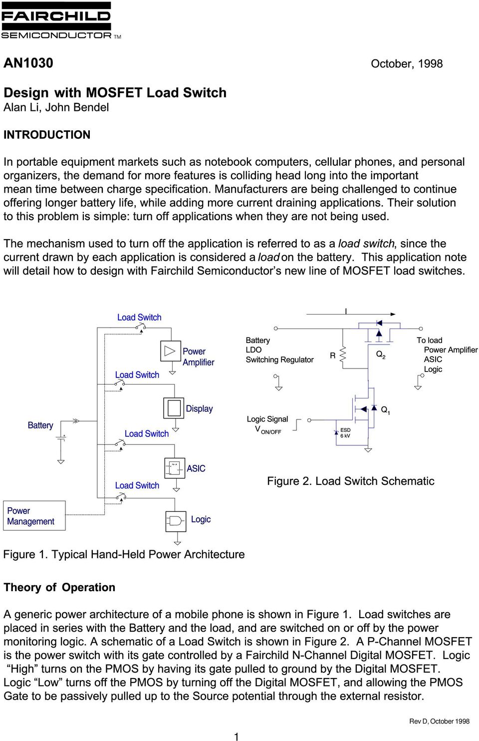
1 1 Rev D, October 1998
2 2

3 Ω Ω Ω Ω µ Ω Ω 3

4 = + = + = = + τ 4

5 Figure 4. Measured FDC6329L Dynamic Waveforms Figure 5. SPICE verification on FDC6329L Dynamic Waveforms Figure 6. SPICE result of FDC6329L V DROP vs I L 5

6 Appendix A Heat Flow Theory Applied to Power MOSFETs When a Power MOSFET operates with an appreciable current, its junction temperature is elevated. It is important to quantify its thermal limits in order to achieve acceptable performance and reliability. This limit is determined by summing the individual parts consisting of a series of temperature rises from the semiconductor junction to the operating environment. A one dimensional steady-state model of conduction heat transfer is demonstrated in figure 5. The heat generated at the device junction flows through the die to the die attach pad, through the lead frame to the surrounding case material, to the printed circuit board, and eventually to the ambient environment. There are also secondary heat paths. One is from the package to the ambient air. The other is from the drain lead frame to the detached source and gate leads then to the printed circuit board. These secondary heat paths are assumed to be negligible contributors to the heat flow in this analysis. RJA = RJC + RCA TJ-TA = PD * RJA Lead Frame Di e Junction Reference Case Reference for thermal couple in RJC measurement Sour ce, Gate Mounting Pad (Poor Thermal Path) MoldedPackage RJC RCA o T A = 25 C Via Boa rd Extended Copper Plane RJC(Component Variables) L eadframe Size & Material No. of Conduct ion Pins Die Si ze Die Attach Material Molding Compound Size & Material RC A(Applications Variables ) Drain Mounting Pad Mounting Pad Size, Mater ial, Shape & L ocation P lacement of M ounting Pad PCB Size & Material Amount of thermal Via Traces Length & Width Adjacent Heat Sources Air Flow Rate and Volume of Air Ambient Temperature...etc Figure 5: Cross-sectional view of a Power MOSFET mounted on a printed circuit board. Note that the case temperature is measured at the point where the drain lead(s) contact with the mounting pad surface. The increase of junction temperature above the surrounding environment is directly proportional to dissipated power and the thermal resistance. The steady-state junction-to-ambient thermal resistance, R JA, is defined as R JA = ( T J - T A ) / P where T J is the average temperature of the device junction. The term junction refers to the point of thermal reference of the semiconductor device. T A is the average temperature of the ambient environment. P is the power applied to the device which changes the junction temperature. R JA is a function of the junction-to-case R JC and case-to-ambient R CA thermal resistance R JA = R JC + R CA 6 Rev B, August 1998

7 where the case of a Power MOSFET is defined at the point of contact between the drain lead(s) and the mounting pad surface. R JC can be controlled and measured by the component manufacturer independent of the application and mounting method and is therefore the best means of comparing various suppliers component specifications for thermal performance. On the other hand, it is difficult to quantify R CA due to heavy dependence on the application. Before using the data sheet thermal data, the user should always be aware of the test conditions and justify the compatibility in the application. Appendix B Thermal Measurement Prior to any thermal measurement, a K factor must be determined. It is a linear factor related to the change of intrinsic diode voltage with respect to the change of junction temperature. From the slope of the curve shown in figure 6, K factor can be determined. It is approximately 2.2mV/ o C for most Power MOSFET devices NDS9956 V SD vs Temperature V GS = 0V V SD (V) mA = 2.39 mv/c 2mA = mA = mA = mA = 2.13 I SD = 20mA 10mA 5mA 2mA 1mA Temperature (C) Figure 6. K factors, slopes of a V SD vs temperature curves, of a typical Power MOSFET After the K factor calibration, the drain-source diode voltage of the device is measured prior to any heating. A pulse is then applied to the device and the drain-source diode voltage is measured 30us following the end of the power pulse. From the change of the drain-source diode voltage, the K factor, input power, and the reference temperature, the time dependent single pulsed junction-toreference thermal resistance can be calculated. From the single pulse curve on figure 7, duty cycle curves can be determined. Note: a curve set in which R JA is specified indicates that the part was characterized using the ambient as the thermal reference. The board layout specified in the data sheet notes will help determine the applicability of the curve set. 7

8 1 0.5 D = 0.5 r(t), NORMALIZED EFFECTIVE TRANSIENT THERMAL RESISTANCE Single Pulse R JA (t) = r(t) * R JA R JA = See Note 1a, b, c T J- T A = P * R JA (t) Duty Cycle, D = t 1 /t t 1, TIME (sec) P(pk) t 1 t 2 Figure 7. Normalized Transient Thermal Resistance Curves B.1 Junction-to-Ambient Thermal Resistance Measurement Equipment and Setup: Tesec DV240 Thermal Tester 1 cubic foot still air environment Thermal Test Board with 16 layouts defined by the size of the copper mounting pad and their relative surface placement. For layouts with copper on the top and bottom planes, there are 0.02 inch copper plated vias (heat pipes) connecting the two planes. See figure 2 and table 1 on the thermal application note for board layout and description. The conductivity of the FR-4 PCB used is 0.29 W/m-C. The length is 5.00 inches ± 0.005; width 4.50 inches ± 0.005; and thickness inches ± Oz copper clad PCB. The junction-to-ambient thermal measurement was conducted in accordance with the requirements of MIL-STD-883 and MIL-STD-750 with the exception of using 2 Oz copper and measuring diode current at 10mA. A test device is soldered on the thermal test board with minimum soldering. The copper mounting pad reaches the remote connection points through fine traces. Jumpers are used to bridge to the edge card connector. The fine traces and jumpers do not contribute significant thermal dissipation but serve the purpose of electrical connections. Using the intrinsic diode voltage measurement described above, the junction-to-ambient thermal resistance can be calculated. B.2 Junction-to-Case Thermal Resistance Measurement Equipment and Setup: Tesec DV240 Thermal Tester large aluminum heat sink type-k thermocouple with FLUKE 52 K/J Thermometer The drain lead(s) is soldered on a 0.5 x 1.5 x 0.05 copper plate. The plate is mechanically clamped to a heat sink which is large enough to be considered ideal. Thermal grease is applied in-between the two planes to provide good thermal contact. Theoretically the case temperature should be held constant regardless of the conditions. Thus a thermocouple is used and fixed at the point of contact between the drain lead(s) and the copper plate surface, to account for any heatsink temperature change. Using the intrinsic diode voltage measurement described earlier, the junction-to-case thermal resistance can be obtained. A plot of junction-to-case thermal resistance for 8
 connecting the two planes.")
9 various packages is shown in figure 8. Note R JC can vary with die size and the effect is more prominent as R JC decreases Junction-to-Case Thermal Resistance * Dual Leadframes ** Triple Leadframes rjcall.pre 10/4/95 Typical R jc ( C/W) o * 53.3 * SuperSOT-3 SuperSOT-6 Dual SO-8 Dual TSSOP SuperSOT-6 Single SO-8 Single SuperSOT-8 Single SOIC-16 TSOP-II SOT-223 D-PAK TO-263 ** 5 1 Figure 8. Junction-to-case thermal resistance R JC of various surface mount Power MOSFET packages. 9

10 References [1] K. Azar, S.S. Pan, J. Parry, H. Rosten, Effect of Circuit Board Parameters on Thermal Performance of Electronic Components in Natural Convection Cooling, IEEE 10th annual Semi-Therm Conference, Feb [2] A. Bar-Cohen, & A.D. Krauss, Advances in Thermal Modeling of Electronic Components & Systems, Vol 1, Hemisphere Publishing, Washington, D.C., [3] R.T. Bilson, M.R. Hepher, J.P. McCarthy, The Impact of Surface Mounted Chip Carrier Packaging on Thermal Management in Hybrid Microcircuit, Thermal Management Concepts in Microelectronics Packaging, InterFairchild Society for Hybrid Microelectronics, [4] R.A. Brewster, R.A. Sherif, Thermal Analysis of A Substrate with Power Dissipation in the Vias, IEEE 8th Annual Semi-Therm Conf., Austin, Tx, Feb [5] D. Edwards, Thermal Enhancement of IC Packages, IEEE 10th Annual Semi-Therm Conf., San Jose, Ca, Feb [6] S.S. Furkay, Convective Heat Transfer in Electronic Equipment: An Overview, Thermal Management Concepts, [7] C. Harper, Electronic Packaging & Interconnection Handbook, McGraw-Hill, NY, 1991, Ch. 2. [8] Y.M. Kasem, R.K. Williams, Thermal Design Principles and Characterization of Miniaturized Surface-Mount Packages for Power Electronics, IEEE 10th annual Semi-Therm Conf., San Jose, Ca, Feb [9] V. Manno, N.R. Kurita, K. Azar, Experimental Characterization of Board Conduction Effect, IEEE 9th Annual Semi- Therm Conf., [10] J.W. Sofia, Analysis of Thermal Transient Data with Synthesized Dynamic Models for Semiconductor Devices, IEEE 10th Annual Semi-Therm Conf., San Jose, Ca, Feb [11]G.R. Wagner, Circuit Board Material/Construction and its Effect on Thermal Management, Thermal Management Concepts, [12] M. Wills, Thermal Analysis of Air-Cooled Cbs, Electron Prod., pp , May [13] Motorola Application Note AN

11 TRADEMARKS The following are registered and unregistered trademarks Fairchild Semiconductor owns or is authorized to use and is not intended to be an exhaustive list of all such trademarks. ACEx CoolFET CROSSVOLT E 2 CMOS TM FACT FACT Quiet Series FAST FASTr GTO HiSeC ISOPLANAR MICROWIRE POP PowerTrench QS Quiet Series SuperSOT -3 SuperSOT -6 SuperSOT -8 TinyLogic DISCLAIMER FAIRCHILD SEMICONDUCTOR RESERVES THE RIGHT TO MAKE CHANGES WITHOUT FURTHER NOTICE TO ANY PRODUCTS HEREIN TO IMPROVE RELIABILITY, FUNCTION OR DESIGN. FAIRCHILD DOES NOT ASSUME ANY LIABILITY ARISING OUT OF THE APPLICATION OR USE OF ANY PRODUCT OR CIRCUIT DESCRIBED HEREIN; NEITHER DOES IT CONVEY ANY LICENSE UNDER ITS PATENT RIGHTS, NOR THE RIGHTS OF OTHERS. LIFE SUPPORT POLICY FAIRCHILD S PRODUCTS ARE NOT AUTHORIZED FOR USE AS CRITICAL COMPONENTS IN LIFE SUPPORT DEVICES OR SYSTEMS WITHOUT THE EXPRESS WRITTEN APPROVAL OF FAIRCHILD SEMICONDUCTOR CORPORATION. As used herein: 1. Life support devices or systems are devices or systems which, (a) are intended for surgical implant into the body, or (b) support or sustain life, or (c) whose failure to perform when properly used in accordance with instructions for use provided in the labeling, can be reasonably expected to result in significant injury to the user. PRODUCT STATUS DEFINITIONS Definition of Terms 2. A critical component is any component of a life support device or system whose failure to perform can be reasonably expected to cause the failure of the life support device or system, or to affect its safety or effectiveness. Datasheet Identification Product Status Definition Advance Information Preliminary No Identification Needed Formative or In Design First Production Full Production This datasheet contains the design specifications for product development. Specifications may change in any manner without notice. This datasheet contains preliminary data, and supplementary data will be published at a later date. Fairchild Semiconductor reserves the right to make changes at any time without notice in order to improve design. This datasheet contains final specifications. Fairchild Semiconductor reserves the right to make changes at any time without notice in order to improve design. Obsolete Not In Production This datasheet contains specifications on a product that has been discontinued by Fairchild semiconductor. The datasheet is printed for reference information only.

Maximum Power Enhancement Techniques for SO-8 Power MOSFETs
 AN1029 April, 1996 Maximum Power Enhancement Techniques for SO-8 Power MOSFETs 1. Introduction Alan Li, Brij Mohan, Steve Sapp, Izak Bencuya, Linh Hong As packages become smaller, achieving efficient thermal
Features 1.7 A, 20 V. R DS(ON) Symbol Parameter Ratings Units
 Symbol Parameter Ratings Units") N-Channel.5V Specified PowerTrench TM MOSFET April 999 General Description This N-Channel.5V specified MOSFET is produced using Fairchild Semiconductor's advanced PowerTrench process that has been especially
N-Channel.5V Specified PowerTrench TM MOSFET April 999 General Description This N-Channel.5V specified MOSFET is produced using Fairchild Semiconductor's advanced PowerTrench process that has been especially
Features. TA=25 o C unless otherwise noted
 NDSAN N-Channel, Logic Level, PowerTrench MOSFET June NDSAN General Description These N-Channel Logic Level MOSFETs are produced using Fairchild Semiconductor s advanced PowerTrench process that has been
Features S 1. TA=25 o C unless otherwise noted. (Note 1b) 0.8
 0.8") FC54P V P-Channel Logic Level PowerTrench MOSFET February 22 FC54P General escription This V P-Channel MOSFET uses Fairchild s high voltage PowerTrench process. It has been optimized for power management
FC54P V P-Channel Logic Level PowerTrench MOSFET February 22 FC54P General escription This V P-Channel MOSFET uses Fairchild s high voltage PowerTrench process. It has been optimized for power management
BUZ11. 30A, 50V, 0.040 Ohm, N-Channel Power MOSFET. Features. [ /Title (BUZ1 1) /Subject. (30A, 50V, 0.040 Ohm, N- Channel. Ordering Information
 /Subject. (30A, 50V, 0.040 Ohm, N- Channel. Ordering Information") Data Sheet June 1999 File Number 2253.2 [ /Title (BUZ1 1) /Subject (3A, 5V,.4 Ohm, N- Channel Power MOS- FET) /Autho r () /Keywords (Intersil Corporation, N- Channel Power MOS- FET, TO- 22AB ) /Creator
Data Sheet June 1999 File Number 2253.2 [ /Title (BUZ1 1) /Subject (3A, 5V,.4 Ohm, N- Channel Power MOS- FET) /Autho r () /Keywords (Intersil Corporation, N- Channel Power MOS- FET, TO- 22AB ) /Creator
QFET TM FQP50N06. Features. TO-220 FQP Series
 60V N-Channel MOSFET QFET TM General Description These N-Channel enhancement mode power field effect transistors are produced using Fairchild s proprietary, planar stripe, DMOS technology. This advanced
IRF510. 5.6A, 100V, 0.540 Ohm, N-Channel Power MOSFET. Features. Ordering Information. Symbol. Packaging. Data Sheet January 2002
 IRF5 Data Sheet January 22 5.6A, V,.5 Ohm, N-Channel Power MOSFET This N-Channel enhancement mode silicon gate power field effect transistor is an advanced power MOSFET designed, tested, and guaranteed
IRF840. 8A, 500V, 0.850 Ohm, N-Channel Power MOSFET. Features. Ordering Information. Symbol. Packaging. Data Sheet January 2002
 IRF84 Data Sheet January 22 8A, 5V,.85 Ohm, N-Channel Power MOSFET This N-Channel enhancement mode silicon gate power field effect transistor is an advanced power MOSFET designed, tested, and guaranteed
2N7000 / 2N7002 / NDS7002A N-Channel Enhancement Mode Field Effect Transistor
 November 995 N7 / N7 / NS7A N-Channel Enhancement Mode Field Effect Transistor General escription Features These N-Channel enhancement mode field effect transistors are produced using Fairchild's proprietary,
BDX33/A/B/C. Symbol Parameter Value Units V CBO Collector-Base Voltage : BDX33 : BDX33A : BDX33B : BDX33C
 Power Linear and Switching Applications High Gain General Purpose Power Darlington TR Complement to BDX34/34A/34B/34C respectively 1 TO-220 1.Base 2.Collector 3.Emitter NPN Epitaxial Silicon Transistor
IRF640, RF1S640, RF1S640SM
 IRF64, RFS64, RFS64SM Data Sheet January 22 8A, 2V,.8 Ohm, N-Channel Power MOSFETs These are N-Channel enhancement mode silicon gate power field effect transistors. They are advanced power MOSFETs designed,
BD434/436/438. Symbol Parameter Value Units V CBO Collector-Base Voltage : BD434 : BD436 : BD438
 Medium Power Linear and Switching Applications Complement to BD433, BD435 and BD437 respectively 1 TO26 1. Emitter 2.Collector 3.Base PNP Epitaxial Silicon Transistor Absolute Maximum Ratings T C =25 C
Si9953DY* Dual P-Channel Enhancement Mode MOSFET 9 '66 'UDLQ6RXUFHÃ9ROWDJH 9 9 *66 *DWH6RXUFHÃ9ROWDJH ± 9 Ã3XOVHG 3 '
 Si9953DY* Dual P-Channel Enhancement Mode MOSFET 0.250 Ω 0.400 Ω ÃÃÃÃÃÃÃ7 $ R &ÃXQOHVVÃRWKHUZLVHÃQRWHG 9 '66 'UDLQ6RXUFHÃ9ROWDJH 9 9 *66 *DWH6RXUFHÃ9ROWDJH ± 9, ' 'UDLQÃ&XUUHQW Ã&RQWLQXRXVÃ ÃÃÃÃÃÃÃÃÃÃÃÃÃÃÃÃÃÃÃÃÃÃ1RWHÃD
Description. TO-220F FDPF Series. Symbol Parameter FDP26N40 FDPF26N40 Units V DSS Drain to Source Voltage 400 V V GSS Gate to Source Voltage ±30 V
 FDP26N40 / FDPF26N40 N-Channel MOSFET 400V, 26A, 0.6Ω Features R DS(on) = 0.3Ω ( Typ.)@ V GS = 0V, I D = 3A Low gate charge ( Typ. 48nC) Low C rss ( Typ. 30pF) Fast switching 00% avalanche tested Improved
Advanced Monolithic Systems
 Advanced Monolithic Systems FEATURES Three Terminal Adjustable or Fixed oltages* 1.5, 1.8, 2.5, 2.85, 3.3 and 5. Output Current of 1A Operates Down to 1 Dropout Line Regulation:.2% Max. Load Regulation:.4%
TA = 25 C unless otherwise noted. Symbol Parameter Value Units
 Discrete POWER & Signal Technologies C B E TO-92 NPN Darlington Transistor This device is designed for applications requiring extremely high current gain at currents to 1.0 A. Sourced from Process 05.
P-Channel 20 V (D-S) MOSFET
 MOSFET") Si30CDS P-Channel 0 V (D-S) MOSFET MOSFET PRODUCT SUMMARY V DS (V) R DS(on) ( ) I D (A) a Q g (Typ.) - 0 0. at V GS = - 4.5 V - 3. 0.4 at V GS = -.5 V -.7 3.3 nc TO-36 (SOT-3) FEATURES Halogen-free According
Si30CDS P-Channel 0 V (D-S) MOSFET MOSFET PRODUCT SUMMARY V DS (V) R DS(on) ( ) I D (A) a Q g (Typ.) - 0 0. at V GS = - 4.5 V - 3. 0.4 at V GS = -.5 V -.7 3.3 nc TO-36 (SOT-3) FEATURES Halogen-free According
P-Channel 20-V (D-S) MOSFET
 MOSFET") Si33DS P-Channel -V (D-S) MOSFET PRODUCT SUMMARY V DS (V) R DS(on) (Ω) I D (A).39 at V GS = -.5 V -.7 -.5 at V GS = -.5 V -..68 at V GS = -.8 V - 3.5 FEATURES Halogen-free According to IEC 69-- Available
Si33DS P-Channel -V (D-S) MOSFET PRODUCT SUMMARY V DS (V) R DS(on) (Ω) I D (A).39 at V GS = -.5 V -.7 -.5 at V GS = -.5 V -..68 at V GS = -.8 V - 3.5 FEATURES Halogen-free According to IEC 69-- Available
NTMS4920NR2G. Power MOSFET 30 V, 17 A, N Channel, SO 8 Features
 NTMS9N Power MOSFET 3 V, 7 A, N Channel, SO Features Low R DS(on) to Minimize Conduction Losses Low Capacitance to Minimize Driver Losses Optimized Gate Charge to Minimize Switching Losses These Devices
N-Channel 100 V (D-S) MOSFET
 MOSFET") Si4DS N-Channel V (D-S) MOSFET MOSFET PRODUCT SUMMARY V DS (V) R DS(on) ( ) I D (A) a Q g (Typ.).4 at V GS = V..67 at V GS = 6 V..9 nc.78 at V GS = 4.5 V.7 FEATURES TrenchFET Power MOSFET % R g Tested
Si4DS N-Channel V (D-S) MOSFET MOSFET PRODUCT SUMMARY V DS (V) R DS(on) ( ) I D (A) a Q g (Typ.).4 at V GS = V..67 at V GS = 6 V..9 nc.78 at V GS = 4.5 V.7 FEATURES TrenchFET Power MOSFET % R g Tested
74VHC112 Dual J-K Flip-Flops with Preset and Clear
 74VHC112 Dual J-K Flip-Flops with Preset and Clear Features High speed: f MAX = 200MHz (Typ.) at V CC = 5.0V Low power dissipation: I CC = 2µA (Max.) at T A = 25 C High noise immunity: V NIH = V NIL =
FDS6679AZ P-Channel PowerTrench MOSFET -30V, -13A, 9mΩ General Description
 FS6679AZ P-Channel PowerTrench MOSFET -3V, -3A, 9mΩ General escription This P-Channel MOSFET is producted using Fairchild Semiconductor s advanced PowerTrench process that has been especially tailored
NUD4011. Low Current LED Driver
 NUD0 Low LED Driver This device is designed to replace discrete solutions for driving LEDs in AC/DC high voltage applications (up to 00 V). An external resistor allows the circuit designer to set the drive
CD4040BC, 12-Stage Ripple Carry Binary Counters CD4060BC, 14-Stage Ripple Carry Binary Counters
 CD4040BC, 12-Stage Ripple Carry Binary Counters CD4060BC, 14-Stage Ripple Carry Binary Counters Features Wide supply voltage range: 3.0V to 15V High noise immunity: 0.45 V DD (Typ.) Low power TTL compatibility:
CS8481. 3.3 V/250 ma, 5.0 V/100 ma Micropower Low Dropout Regulator with ENABLE
 3.3 /250 ma, 5.0 /100 ma Micropower Low Dropout Regulator with The CS8481 is a precision, dual Micropower linear voltage regulator. The switched 3.3 primary output ( OUT1 ) supplies up to 250 ma while
Applications. Pin 1 TOP. WL-CSP 0.8X0.8 Thin
 FDZ66PZ P-Channel.5 V Specified PowerTrench Thin WL-CSP MOSFET - V, -.6 A, 4 mω Features Max r DS(on) = 4 mω at V GS = -4.5 V, I D = - A Max r DS(on) = 8 mω at V GS = -.5 V, I D = -.5 A Max r DS(on) =
P-Channel 60 V (D-S) MOSFET
 MOSFET") TP6K P-Channel 6 V (D-S) MOSFET G S PRODUCT SUMMARY V DS (V) R DS(on) ( ) V GS(th) (V) I D (ma) - 6 6 at V GS = - V - to - - 85 TO-6 (SOT-) Top View D Marking Code: 6Kwll 6K = Part Number Code for TP6K
TP6K P-Channel 6 V (D-S) MOSFET G S PRODUCT SUMMARY V DS (V) R DS(on) ( ) V GS(th) (V) I D (ma) - 6 6 at V GS = - V - to - - 85 TO-6 (SOT-) Top View D Marking Code: 6Kwll 6K = Part Number Code for TP6K
FSAL200 Wide Bandwidth Quad 2:1 Analog Multiplexer / De-multiplexer Switch
 FSAL200 Wide Bandwidth Quad 2:1 Analog Multiplexer / De-multiplexer Switch Features Typical 6Ω Switch Connection Between Two Ports Minimal Propagation Delay Through the Switch Low I CC Zero Bounce in Flow-Through
LM1117/LM1117I 800mA Low-Dropout Linear Regulator
 LM1117/LM1117I 800mA Low-Dropout Linear Regulator General Description The LM1117 is a series of low dropout voltage regulators with a dropout of 1.2 at 800mA of load current. It has the same pin-out as
1N5820, 1N5821, 1N5822. Axial Lead Rectifiers SCHOTTKY BARRIER RECTIFIERS 3.0 AMPERES 20, 30, 40 VOLTS
 1N58, 1N5821, 1N5822 1N58 and 1N5822 are Preferred Devices Rectifiers This series employs the Schottky Barrier principle in a large area metal-to-silicon power diode. State-of-the-art geometry features
LM3940 1A Low Dropout Regulator for 5V to 3.3V Conversion
 1A Low Dropout Regulator for 5V to 3.3V Conversion General Description The LM3940 is a 1A low dropout regulator designed to provide 3.3V from a 5V supply. The LM3940 is ideally suited for systems which
Automotive P-Channel 60 V (D-S) 175 C MOSFET
 175 C MOSFET") Automotive P-Channel 6 V (D-S) 75 C MOSFET SQ36AEES PRODUCT SUMMARY V DS (V) -6 R DS(on) () at V GS = - V 7 R DS(on) () at V GS = -4.5 V.3 I D (A) -.9 Configuration Single D 3 SOT-3 (TO-36) G Top View
Automotive P-Channel 6 V (D-S) 75 C MOSFET SQ36AEES PRODUCT SUMMARY V DS (V) -6 R DS(on) () at V GS = - V 7 R DS(on) () at V GS = -4.5 V.3 I D (A) -.9 Configuration Single D 3 SOT-3 (TO-36) G Top View
Load Switch with Level-Shift
 Load Switch with Level-Shift PRODUCT SUMMARY V IN (V DS2 ) (V) R DS(on) (Ω) I D (A).5 to 2 DESCRIPTION.54 at V IN = 4.5 V 3.9.77 at V IN = 2.5 V 3.2.6 at V IN =.8 V 2.8.65 at V IN =.5 V 2.2 The includes
TSM2N7002K 60V N-Channel MOSFET
 SOT-23 SOT-323 Pin Definition: 1. Gate 2. Source 3. Drain PRODUCT SUMMARY V DS (V) R DS(on) (Ω) I D (ma) 5 @ V GS = 10V 100 60 5.5 @ V GS = 5V 100 Features Low On-Resistance ESD Protection High Speed Switching
AP331A XX G - 7. Lead Free G : Green. Packaging (Note 2)
") Features General Description Wide supply Voltage range: 2.0V to 36V Single or dual supplies: ±1.0V to ±18V Very low supply current drain (0.4mA) independent of supply voltage Low input biasing current:
Features General Description Wide supply Voltage range: 2.0V to 36V Single or dual supplies: ±1.0V to ±18V Very low supply current drain (0.4mA) independent of supply voltage Low input biasing current:
C106 Series. Sensitive Gate Silicon Controlled Rectifiers
 C6 Series Sensitive Gate Silicon Controlled Rectifiers Reverse Blocking Thyristors Glassivated PNPN devices designed for high volume consumer applications such as temperature, light, and speed control;
NUD4001, NSVD4001. High Current LED Driver
 NUD, NSVD High Current LED Driver This device is designed to replace discrete solutions for driving LEDs in low voltage AC DC applications. V, V or V. An external resistor allows the circuit designer to
MBR20200CT Dual High Voltage Schottky Rectifier
 MBR20200CT Dual High Voltage Schottky Rectifier Features Low Forward Voltage Drop Low Power Loss and High Efficiency High Surge Capability RoHS Compliant Matte Tin (Sn) Lead Finish Terminal Leads Surface
LM79XX Series 3-Terminal Negative Regulators
 LM79XX Series 3-Terminal Negative Regulators General Description The LM79XX series of 3-terminal regulators is available with fixed output voltages of b5v b8v b12v and b15v These devices need only one
P-Channel 12 V (D-S) MOSFET
 MOSFET") New Product SiEH P-Channel V (-S) MOSFET PROUCT SUMMARY V S (V) R S(on) ( ) I (A) a Q g (Typ.) G -. at V GS = -.5 V -.6 at V GS = -.5 V -.7 at V GS = -.8 V -. at V GS = -.5 V - SOT-6 SC-7 (6-LEAS) Top
New Product SiEH P-Channel V (-S) MOSFET PROUCT SUMMARY V S (V) R S(on) ( ) I (A) a Q g (Typ.) G -. at V GS = -.5 V -.6 at V GS = -.5 V -.7 at V GS = -.8 V -. at V GS = -.5 V - SOT-6 SC-7 (6-LEAS) Top
CAT4101TV. 1 A Constant-Current LED Driver with PWM Dimming
 A Constant-Current LED Driver with PWM Dimming Description The CAT4 is a constant current sink driving a string of high brightness LEDs up to A with very low dropout of.5 V at full load. It requires no
MC33064DM 5 UNDERVOLTAGE SENSING CIRCUIT
 Order this document by MC3464/D The MC3464 is an undervoltage sensing circuit specifically designed for use as a reset controller in microprocessor-based systems. It offers the designer an economical solution
Power MOSFET. IRF510PbF SiHF510-E3 IRF510 SiHF510. PARAMETER SYMBOL LIMIT UNIT Drain-Source Voltage V DS 100 V Gate-Source Voltage V GS ± 20
 Power MOSFET PRODUCT SUMMARY (V) 100 R DS(on) () = 0.54 Q g max. (nc) 8.3 Q gs (nc) 2.3 Q gd (nc) 3.8 Configuration Single D TO220AB G FEATURES Dynamic dv/dt rating Available Repetitive avalanche rated
PDS5100H. Product Summary. Features and Benefits. Mechanical Data. Description and Applications. Ordering Information (Note 5) Marking Information
 Marking Information") Green 5A HIGH VOLTAGE SCHOTTKY BARRIER RECTIFIER POWERDI 5 Product Summary I F V R V F MAX (V) I R MAX (ma) (V) (A) @ +25 C @ +25 C 1 5..71.35 Description and Applications This Schottky Barrier Rectifier
Green 5A HIGH VOLTAGE SCHOTTKY BARRIER RECTIFIER POWERDI 5 Product Summary I F V R V F MAX (V) I R MAX (ma) (V) (A) @ +25 C @ +25 C 1 5..71.35 Description and Applications This Schottky Barrier Rectifier
CHAPTER 6 THERMAL DESIGN CONSIDERATIONS. page. Introduction 6-2. Thermal resistance 6-2. Junction temperature 6-2. Factors affecting R th(j-a) 6-2
 6-2") CHAPTER 6 THERMAL DESIGN CONSIDERATIONS page Introduction 6-2 Thermal resistance 6-2 Junction temperature 6-2 Factors affecting 6-2 Thermal resistance test methods 6-3 Test procedure 6-3 Forced air factors
CHAPTER 6 THERMAL DESIGN CONSIDERATIONS page Introduction 6-2 Thermal resistance 6-2 Junction temperature 6-2 Factors affecting 6-2 Thermal resistance test methods 6-3 Test procedure 6-3 Forced air factors
Power MOSFET FEATURES. IRF610PbF SiHF610-E3 IRF610 SiHF610. PARAMETER SYMBOL LIMIT UNIT Drain-Source Voltage V DS 200 V Gate-Source Voltage V GS ± 20
 Power MOSFET PRODUCT SUMMARY (V) 00 R DS(on) ( ) = 1.5 Q g (Max.) (nc) 8. Q gs (nc) 1.8 Q gd (nc) 4.5 Configuration Single FEATURES Dynamic dv/dt Rating Repetitive Avalanche Rated Fast Switching Ease of
T A = 25 C (Notes 3 & 5) Product Marking Reel size (inches) Tape width (mm) Quantity per reel DMC4040SSD-13 C4040SD 13 12 2,500
 Product Marking Reel size (inches) Tape width (mm) Quantity per reel DMC4040SSD-13 C4040SD 13 12 2,500") Product Line of 4 COMPLEMENTRY PIR ENHNCEMENT MODE MOSFET Product Summary Device (BR)DSS R DS(on) max I D max () T = 25 C (Notes 3 & 5) 25mΩ @ = 1 7.5 Q1 4 4mΩ @ = 4.5 6.2 Features and Benefits Matched
Product Line of 4 COMPLEMENTRY PIR ENHNCEMENT MODE MOSFET Product Summary Device (BR)DSS R DS(on) max I D max () T = 25 C (Notes 3 & 5) 25mΩ @ = 1 7.5 Q1 4 4mΩ @ = 4.5 6.2 Features and Benefits Matched
1.5A Ultra Low Dropout Linear Regulator TJ3965
 FEATURES Ultra Low Dropout Voltage Low Ground Pin Current Excellent Line and Load Regulation Guaranteed Output Current of 1.5A Available in MSOP8, SOP8, SOP8PP, SOT223, TO252, TO263, TO220, and SOT89 Packages
Power MOSFET FEATURES. IRFZ44PbF SiHFZ44-E3 IRFZ44 SiHFZ44 T C = 25 C
 Power MOSFET PRODUCT SUMMARY (V) 60 R DS(on) (Ω) V GS = 10 V 0.028 Q g (Max.) (nc) 67 Q gs (nc) 18 Q gd (nc) 25 Configuration Single FEATURES Dynamic dv/dt Rating 175 C Operating Temperature Fast Switching
Dual P-Channel 2.5 V (G-S) MOSFET
 MOSFET") Si593DC Dual P-Channel.5 V (G-S) MOSFET PRODUCT SUMMARY V DS (V) R DS(on) (Ω) I D (A).55 at V GS = -.5 V ±.9 -.8 at V GS = - 3.6 V ±.7.6 at V GS = -.5 V ±. FEATURES Halogen-free According to IEC 69-- Definition
Si593DC Dual P-Channel.5 V (G-S) MOSFET PRODUCT SUMMARY V DS (V) R DS(on) (Ω) I D (A).55 at V GS = -.5 V ±.9 -.8 at V GS = - 3.6 V ±.7.6 at V GS = -.5 V ±. FEATURES Halogen-free According to IEC 69-- Definition
Power MOSFET FEATURES. IRF740PbF SiHF740-E3 IRF740 SiHF740. PARAMETER SYMBOL LIMIT UNIT Drain-Source Voltage V DS 400 V Gate-Source Voltage V GS ± 20
 Power MOSFET PRODUCT SUMMARY (V) 400 R DS(on) (Ω) = 0.55 Q g (Max.) (nc) 63 Q gs (nc) 9.0 Q gd (nc) 3 Configuration Single FEATURES Dynamic dv/dt Rating Repetitive Avalanche Rated Fast Switching Ease of
SDC15. TVS Diode Array for ESD Protection of 12V Data and Power Lines. PROTECTION PRODUCTS Description. Features. Mechanical Characteristics
 Description The SDC15 transient voltage suppressor (TVS) is designed to protect components which are connected to data and transmission lines from voltage surges caused by electrostatic discharge (ESD),
NSI45060JDT4G. Adjustable Constant Current Regulator & LED Driver. 45 V, 60 100 ma 15%, 2.7 W Package
 NSI5JDTG Adjustable Constant Current Regulator & Driver 5 V, ma 5%, 2.7 W Package The adjustable constant current regulator (CCR) is a simple, economical and robust device designed to provide a cost effective
LM2941/LM2941C 1A Low Dropout Adjustable Regulator
 LM2941/LM2941C 1A Low Dropout Adjustable Regulator General Description The LM2941 positive voltage regulator features the ability to source 1A of output current with a typical dropout voltage of 0.5V and
MC14001B Series. B Suffix Series CMOS Gates MC14001B, MC14011B, MC14023B, MC14025B, MC14071B, MC14073B, MC14081B, MC14082B
 MC4B Series BSuffix Series CMOS Gates MC4B, MC4B, MC4B, MC4B, MC4B, MC4B, MC4B, MC4B The B Series logic gates are constructed with P and N channel enhancement mode devices in a single monolithic structure
Power MOSFET FEATURES. IRL540PbF SiHL540-E3 IRL540 SiHL540
 Power MOSFET PRODUCT SUMMARY (V) 100 R DS(on) (Ω) = 5.0 V 0.077 Q g (Max.) (nc) 64 Q gs (nc) 9.4 Q gd (nc) 27 Configuration Single TO220AB G DS ORDERING INFORMATION Package Lead (Pb)free SnPb G D S NChannel
AN1703 APPLICATION NOTE GUIDELINES FOR USING ST S MOSFET SMD PACKAGES
 AN170 APPLICATION NOTE GUIELINES FO USING ST S MOSFET SM PACKAGES 1. ABSTACT.Gulino The trend from through-hole packages to low-cost SM-applications is marked by the improvement of chip technologies. "Silicon
N-channel enhancement mode TrenchMOS transistor
 FEATURES SYMBOL QUICK REFERENCE DATA Trench technology d V DSS = V Low on-state resistance Fast switching I D = A High thermal cycling performance Low thermal resistance R DS(ON) mω (V GS = V) g s R DS(ON)
CS4525 Power Calculator
 1. OVERVIEW CS4525 Power Calculator The CS4525 Power Calculator provides many important application-specific performance numbers for the CS4525 based on user-supplied design parameters. The Power Calculator
Application Note AN-0994 Maximizing the Effectiveness of your SMD Assemblies
 Application Note AN-0994 Maximizing the Effectiveness of your SMD Assemblies Table of Contents Page Method...2 Thermal characteristics of SMDs...2 Adhesives...4 Solder pastes...4 Reflow profiles...4 Rework...6
LM1084 5A Low Dropout Positive Regulators
 5A Low Dropout Positive Regulators General Description The LM1084 is a series of low dropout voltage positive regulators with a maximum dropout of 1.5 at 5A of load current. It has the same pin-out as
SURFACE MOUNT LED LAMP STANDARD BRIGHT 0606
 PACKAGE DIMENSIONS 0.075 (1.9) 0.063 (1.6) 0.035 (0.9) TOP 0.047 (1.2) 0.012 (0.3) 0.032 [0.8] SIDE 0.043 [1.1] 1 3 0.020 [0.5] 2 4 BOTTOM CATHODE MASK 1 2 3 4 HER / AlGaAs Red / Yellow (for-34) Green
1-Mbit (128K x 8) Static RAM
 Static RAM") 1-Mbit (128K x 8) Static RAM Features Pin- and function-compatible with CY7C109B/CY7C1009B High speed t AA = 10 ns Low active power I CC = 80 ma @ 10 ns Low CMOS standby power I SB2 = 3 ma 2.0V Data Retention
1-Mbit (128K x 8) Static RAM Features Pin- and function-compatible with CY7C109B/CY7C1009B High speed t AA = 10 ns Low active power I CC = 80 ma @ 10 ns Low CMOS standby power I SB2 = 3 ma 2.0V Data Retention
TYPICAL APPLICATION CIRCUIT. ORDER INFORMATION SOP-EP 8 pin A703EFT (Lead Free) A703EGT (Green)
 A703EGT (Green)") www.addmtek.com 2 CHANNELS 150mA HIGH VOLTAGE ADJUSTABLE CURRENT REGULATOR DESCRIPTION A703 is a high voltage, adjustable constant current driver for LED applications. Two regulated current ports are designed
www.addmtek.com 2 CHANNELS 150mA HIGH VOLTAGE ADJUSTABLE CURRENT REGULATOR DESCRIPTION A703 is a high voltage, adjustable constant current driver for LED applications. Two regulated current ports are designed
CAN bus ESD protection diode
 Rev. 04 15 February 2008 Product data sheet 1. Product profile 1.1 General description in a small SOT23 (TO-236AB) Surface-Mounted Device (SMD) plastic package designed to protect two automotive Controller
BSP52T1 MEDIUM POWER NPN SILICON SURFACE MOUNT DARLINGTON TRANSISTOR
 Preferred Device This NPN small signal darlington transistor is designed for use in switching applications, such as print hammer, relay, solenoid and lamp drivers. The device is housed in the SOT-223 package,
C Soldering Temperature, for 10 seconds 300 (1.6mm from case )
") l Advanced Process Technology l Ultra Low On-Resistance l Dynamic dv/dt Rating l 75 C Operating Temperature l Fast Switching l Fully Avalanche Rated l Optimized for SMPS Applications Description Advanced
l Advanced Process Technology l Ultra Low On-Resistance l Dynamic dv/dt Rating l 75 C Operating Temperature l Fast Switching l Fully Avalanche Rated l Optimized for SMPS Applications Description Advanced
Power MOSFET FEATURES. IRF740PbF SiHF740-E3 IRF740 SiHF740. PARAMETER SYMBOL LIMIT UNIT Drain-Source Voltage V DS 400 V Gate-Source Voltage V GS ± 20
 Power MOSFET PRODUCT SUMMARY (V) 400 R DS(on) (Ω) = 0.55 Q g (Max.) (nc) 63 Q gs (nc) 9.0 Q gd (nc) 3 Configuration Single FEATURES Dynamic dv/dt Rating Repetitive Avalanche Rated Fast Switching Ease of
N-Channel 30-V (D-S) MOSFET
 MOSFET") Si3456V N-Channel 3-V (-S) MOSFET PROUCT SUMMARY V S (V) R S(on) (Ω) I (A) d Q g (Typ.) 3.4 at V GS = V 6.3.5 at V GS = 4.5 V 5.7 TSOP-6 Top View.8 nc FEATURES Halogen-free According to IEC 649-- efinition
Si3456V N-Channel 3-V (-S) MOSFET PROUCT SUMMARY V S (V) R S(on) (Ω) I (A) d Q g (Typ.) 3.4 at V GS = V 6.3.5 at V GS = 4.5 V 5.7 TSOP-6 Top View.8 nc FEATURES Halogen-free According to IEC 649-- efinition
Last Time Buy. Deadline for receipt of LAST TIME BUY orders: April 30, 2011
 Last Time Buy This part is in production but has been determined to be LAST TIME BUY. This classification indicates that the product is obsolete and notice has been given. Sale of this device is currently
N-Channel 20-V (D-S) 175 C MOSFET
 175 C MOSFET") N-Channel -V (D-S) 75 C MOSFET SUD7N-4P PRODUCT SUMMARY V DS (V) r DS(on) ( ) (A) a.37 @ V GS = V 37.6 @ V GS = 4.5 V 9 TO-5 D FEATURES TrenchFET Power MOSFET 75 C Junction Temperature PWM Optimized for
N-Channel -V (D-S) 75 C MOSFET SUD7N-4P PRODUCT SUMMARY V DS (V) r DS(on) ( ) (A) a.37 @ V GS = V 37.6 @ V GS = 4.5 V 9 TO-5 D FEATURES TrenchFET Power MOSFET 75 C Junction Temperature PWM Optimized for
Power MOSFET FEATURES. IRF540PbF SiHF540-E3 IRF540 SiHF540. PARAMETER SYMBOL LIMIT UNIT Drain-Source Voltage V DS 100 V Gate-Source Voltage V GS ± 20
 Power MOSFET PRODUCT SUMMARY (V) 100 R DS(on) ( ) = 0.077 Q g (Max.) (nc) 72 Q gs (nc) 11 Q gd (nc) 32 Configuration Single TO220AB G DS ORDERING INFORMATION Package Lead (Pb)free SnPb G D S NChannel MOSFET
Current Limiting Power Resistors for High-Power LED Module Lighting Applications
 Current Limiting Power Resistors for High-Power LED Module Lighting Applications PWR263 An ongoing trend toward miniaturization of virtually all electronics is accompanied by the demand for a reduction
Automotive MOSFETs in Linear Applications: Thermal Instability
 Application Note, V1.0, May 2005 Automotive MOSFETs in Linear Applications: Thermal Instability by Peter H. Wilson Automotive Power N e v e r s t o p t h i n k i n g. - 1 - Table of Content 1. Introduction...
Power MOSFET FEATURES. IRF9640PbF SiHF9640-E3 IRF9640 SiHF9640
 Power MOSFET PRODUCT SUMMARY V DS (V) 200 R DS(on) (Ω) = 10 V 0.50 Q g (Max.) (nc) 44 Q gs (nc) 7.1 Q gd (nc) 27 Configuration Single TO220AB G DS ORDERING INFORMATION Package Lead (Pb)free SnPb G S D
A I DM. W/ C V GS Gate-to-Source Voltage ± 20. Thermal Resistance Symbol Parameter Typ. Max. Units
 V DS 2 V V GS Max ± 2 V R DSon) max @V GS = V) 24 m * PD - 9787A HEXFET Power MOSFET R DSon) max @V GS = 4.V) 4 m 6 Micro3 TM SOT-23) Applications) Load System Switch Features and Benefits Features Benefits
A I DM. W/ C V GS Gate-to-Source Voltage ± 12. Thermal Resistance Symbol Parameter Typ. Max. Units
 V DS 2 V V GS Max ±2 V * PD - 973A HEXFET Power MOSFET R DSon) max @V GS = 4.V) 2. m R DSon) max @V GS = 2.V) 27. m 6 Micro3 TM SOT-23) Applications) Load System Switch Features and Benefits Features Benefits
LM380 Audio Power Amplifier
 LM380 Audio Power Amplifier General Description The LM380 is a power audio amplifier for consumer application. In order to hold system cost to a minimum, gain is internally fixed at 34 db. A unique input
10 ma LED driver in SOT457
 SOT457 in SOT457 Rev. 1 20 February 2014 Product data sheet 1. Product profile 1.1 General description LED driver consisting of resistor-equipped PNP transistor with two diodes on one chip in an SOT457
INTEGRATED CIRCUITS. 74LVC08A Quad 2-input AND gate. Product specification IC24 Data Handbook. 1997 Jun 30
 INTEGRATED CIRCUITS IC24 Data Handbook 1997 Jun 30 FEATURES Wide supply voltage range of 1.2 V to 3.6 V In accordance with JEDEC standard no. 8-1A Inputs accept voltages up to 5.5 V CMOS low power consumption
IRLR8743PbF IRLU8743PbF HEXFET Power MOSFET
 Applications l High Frequency Synchronous Buck Converters for Computer Processor Power l High Frequency Isolated DC-DC Converters with Synchronous Rectification for Telecom and Industrial Use l Lead-Free
BSN20. 1. Description. 2. Features. 3. Applications. 4. Pinning information. N-channel enhancement mode field-effect transistor
 Rev. 3 26 June 2 Product specification. Description in a plastic package using TrenchMOS technology. Product availability: in SOT23. 2. Features TrenchMOS technology Very fast switching Logic level compatible
LM380 Audio Power Amplifier
 LM380 Audio Power Amplifier General Description The LM380 is a power audio amplifier for consumer application In order to hold system cost to a minimum gain is internally fixed at 34 db A unique input
How to Read a Datasheet
 How to Read a Datasheet Prepared for the WIMS outreach program 5/6/02, D. Grover In order to use a PIC microcontroller, a flip-flop, a photodetector, or practically any electronic device, you need to consult
Application Note, V1.0, 2008 AN2008-03. Thermal equivalent circuit models. replaces AN2001-05. Industrial Power
 Application Note, V1.0, 2008 AN2008-03 Thermal equivalent circuit models replaces AN2001-05 Industrial Power Edition 2008-06-16 Published by Infineon Technologies AG 59568 Warstein, Germany Infineon Technologies
N-Channel 60-V (D-S), 175 C MOSFET
, 175 C MOSFET") N-Channel 6-V (D-S), 75 C MOSFET SUP/SUB7N6-4 V (BR)DSS (V) r DS(on) ( ) (A) 6.4 7 a TO-22AB D TO-263 DRAIN connected to TAB G G D S Top View SUP7N6-4 G D S Top View SUB7N6-4 S N-Channel MOSFET Parameter
N-Channel 6-V (D-S), 75 C MOSFET SUP/SUB7N6-4 V (BR)DSS (V) r DS(on) ( ) (A) 6.4 7 a TO-22AB D TO-263 DRAIN connected to TAB G G D S Top View SUP7N6-4 G D S Top View SUB7N6-4 S N-Channel MOSFET Parameter
1N5401-1N5408 General-Purpose Rectifiers
 N540 - N5408 General-Purpose Rectifiers Features 3.0 A Operation at T A = 75 C with No Thermal Runaway High Current Capability Low Leakage DO-20AD COLOR BAND DENOTES CATHODE August 205 N540 - N5408 General-Purpose
LM2941 LM2941C 1A Low Dropout Adjustable Regulator
 June 1994 LM2941 LM2941C 1A Low Dropout Adjustable Regulator General Description The LM2941 positive voltage regulator features the ability to source 1A of output current with a typical dropout voltage
TSM020N03PQ56 30V N-Channel MOSFET
 PDFN56 Pin Definition: 1. Source 8. Drain 2. Source 7. Drain 3. Source 6. Drain 4. Gate 5. Drain Key Parameter Performance Parameter Value Unit V DS 30 V R DS(on) (max) V GS = 10V 2 V GS = 4.5V 3 mω Q
TIP140, TIP141, TIP142, (NPN); TIP145, TIP146, TIP147, (PNP) Darlington Complementary Silicon Power Transistors
; TIP145, TIP146, TIP147, (PNP) Darlington Complementary Silicon Power Transistors") TIP140, TIP141, TIP142, (); TIP145, TIP146, TIP147, () Darlington Complementary Silicon Power Transistors Designed for generalpurpose amplifier and low frequency switching applications. Features High DC
TIP140, TIP141, TIP142, (); TIP145, TIP146, TIP147, () Darlington Complementary Silicon Power Transistors Designed for generalpurpose amplifier and low frequency switching applications. Features High DC
AP1509. 150KHz, 2A PWM BUCK DC/DC CONVERTER. Description. Pin Assignments V IN. Applications. Features. (Top View) GND GND. Output AP1509 GND GND
 GND GND. Output AP1509 GND GND") Description Pin Assignments The series are monolithic IC designed for a stepdown DC/DC converter, and own the ability of driving a 2A load without additional transistor. It saves board space. The external
Description Pin Assignments The series are monolithic IC designed for a stepdown DC/DC converter, and own the ability of driving a 2A load without additional transistor. It saves board space. The external