Testing of Digital System-on- Chip (SoC)
|
|
|
- Caitlin O’Neal’
- 10 years ago
- Views:
Transcription
1 Testing of Digital System-on- Chip (SoC) 1
")
2 Outline of the Talk Introduction to system-on-chip (SoC) design Approaches to SoC design SoC test requirements and challenges Core test wrapper P1500 core test standard Summary 2

3 What is a System-on-Chip (SoC)? The integration of a complete system on an IC chip. Earlier consisted of multiple IC chips. May include multiple types of design blocks and intellectual property (IP). Digital logic blocks, processors, memories and analog circuitry. Typically SoC s are designed using embedded reusable cores. 3
.")
4 Traditional vs. SoC Design Traditional IC design Design the whole IC from scratch. Reuse: standard cell library, memory, etc. SoC (core-based) design Reuse: large modules, like CPU, DSP, MPEG, I/O controllers, analog modules, etc. Reduced time to market. Sharing / importing expertise. 4
 design Reuse: large modules, like CPU, DSP, MPEG, I/O")
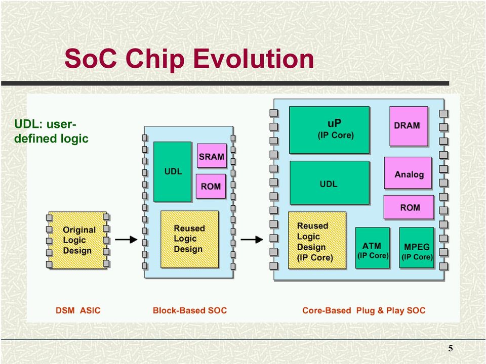
5 SoC Chip Evolution UDL: userdefined logic 5
6 PCB/SoB vs. SoC PCB/SoB Tested parts In-circuit test (ICT) Easy test access Bulky Slow High assembly cost SoC High reliability Fast interconnects Low cost Untested cores No internal test access Mixed-signal devices 6

7 SoB vs. SoC Test Process 7
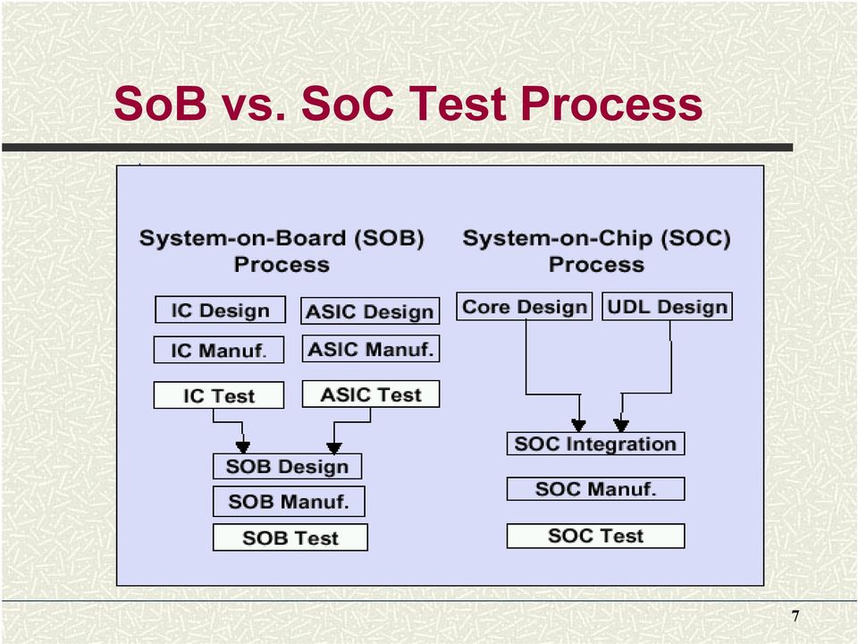
8 SoB vs. SoC Test Process (contd.) SoC realization process is analogous to SoB using standard parts. SoC cores and UDL not manufactured and tested individually. Cores and UDL are tested together. SoC test integration requires test data provided with each core. core test integration methodology and tools. 8

9 Core-based Design Cores are pre-designed, verified but untested functional blocks. Soft core synthesizable RTL Firm core gate-level netlist Hard core non-modifiable layout (legacy core) Core is the intellectual property of vendor. Internal details not available to user. Core-vendor supplied tests must be applied to embedded cores. 9

10 Core Types A soft core is a technology-independent synthesizable RTL circuit description. Specified in a high-level description language, and hence technology independent. Layout is completely flexible. Performance and area depend on cell library used. Synthesis, test, timing analysis, and verification are required. A firm core is a technology-dependent gate-level netlist that meets timing constraints. Layout is flexible. Performance and area are more predictable. May be encrypted to protect IP. 10

11 Contd. A hard core includes layout and timing information. Given as layout files that cannot be modified. Highly optimized for area and performance, and synthesized to a specific technology. Includes behavioral model for simulation. May be encrypted. Test sets (test stimuli and test responses) are given. Gives less flexibility to the core integrator, but saves design time and effort. 11

12 SoC Test Requirements Deeply embedded cores Need Test Access Mechanism to access the input/output pins of the core being tested. External ATE inefficiency Need on- chip ATE. Mixing technologies: logic, processor, memory, analog components Need various DFT/ BIST techniques. 12

13 SoC Test Requirements (contd.) Multiple hardware description level for cores Need to insert DFT/ BIST at various levels. Different core providers and SoC test developers Need standard for test integration. Core/ test reuse Need plug-and-play test mechanism. IP protection Need core test standard/ document. 13

14 SoC Test Methodology Study functions and architectures in each module of a general SoC. Design each module. Apply proper testing methods to each module. Add wrapper to each core (module). Integrate the IP testing using some standard. P-1500 core test standard. 14
.")
15 Test Challenges in SoC Design For conventional ASIC s and standard IC s mounted on a circuit board: The individual chips are tested separately before being assembled on the board. With SoC design, The individual cores are not tested before the complete SoC is fabricated. 15

16 Test Challenges in SoC Design (contd.) There is no direct access to the core I/O ports from the chip I/O s. Often involves an additional DFT effort. Core integration Use of multiple cores within one design. Cores may use different DFT strategies and test methods. Compose an integrated test and its control mechanism for the overall system chip. Requires scheduling to meet chip-level requirements. 16

17 Test-Wrapper for a Core Test-wrapper (or collar) Logic added around a core. Provides test access to the embedded core. Source TAM Core under test TAM Sink Wrapper 17

18 Contd. Test-wrapper provides: For each core input terminal: A normal mode: Core terminal driven by host chip. An external test mode: Wrapper element observes core input terminal for interconnect test. An internal test mode: Wrapper element controls state of core input terminal for testing the logic inside core. 18

19 Contd. For each core output terminal: A normal mode: Host chip driven by core terminal. An external test mode: Host chip is driven by wrapper element for interconnect test. An internal test mode: Wrapper element observes core outputs for core test. 19

20 A Test-Wrapper (similar to P1500) Wrapper elements Functional core inputs Core Functional core outputs from/to External Test pins (TAM) Instr. Reg. to/from TAP Wrapper test controller 20
 Instr. Reg.")
21 DFT Architecture for SoC Test source Functional inputs User defined test access mechanism (TAM) Test Module 1 wrapper Func. outputs Func. inputs Test Module N wrapper Test sink Functional outputs Instruction register control Serial instruction data Test access port (TAP) SOC inputs TDI TCK TMS TRST TDO SOC outputs 21
22 SoC DFT Components 1. Test source: Provides test vectors via on-chip LFSR, counter, ROM, or off-chip ATE. 2. Test sink: Provides output verification using on-chip signature analyzer, or off-chip ATE. 22
23 Contd. 3. Test access mechanism (TAM): User-defined test data communication structure. Carries test signals from source to module, and module to sink. Tests module interconnects via test-wrappers. May contain bus, boundary-scan and analog test bus components. 23
24 Contd. 4. Test controller: Boundary-scan test access port (TAP). Receives control signals from outside. Serially loads test instructions in test-wrappers. 24
25 IEEE P1500 Organization Aim is to standardize interface between core provider and core user. P1500 specifies: 1. Standardized, scalable core test wrapper. 2. Core test information model. Described in core test language (CTL). 3. Two compliance levels. IEEE 1500 unwrapped. IEEE 1500 wrapped. 25
26 IEEE P1500 Core Test Standard Goals Define test interface between core and SoC. Core isolation. Plug-and-play protocols. Scope Standardize core isolation protocols and test modes. Does not address test access mechanism (TAM) design. Does not specify type of test to be applied. 26
27 P1500 Standard Wrapper Wrapper Modes 1. Normal 2. Serial Test 3. In Test 4. Bypass 5. Isolation 6. Ex Test TAM in Serial in Core WIR BYP TAM out Serial out 27
28 28
29 Wrapper Elements Wrapper Instruction Register (WIR) Controls operation of wrapper. Mandatory, optional and user-defined instructions. Controlled directly from WIP signals. Instructions loaded via WSI-WSO. Wrapper Bypass Register (WBY) Mandatory bypass for serial TAM. Bypass path between WSI and WSO. 29
30 Wrapper Elements (contd.) Wrapper Boundary Register Provides accessibility to core terminals. Built from library of wrapper cells. Configured into one or more scan chains in test mode. Test data loaded from WSI-WSO or WPI-WPO. 30
31 Wrapper Interface Pins Functional inputs and outputs Corresponding to the core s functional input/output pins. Wrapper Interface Port (WIP) 6-bit control port. Serial Interface: WSI-WSO Load instruction into WIR (test control). Load test data to WBR and WBY. Parallel Interface: WPI-WPO Test data into WBR. User defined width. Zero or more parallel ports (typically one). 31
32 Wrapper Overview Test stimuli Functional inputs WPI W B R test i/o CORE functional i/o W B R WPO Test responses Functional outputs WSI WRAPPER WBY WIR WSO WIP 32
33 Example: without wrapper Core A Core B Core C 33
34 Hidden bypass Core B Test Control Block 34
35 Example: normal operation bypass bypass bypass Core A Core B Core C st Control Block Test Control Block Test Control Bloc 35
36 Example: InTest mode bypass bypass bypass Core A Core B Core C st Control Block Test Control Block Test Control Bloc 36
37 Example: ExTest mode bypass bypass bypass Core A Core B Core C st Control Block Test Control Block Test Control Bloc 37
38 Example: Bypass mode bypass bypass bypass Core A Core B Core C st Control Block Test Control Block Test Control Bloc 38
39 Test Wrapper Design Priority 1: Balanced Wrapper Scan Chains Core Core 4 FF 8 FF Wrapper 4 FF 8 FF Wrapper Unbalanced Balanced Minimize length of longest wrapper scan in/out chain 39
40 Reducing TAM Width Priority 2: Minimize wrapper scan chains created 32 FF I I I 8 FF 8 FF O O 4 Wrapper scan chains I 8 FF 2 Wrapper scan chains 32 FF I I I I 8 FF 8 FF 8 FF O O 40
41 TAM Design 1. Partial isolation rings 2. Multiplexing Core A Core B 41
42 TAM Design 3. Core Transparency Core A Core B 42
43 TAM Design & Test Scheduling Given the test set parameters for the cores and the total TAM width W. Assign a part of W to each core, design a wrapper for each core, and determine the test schedule, such that W is not exceeded at any time. Testing time is minimized. 43
44 SoC Testable Design flow 44
45 Summary SoC test technologies are as varied as the cores in the chip. An integrated set of different test technologies offers the most effective SoC test solution. SoC complexity requires a hierarchical, reusable test architecture. 45
46 Contd. Testing of SoC s must be addressed: Need to provide a mechanism to access core I/O s from chips I/O s. Need to target relevant fault models. Need to limit test application time. Power budget not exceeded during test. 46
47 References (selected few) 1. Towards a standard for embedded core test: an example, E.J. Marinissen et al, Proc. International Test Conference (ITC 99), September, On using IEEE P1500 SECT for test plug-n-play, E.J. Marinissen et al, Proc. International Test Conference (ITC 00), October, IEEE P1500 web site The TECS Bibliography (BIBTEX) database file tecs.bib Testing embedded core-based system chips, Y. Zorian et al, IEEE Computer, 32(6):52-60, June An integrated approach to testing embedded cores and interconnects using test access mechanism (TAM) switch, S. Basu, I. Sengupta, D. Roy Chowdhury, S. Bhawmik, Journal of Electronic Testing: Theory and Applications, 18, ,
What is a System on a Chip?
 What is a System on a Chip? Integration of a complete system, that until recently consisted of multiple ICs, onto a single IC. CPU PCI DSP SRAM ROM MPEG SoC DRAM System Chips Why? Characteristics: Complex
TABLE OF CONTENTS. xiii List of Tables. xviii List of Design-for-Test Rules. xix Preface to the First Edition. xxi Preface to the Second Edition
 TABLE OF CONTENTS List of Figures xiii List of Tables xviii List of Design-for-Test Rules xix Preface to the First Edition xxi Preface to the Second Edition xxiii Acknowledgement xxv 1 Boundary-Scan Basics
The Boundary Scan Test (BST) technology
 technology") The Boundary Scan Test () technology J. M. Martins Ferreira FEUP / DEEC - Rua Dr. Roberto Frias 42-537 Porto - PORTUGAL Tel. 35 225 8 748 / Fax: 35 225 8 443 ([email protected] / http://www.fe.up.pt/~jmf) Objectives
The Boundary Scan Test () technology J. M. Martins Ferreira FEUP / DEEC - Rua Dr. Roberto Frias 42-537 Porto - PORTUGAL Tel. 35 225 8 748 / Fax: 35 225 8 443 ([email protected] / http://www.fe.up.pt/~jmf) Objectives
Architectures and Platforms
 Hardware/Software Codesign Arch&Platf. - 1 Architectures and Platforms 1. Architecture Selection: The Basic Trade-Offs 2. General Purpose vs. Application-Specific Processors 3. Processor Specialisation
Chapter 10. Boundary Scan and Core-Based Testing
 Chapter 10 Boundary Scan and Core-Based Testing VLSI Test Principles and Architectures Ch. 10 - Boundary Scan and Core-Based Testing - P. 1 1 Outline Introduction Digital Boundary Scan (1149.1) Boundary
Implementation Details
 LEON3-FT Processor System Scan-I/F FT FT Add-on Add-on 2 2 kbyte kbyte I- I- Cache Cache Scan Scan Test Test UART UART 0 0 UART UART 1 1 Serial 0 Serial 1 EJTAG LEON_3FT LEON_3FT Core Core 8 Reg. Windows
G. Squillero, M. Rebaudengo. Test Techniques for Systems-on-a-Chip
 G. Squillero, M. Rebaudengo Test Techniques for Systems-on-a-Chip December 2005 Preface Fast innovation in VLSI technologies makes possible the integration a complete system into a single chip (System-on-Chip,
7a. System-on-chip design and prototyping platforms
 7a. System-on-chip design and prototyping platforms Labros Bisdounis, Ph.D. Department of Computer and Communication Engineering 1 What is System-on-Chip (SoC)? System-on-chip is an integrated circuit
System-on-Chip Design with Virtual Components
 FEATURE ARTICLE Thomas Anderson System-on-Chip Design with Virtual Components Here in the Recycling Age, designing for reuse may sound like a great idea. But with increasing requirements and chip sizes,
A STUDY OF INSTRUMENT REUSE AND RETARGETING IN P1687
 A STUDY OF INSTRUMENT REUSE AND RETARGETING IN P1687 Farrokh Ghani Zadegan, Urban Ingelsson, Erik Larsson Linköping University Gunnar Carlsson Ericsson ABSTRACT Modern chips may contain a large number
Introduction to VLSI Testing
 Introduction to VLSI Testing 李 昆 忠 Kuen-Jong Lee Dept. of Electrical Engineering National Cheng-Kung University Tainan, Taiwan, R.O.C. Introduction to VLSI Testing.1 Problems to Think A 32 bit adder A
Non-Contact Test Access for Surface Mount Technology IEEE 1149.1-1990
 Non-Contact Test Access for Surface Mount Technology IEEE 1149.1-1990 ABSTRACT Mechanical and chemical process challenges initially limited acceptance of surface mount technology (SMT). As those challenges
Lesson 7: SYSTEM-ON. SoC) AND USE OF VLSI CIRCUIT DESIGN TECHNOLOGY. Chapter-1L07: "Embedded Systems - ", Raj Kamal, Publs.: McGraw-Hill Education
 AND USE OF VLSI CIRCUIT DESIGN TECHNOLOGY. Chapter-1L07: Embedded Systems - , Raj Kamal, Publs.: McGraw-Hill Education") Lesson 7: SYSTEM-ON ON-CHIP (SoC( SoC) AND USE OF VLSI CIRCUIT DESIGN TECHNOLOGY 1 VLSI chip Integration of high-level components Possess gate-level sophistication in circuits above that of the counter,
Lesson 7: SYSTEM-ON ON-CHIP (SoC( SoC) AND USE OF VLSI CIRCUIT DESIGN TECHNOLOGY 1 VLSI chip Integration of high-level components Possess gate-level sophistication in circuits above that of the counter,
Digitale Signalverarbeitung mit FPGA (DSF) Soft Core Prozessor NIOS II Stand Mai 2007. Jens Onno Krah
 Soft Core Prozessor NIOS II Stand Mai 2007. Jens Onno Krah") (DSF) Soft Core Prozessor NIOS II Stand Mai 2007 Jens Onno Krah Cologne University of Applied Sciences www.fh-koeln.de [email protected] NIOS II 1 1 What is Nios II? Altera s Second Generation
(DSF) Soft Core Prozessor NIOS II Stand Mai 2007 Jens Onno Krah Cologne University of Applied Sciences www.fh-koeln.de [email protected] NIOS II 1 1 What is Nios II? Altera s Second Generation
System-on. on-chip Design Flow. Prof. Jouni Tomberg Tampere University of Technology Institute of Digital and Computer Systems. jouni.tomberg@tut.
 System-on on-chip Design Flow Prof. Jouni Tomberg Tampere University of Technology Institute of Digital and Computer Systems [email protected] 26.03.2003 Jouni Tomberg / TUT 1 SoC - How and with whom?
JTAG Applications. Product Life-Cycle Support. Software Debug. Integration & Test. Figure 1. Product Life Cycle Support
 JTAG Applications While it is obvious that JTAG based testing can be used in the production phase of a product, new developments and applications of the IEEE-1149.1 standard have enabled the use of JTAG
Remote Testing and Diagnosis of System-on-Chips Using Network Management Frameworks 1
 Remote Testing and Diagnosis of System-on-Chips Using Network Management Frameworks 1 Oussama Laouamri & Chouki Aktouf DeFacTo Technologies, 167 rue de Mayoussard, 38 430 Moirans, FRANCE Abstract This
REUSING AND RETARGETING ON-CHIP INSTRUMENT ACCESS PROCEDURES IN IEEE P1687
 REUSING AND RETARGETING ON-CHIP INSTRUMENT ACCESS PROCEDURES IN IEEE P1687 Farrokh Ghani Zadegan, Urban Ingelsson, Erik Larsson Linköping University Gunnar Carlsson Ericsson ABSTRACT Modern chips may contain
VLSI Design Verification and Testing
 VLSI Design Verification and Testing Instructor Chintan Patel (Contact using email: [email protected]). Text Michael L. Bushnell and Vishwani D. Agrawal, Essentials of Electronic Testing, for Digital,
Introduction to System-on-Chip
 Introduction to System-on-Chip COE838: Systems-on-Chip Design http://www.ee.ryerson.ca/~courses/coe838/ Dr. Gul N. Khan http://www.ee.ryerson.ca/~gnkhan Electrical and Computer Engineering Ryerson University
EEM870 Embedded System and Experiment Lecture 1: SoC Design Overview
 EEM870 Embedded System and Experiment Lecture 1: SoC Design Overview Wen-Yen Lin, Ph.D. Department of Electrical Engineering Chang Gung University Email: [email protected] Feb. 2013 Course Overview
Reusing and Retargeting On-Chip Instrument Access Procedures in IEEE P1687
 Reusing and Retargeting On-Chip Instrument Access Procedures in IEEE P1687 Farrokh Ghani Zadegan, Urban Ingelsson, Gunnar Carlsson and Erik Larsson Linköping University Post Print N.B.: When citing this
Analysis of Hardware and Software Approaches to Embedded In-Circuit Emulation of Microprocessors
 Analysis of Hardware and Software Approaches to Embedded In-Circuit Emulation of Microprocessors Hsin-Ming Chen, Chung-Fu Kao and Ing-Jer Huang Dept. of Computer Science and Engineering National Sun Yat-Sen
Custom design services
 Custom design services Your partner for electronic design services and solutions Barco Silex, Barco s center of competence for micro-electronic design, has established a solid reputation in the development
Introduction to Digital System Design
 Introduction to Digital System Design Chapter 1 1 Outline 1. Why Digital? 2. Device Technologies 3. System Representation 4. Abstraction 5. Development Tasks 6. Development Flow Chapter 1 2 1. Why Digital
Design Verification & Testing Design for Testability and Scan
 Overview esign for testability (FT) makes it possible to: Assure the detection of all faults in a circuit Reduce the cost and time associated with test development Reduce the execution time of performing
ESE566 REPORT3. Design Methodologies for Core-based System-on-Chip HUA TANG OVIDIU CARNU
 ESE566 REPORT3 Design Methodologies for Core-based System-on-Chip HUA TANG OVIDIU CARNU Nov 19th, 2002 ABSTRACT: In this report, we discuss several recent published papers on design methodologies of core-based
Codesign: The World Of Practice
 Codesign: The World Of Practice D. Sreenivasa Rao Senior Manager, System Level Integration Group Analog Devices Inc. May 2007 Analog Devices Inc. ADI is focused on high-end signal processing chips and
Pre-tested System-on-Chip Design. Accelerates PLD Development
 Pre-tested System-on-Chip Design Accelerates PLD Development March 2010 Lattice Semiconductor 5555 Northeast Moore Ct. Hillsboro, Oregon 97124 USA Telephone: (503) 268-8000 www.latticesemi.com 1 Pre-tested
Rapid System Prototyping with FPGAs
 Rapid System Prototyping with FPGAs By R.C. Coferand Benjamin F. Harding AMSTERDAM BOSTON HEIDELBERG LONDON NEW YORK OXFORD PARIS SAN DIEGO SAN FRANCISCO SINGAPORE SYDNEY TOKYO Newnes is an imprint of
System-on-Chip Designs Strategy for Success
 Designs Strategy for Success W H I T E P A P E R-June 2001 Udaya Kamath Rajita Kaundin Conventionally, ASIC design involved development of medium complexity Integrated Circuits (of less than 500,000 gates).
Testing and Programming PCBA s during Design and in Production
 Testing and Programming PCBA s during Design and in Production Hogeschool van Arnhem en Nijmegen 6 June 23 Rob Staals JTAG Technologies [email protected] Copyright 23, JTAG Technologies juni 3 The importance
How To Design A Single Chip System Bus (Amba) For A Single Threaded Microprocessor (Mma) (I386) (Mmb) (Microprocessor) (Ai) (Bower) (Dmi) (Dual
 For A Single Threaded Microprocessor (Mma) (I386) (Mmb) (Microprocessor) (Ai) (Bower) (Dmi) (Dual") Architetture di bus per System-On On-Chip Massimo Bocchi Corso di Architettura dei Sistemi Integrati A.A. 2002/2003 System-on on-chip motivations 400 300 200 100 0 19971999 2001 2003 2005 2007 2009 Transistors
Architetture di bus per System-On On-Chip Massimo Bocchi Corso di Architettura dei Sistemi Integrati A.A. 2002/2003 System-on on-chip motivations 400 300 200 100 0 19971999 2001 2003 2005 2007 2009 Transistors
Design of a High Speed Communications Link Using Field Programmable Gate Arrays
 Customer-Authored Application Note AC103 Design of a High Speed Communications Link Using Field Programmable Gate Arrays Amy Lovelace, Technical Staff Engineer Alcatel Network Systems Introduction A communication
Von der Hardware zur Software in FPGAs mit Embedded Prozessoren. Alexander Hahn Senior Field Application Engineer Lattice Semiconductor
 Von der Hardware zur Software in FPGAs mit Embedded Prozessoren Alexander Hahn Senior Field Application Engineer Lattice Semiconductor AGENDA Overview Mico32 Embedded Processor Development Tool Chain HW/SW
9/14/2011 14.9.2011 8:38
 Algorithms and Implementation Platforms for Wireless Communications TLT-9706/ TKT-9636 (Seminar Course) BASICS OF FIELD PROGRAMMABLE GATE ARRAYS Waqar Hussain [email protected] Department of Computer
Qsys and IP Core Integration
 Qsys and IP Core Integration Prof. David Lariviere Columbia University Spring 2014 Overview What are IP Cores? Altera Design Tools for using and integrating IP Cores Overview of various IP Core Interconnect
System on Chip Platform Based on OpenCores for Telecommunication Applications
 System on Chip Platform Based on OpenCores for Telecommunication Applications N. Izeboudjen, K. Kaci, S. Titri, L. Sahli, D. Lazib, F. Louiz, M. Bengherabi, *N. Idirene Centre de Développement des Technologies
Serial port interface for microcontroller embedded into integrated power meter
 Serial port interface for microcontroller embedded into integrated power meter Mr. Borisav Jovanović, Prof. dr. Predrag Petković, Prof. dr. Milunka Damnjanović, Faculty of Electronic Engineering Nis, Serbia
Switch Fabric Implementation Using Shared Memory
 Order this document by /D Switch Fabric Implementation Using Shared Memory Prepared by: Lakshmi Mandyam and B. Kinney INTRODUCTION Whether it be for the World Wide Web or for an intra office network, today
Lecture N -1- PHYS 3330. Microcontrollers
 Lecture N -1- PHYS 3330 Microcontrollers If you need more than a handful of logic gates to accomplish the task at hand, you likely should use a microcontroller instead of discrete logic gates 1. Microcontrollers
Fault Modeling. Why model faults? Some real defects in VLSI and PCB Common fault models Stuck-at faults. Transistor faults Summary
 Fault Modeling Why model faults? Some real defects in VLSI and PCB Common fault models Stuck-at faults Single stuck-at faults Fault equivalence Fault dominance and checkpoint theorem Classes of stuck-at
Designing a System-on-Chip (SoC) with an ARM Cortex -M Processor
 with an ARM Cortex -M Processor") Designing a System-on-Chip (SoC) with an ARM Cortex -M Processor A Starter Guide Joseph Yiu November 2014 version 1.02 27 Nov 2014 1 - Background Since the ARM Cortex -M0 Processor was released a few years
Designing a System-on-Chip (SoC) with an ARM Cortex -M Processor A Starter Guide Joseph Yiu November 2014 version 1.02 27 Nov 2014 1 - Background Since the ARM Cortex -M0 Processor was released a few years
An Effective Deterministic BIST Scheme for Shifter/Accumulator Pairs in Datapaths
 An Effective Deterministic BIST Scheme for Shifter/Accumulator Pairs in Datapaths N. KRANITIS M. PSARAKIS D. GIZOPOULOS 2 A. PASCHALIS 3 Y. ZORIAN 4 Institute of Informatics & Telecommunications, NCSR
Example-driven Interconnect Synthesis for Heterogeneous Coarse-Grain Reconfigurable Logic
 Example-driven Interconnect Synthesis for Heterogeneous Coarse-Grain Reconfigurable Logic Clifford Wolf, Johann Glaser, Florian Schupfer, Jan Haase, Christoph Grimm Computer Technology /99 Overview Ultra-Low-Power
Computer Systems Structure Input/Output
 Computer Systems Structure Input/Output Peripherals Computer Central Processing Unit Main Memory Computer Systems Interconnection Communication lines Input Output Ward 1 Ward 2 Examples of I/O Devices
Designing Systems-on-Chip Using Cores
 Designing Systems-on-Chip Using Cores Reinaldo A. Bergamaschi 1, William R. Lee 2 1 IBM T. J. Watson Research Center, Yorktown Heights, NY, 2 IBM Microelectronics, Raleigh, NC [email protected], [email protected]
Extended Boundary Scan Test breaching the analog ban. Marcel Swinnen, teamleader test engineering
 Extended Boundary Scan Test breaching the analog ban Marcel Swinnen, teamleader test engineering 11-11-2014 2 zero-defect quality impossible to produce zero-defect boards early involvement services (Design
Agenda. Michele Taliercio, Il circuito Integrato, Novembre 2001
 Agenda Introduzione Il mercato Dal circuito integrato al System on a Chip (SoC) La progettazione di un SoC La tecnologia Una fabbrica di circuiti integrati 28 How to handle complexity G The engineering
OpenSPARC T1 Processor
 OpenSPARC T1 Processor The OpenSPARC T1 processor is the first chip multiprocessor that fully implements the Sun Throughput Computing Initiative. Each of the eight SPARC processor cores has full hardware
INTRODUCTION TO DIGITAL SYSTEMS. IMPLEMENTATION: MODULES (ICs) AND NETWORKS IMPLEMENTATION OF ALGORITHMS IN HARDWARE
 AND NETWORKS IMPLEMENTATION OF ALGORITHMS IN HARDWARE") INTRODUCTION TO DIGITAL SYSTEMS 1 DESCRIPTION AND DESIGN OF DIGITAL SYSTEMS FORMAL BASIS: SWITCHING ALGEBRA IMPLEMENTATION: MODULES (ICs) AND NETWORKS IMPLEMENTATION OF ALGORITHMS IN HARDWARE COURSE EMPHASIS:
INTRODUCTION TO DIGITAL SYSTEMS 1 DESCRIPTION AND DESIGN OF DIGITAL SYSTEMS FORMAL BASIS: SWITCHING ALGEBRA IMPLEMENTATION: MODULES (ICs) AND NETWORKS IMPLEMENTATION OF ALGORITHMS IN HARDWARE COURSE EMPHASIS:
From Bus and Crossbar to Network-On-Chip. Arteris S.A.
 From Bus and Crossbar to Network-On-Chip Arteris S.A. Copyright 2009 Arteris S.A. All rights reserved. Contact information Corporate Headquarters Arteris, Inc. 1741 Technology Drive, Suite 250 San Jose,
Design Verification and Test of Digital VLSI Circuits NPTEL Video Course. Module-VII Lecture-I Introduction to Digital VLSI Testing
 Design Verification and Test of Digital VLSI Circuits NPTEL Video Course Module-VII Lecture-I Introduction to Digital VLSI Testing VLSI Design, Verification and Test Flow Customer's Requirements Specifications
Primer. Semiconductor Group
 Primer 1997 Semiconductor Group IEEE Std 1149.1 (JTAG) Testability Primer i IMPORTANT NOTICE Texas Instruments (TI) reserves the right to make changes to its products or to discontinue any semiconductor
State-of-Art (SoA) System-on-Chip (SoC) Design HPC SoC Workshop
 System-on-Chip (SoC) Design HPC SoC Workshop") Photos placed in horizontal position with even amount of white space between photos and header State-of-Art (SoA) System-on-Chip (SoC) Design HPC SoC Workshop Michael Holmes Manager, Mixed Signal ASIC/SoC
Photos placed in horizontal position with even amount of white space between photos and header State-of-Art (SoA) System-on-Chip (SoC) Design HPC SoC Workshop Michael Holmes Manager, Mixed Signal ASIC/SoC
Quartus II Software Design Series : Foundation. Digitale Signalverarbeitung mit FPGA. Digitale Signalverarbeitung mit FPGA (DSF) Quartus II 1
 Quartus II 1") (DSF) Quartus II Stand: Mai 2007 Jens Onno Krah Cologne University of Applied Sciences www.fh-koeln.de [email protected] Quartus II 1 Quartus II Software Design Series : Foundation 2007 Altera
(DSF) Quartus II Stand: Mai 2007 Jens Onno Krah Cologne University of Applied Sciences www.fh-koeln.de [email protected] Quartus II 1 Quartus II Software Design Series : Foundation 2007 Altera
ON SUITABILITY OF FPGA BASED EVOLVABLE HARDWARE SYSTEMS TO INTEGRATE RECONFIGURABLE CIRCUITS WITH HOST PROCESSING UNIT
 216 ON SUITABILITY OF FPGA BASED EVOLVABLE HARDWARE SYSTEMS TO INTEGRATE RECONFIGURABLE CIRCUITS WITH HOST PROCESSING UNIT *P.Nirmalkumar, **J.Raja Paul Perinbam, @S.Ravi and #B.Rajan *Research Scholar,
DEDICATED TO EMBEDDED SOLUTIONS
 DEDICATED TO EMBEDDED SOLUTIONS RELIABILITY IN SUBSEA ELECTRONICS TECHNIQUES TO OBTAIN HIGH RELIABILITY STIG-HELGE LARSEN KARSTEN KLEPPE DATA RESPONS 2012-10-16 AGENDA Introduction Analysis and Design
Architectural Level Power Consumption of Network on Chip. Presenter: YUAN Zheng
 Architectural Level Power Consumption of Network Presenter: YUAN Zheng Why Architectural Low Power Design? High-speed and large volume communication among different parts on a chip Problem: Power consumption
VHDL-Testbench as Executable Specification
 VHDL- as Executable Specification Michael Pichler Zentrum für Mikroelektronik Aargau Fachhochschule Aargau, Steinackerstrasse 5, CH-5210 Windisch Web: www.zma.ch - E-mail: [email protected] Seite 1 Overview
Power Reduction Techniques in the SoC Clock Network. Clock Power
 Power Reduction Techniques in the SoC Network Low Power Design for SoCs ASIC Tutorial SoC.1 Power Why clock power is important/large» Generally the signal with the highest frequency» Typically drives a
SDLC Controller. Documentation. Design File Formats. Verification
 January 15, 2004 Product Specification 11 Stonewall Court Woodcliff Lake, NJ 07677 USA Phone: +1-201-391-8300 Fax: +1-201-391-8694 E-mail: [email protected] URL: www.cast-inc.com Features AllianceCORE
White Paper. S2C Inc. 1735 Technology Drive, Suite 620 San Jose, CA 95110, USA Tel: +1 408 213 8818 Fax: +1 408 213 8821 www.s2cinc.com.
 White Paper FPGA Prototyping of System-on-Chip Designs The Need for a Complete Prototyping Platform for Any Design Size, Any Design Stage with Enterprise-Wide Access, Anytime, Anywhere S2C Inc. 1735 Technology
The Advanced JTAG Bridge. Nathan Yawn [email protected] 05/12/09
 The Advanced JTAG Bridge Nathan Yawn [email protected] 05/12/09 Copyright (C) 2008-2009 Nathan Yawn Permission is granted to copy, distribute and/or modify this document under the terms of the
Fondamenti su strumenti di sviluppo per microcontrollori PIC
 Fondamenti su strumenti di sviluppo per microcontrollori PIC MPSIM ICE 2000 ICD 2 REAL ICE PICSTART Ad uso interno del corso Elettronica e Telecomunicazioni 1 2 MPLAB SIM /1 MPLAB SIM is a discrete-event
Testing Low Power Designs with Power-Aware Test Manage Manufacturing Test Power Issues with DFTMAX and TetraMAX
 White Paper Testing Low Power Designs with Power-Aware Test Manage Manufacturing Test Power Issues with DFTMAX and TetraMAX April 2010 Cy Hay Product Manager, Synopsys Introduction The most important trend
Encounter DFT Architect
 Full-chip, synthesis-based, power-aware test architecture development Cadence Encounter DFT Architect addresses and optimizes multiple design and manufacturing objectives such as timing, area, wiring,
All Programmable Logic. Hans-Joachim Gelke Institute of Embedded Systems. Zürcher Fachhochschule
 All Programmable Logic Hans-Joachim Gelke Institute of Embedded Systems Institute of Embedded Systems 31 Assistants 10 Professors 7 Technical Employees 2 Secretaries www.ines.zhaw.ch Research: Education:
A Generic Network Interface Architecture for a Networked Processor Array (NePA)
") A Generic Network Interface Architecture for a Networked Processor Array (NePA) Seung Eun Lee, Jun Ho Bahn, Yoon Seok Yang, and Nader Bagherzadeh EECS @ University of California, Irvine Outline Introduction
A Generic Network Interface Architecture for a Networked Processor Array (NePA) Seung Eun Lee, Jun Ho Bahn, Yoon Seok Yang, and Nader Bagherzadeh EECS @ University of California, Irvine Outline Introduction
Best Practises for LabVIEW FPGA Design Flow. uk.ni.com ireland.ni.com
 Best Practises for LabVIEW FPGA Design Flow 1 Agenda Overall Application Design Flow Host, Real-Time and FPGA LabVIEW FPGA Architecture Development FPGA Design Flow Common FPGA Architectures Testing and
ESP-CV Custom Design Formal Equivalence Checking Based on Symbolic Simulation
 Datasheet -CV Custom Design Formal Equivalence Checking Based on Symbolic Simulation Overview -CV is an equivalence checker for full custom designs. It enables efficient comparison of a reference design
A+ Guide to Managing and Maintaining Your PC, 7e. Chapter 1 Introducing Hardware
 A+ Guide to Managing and Maintaining Your PC, 7e Chapter 1 Introducing Hardware Objectives Learn that a computer requires both hardware and software to work Learn about the many different hardware components
design Synopsys and LANcity
 Synopsys and LANcity LANcity Adopts Design Reuse with DesignWare to Bring Low-Cost, High-Speed Cable TV Modem to Consumer Market What does it take to redesign a commercial product for a highly-competitive
THE ADVANTAGES OF COMBINING LOW PIN COUNT TEST WITH SCAN COMPRESSION OF VLSI TESTING
 Zbornik radova 56. Konferencije za ETRAN, Zlatibor, 11-14. juna 2012. Proc. 56th ETRAN Conference, Zlatibor, June 11-14, 2012 THE ADVANTAGES OF COMBINING LOW PIN COUNT TEST WITH SCAN COMPRESSION OF VLSI
Testing & Verification of Digital Circuits ECE/CS 5745/6745. Hardware Verification using Symbolic Computation
 Testing & Verification of Digital Circuits ECE/CS 5745/6745 Hardware Verification using Symbolic Computation Instructor: Priyank Kalla ([email protected]) 3 Credits Mon, Wed, 1:25-2:45pm, WEB L105 Office
Universal Flash Storage: Mobilize Your Data
 White Paper Universal Flash Storage: Mobilize Your Data Executive Summary The explosive growth in portable devices over the past decade continues to challenge manufacturers wishing to add memory to their
Introduction to Exploration and Optimization of Multiprocessor Embedded Architectures based on Networks On-Chip
 Introduction to Exploration and Optimization of Multiprocessor Embedded Architectures based on Networks On-Chip Cristina SILVANO [email protected] Politecnico di Milano, Milano (Italy) Talk Outline
Aims and Objectives. E 3.05 Digital System Design. Course Syllabus. Course Syllabus (1) Programmable Logic
 Programmable Logic") Aims and Objectives E 3.05 Digital System Design Peter Cheung Department of Electrical & Electronic Engineering Imperial College London URL: www.ee.ic.ac.uk/pcheung/ E-mail: [email protected] How to go
Aims and Objectives E 3.05 Digital System Design Peter Cheung Department of Electrical & Electronic Engineering Imperial College London URL: www.ee.ic.ac.uk/pcheung/ E-mail: [email protected] How to go
Designing an efficient Programmable Logic Controller using Programmable System On Chip
 Designing an efficient Programmable Logic Controller using Programmable System On Chip By Raja Narayanasamy, Product Apps Manager Sr, Cypress Semiconductor Corp. A Programmable Logic Controller (PLC) is
ARM Cortex-A9 MPCore Multicore Processor Hierarchical Implementation with IC Compiler
 ARM Cortex-A9 MPCore Multicore Processor Hierarchical Implementation with IC Compiler DAC 2008 Philip Watson Philip Watson Implementation Environment Program Manager ARM Ltd Background - Who Are We? Processor
1 Introduction. 5 Nontechnical Issues. 6 Summary. c Dr inż. Ignacy Pardyka (Inf.UJK) Systemy wbudowane Rok akad. 2011/2012 2 / 64
 Systemy wbudowane Rok akad. 2011/2012 2 / 64") Introduction Introduction SSTEM WBUDOWAE Design Methodology c Dr inż. Ignacy Pardyka UIWERSTET JAA KOCHAOWSKIEGO w Kielcach Rok akad. 2/22 2 Synthesis 3 4 Design for Test 5 ontechnical Issues 6 Summary
Introduction Introduction SSTEM WBUDOWAE Design Methodology c Dr inż. Ignacy Pardyka UIWERSTET JAA KOCHAOWSKIEGO w Kielcach Rok akad. 2/22 2 Synthesis 3 4 Design for Test 5 ontechnical Issues 6 Summary
M.Sc. IT Semester III VIRTUALIZATION QUESTION BANK 2014 2015 Unit 1 1. What is virtualization? Explain the five stage virtualization process. 2.
 M.Sc. IT Semester III VIRTUALIZATION QUESTION BANK 2014 2015 Unit 1 1. What is virtualization? Explain the five stage virtualization process. 2. What are the different types of virtualization? Explain
Low Cost System on Chip Design for Audio Processing
 Low Cost System on Chip Design for udio Processing 1 yas Kanta Swain, 2 Kamala Kanta Mahapatra bstract System-on-Chip (SoC) design is an integration of multi million transistors in a single chip for alleviating
MICROPROCESSOR AND MICROCOMPUTER BASICS
 Introduction MICROPROCESSOR AND MICROCOMPUTER BASICS At present there are many types and sizes of computers available. These computers are designed and constructed based on digital and Integrated Circuit
Lizy Kurian John Electrical and Computer Engineering Department, The University of Texas as Austin
 BUS ARCHITECTURES Lizy Kurian John Electrical and Computer Engineering Department, The University of Texas as Austin Keywords: Bus standards, PCI bus, ISA bus, Bus protocols, Serial Buses, USB, IEEE 1394
The Evolution of ICT: PCB Technologies, Test Philosophies, and Manufacturing Business Models Are Driving In-Circuit Test Evolution and Innovations
 The Evolution of ICT: PCB Technologies, Test Philosophies, and Manufacturing Business Models Are Driving In-Circuit Test Evolution and Innovations Alan J. Albee Teradyne Inc. North Reading, Massachusetts
on-chip and Embedded Software Perspectives and Needs
 Systems-on on-chip and Embedded Software - Perspectives and Needs Miguel Santana Central R&D, STMicroelectronics STMicroelectronics Outline Current trends for SoCs Consequences and challenges Needs: Tackling
Digital IC Design Flow
 Collège Militaire Royal du Canada (Cadence University Alliance Program Member) Department of Electrical and Computer Engineering Départment de Génie Electrique et Informatique RMC Microelectronics Lab
ARM Ltd 110 Fulbourn Road, Cambridge, CB1 9NJ, UK. *[email protected]
 Serial Wire Debug and the CoreSight TM Debug and Trace Architecture Eddie Ashfield, Ian Field, Peter Harrod *, Sean Houlihane, William Orme and Sheldon Woodhouse ARM Ltd 110 Fulbourn Road, Cambridge, CB1
SOC architecture and design
 SOC architecture and design system-on-chip (SOC) processors: become components in a system SOC covers many topics processor: pipelined, superscalar, VLIW, array, vector storage: cache, embedded and external
Chapter 2 Logic Gates and Introduction to Computer Architecture
 Chapter 2 Logic Gates and Introduction to Computer Architecture 2.1 Introduction The basic components of an Integrated Circuit (IC) is logic gates which made of transistors, in digital system there are