Design Verification and Test of Digital VLSI Circuits NPTEL Video Course. Module-VII Lecture-I Introduction to Digital VLSI Testing
|
|
|
- Phillip Norman
- 9 years ago
- Views:
Transcription
1 Design Verification and Test of Digital VLSI Circuits NPTEL Video Course Module-VII Lecture-I Introduction to Digital VLSI Testing

2 VLSI Design, Verification and Test Flow Customer's Requirements Specifications Manual Architecture Synthesis High Level Synthesis Scheduling Allocation/Binding Verification of RTL design with Specifications RTL Design Front-end Logic Synthesis Back-end Physical Layout Verification of Logic circuit with RTL Design Floor Planning Placement & Routing Verification of circuit extracted from layout with logic circuit

3 VLSI Design, Verification and Test Flow Test Planning Fabrication Manufacturing Test Chips to Customers

4 Introduction to Philosophy of Testing If anything can go wrong, it will --A very well known statement known as Murphy s Law. Testing a system comprises subjecting it to inputs and checking its outputs to verify whether it behaves as per the specifications targeted during design.

5 Example: Electrical Iron Plug it in 220V AC and see if is heating. functional specification, that also partially. Safety: All exposed metal parts of the iron are grounded Auto-off on overheating Detailed Functionality Heating when powered ON. Glowing of LED to indicate power ON. Temperature matching with specification for different ranges that can be set using the regulator (e.g., woolen, silk, cotton etc.)

6 Performance Example: Electrical Iron Power consumption as per the specifications Time required to reach the desired temperature when range is changed using the regulator Tests for ONLY electrical parameters. Tests for mechanical parameters, like maximum height from which there is resistance to breaking of plastic parts if dropped on a tiled floor etc. Number of tests performed depends on the time, equipments etc. which in turn is decided by the target price of the product.

7 Example: NAND Gate v 1 v 2 o 1 Input Output v 1 v 2 o This test for the NAND gate is just the starting point

8 Detailed tests for the NAND gate Digital Functionality Verify input/output of Table 1 Delay Test 0 to 1: time taken by the gate to rise from 0 to 1. v1=1, v2=1 changed to v1=1, v2=0; After this change in input, time taken by o 1 to change from 0 to 1. v1=1, v2=1 changed to v1=0, v2=1; After this change in input, time taken by o 1 to change from 0 to 1. v1=1, v2=1 changed to v1=0, v2=0; After this change in input, time taken by o 1 to change from 0 to 1.

9 Detailed tests for the NAND gate 1 to 0: time taken by the gate to fall from 1 to 0. v1=0, v2=0 changed to v1=1, v2=1; After this change in input, time taken by o 1 to change from 1 to 0. v1=1, v2=0 changed to v1=1, v2=1; After this change in input, time taken by o 1 to change from 1 to 0. v1=0, v2=1 changed to v1=1, v2=1; After this change in input, time taken by o 1 to change from 1 to 0. Fan-out capability: Number of gates connected at o 1 which can be driven by the NAND gate.

10 Detailed tests for the NAND gate Power consumption of the gate Static power: measurement of power when the output of the gate is not switching. Dynamic power: measurement of power when the output of the gate switches from 0 to 1 and from 1 to 0. Threshold Level Minimum voltage at input considered at logic 1 Maximum voltage at input considered at logic 0 Voltage at output for logic 1 Voltage at output for logic 0 Test at extreme conditions Performing the tests at temperatures (Low and High Extremes) as claimed in the specification document. Tests are for the logic level of the NAND gate.
 as claimed in the specification")
11 Detailed tests for the NAND gate VDD v 1 v 2 T1 - T2 o 1 Drain + I DS v 1 T3 Body Gate V BS V DS v 1 T4 V GS GND Source Nmos (T3) CMOS implementation for the NAND gate
 CMOS implementation for the")
12 Detailed tests for the NAND gate Output Characteristics a set of I DS vs V DS curves for different constant values of the gate-source voltage V GS Transfer characteristics a set of I DS vs V GS curves for different values of the substrate-source voltage V BS, at constant V DS Threshold Voltage Test Threshold Voltage obtained in test, matches the specifications

13 Detailed tests for the NAND gate Layout of a NAND gate in a silicon die

14 Optimal Quality of Test Given a digital logic gate, what tests are to be performed to assure an acceptable quality of product at reasonable price. Test for the NAND gate should be such that results are accurate (say 99% above) yet time for testing is low (less than a millisecond). Table 1 for the NAND gate and at proper time DIGITAL TESTING is not testing digital circuits (comprised of logic gates). DIGITAL TESTING is defined as testing a digital circuit to verify that it performs the specified logic functions and in proper time.
.")
15 Optimal Quality of Test Given a digital logic gate, what tests are to be performed to assure an acceptable quality of product at reasonable price. Test for the NAND gate should be such that results are accurate (say 99% above) yet time for testing is low (less than a millisecond). Table 1 for the NAND gate and at proper time DIGITAL TESTING is not testing digital circuits (comprised of logic gates). DIGITAL TESTING is defined as testing a digital circuit to verify that it performs the specified logic functions and in proper time.
.")
16 VLSI circuit testing Versus Classical System Testing VLSI Testing Technology matures and faults tend to decrease, a new technology based on lower sub-micron devices evolves Diagnosed and repaired Classical Systems Basic technology is matured and well tested Binned as defective and scrapped (i.e., not repaired) Yield is Low Yield is almost 100% Expensive equipments and Specialized Manpower All Samples to be tested Test arrangements in design Simple Test Setups and Technicians Random Sample Testing Rarely Required

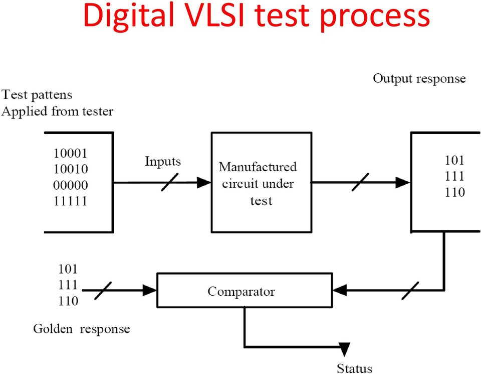
17 Digital VLSI test process
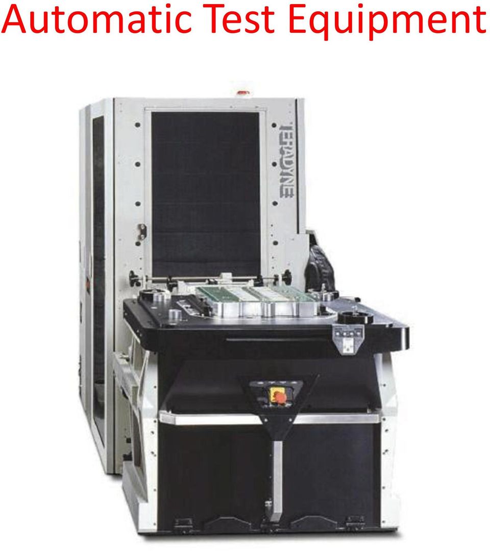
18 Automatic Test Equipment
19 Taxonomy of Digital Testing Criterion When tested? Where is the source of Test patterns? Attributes of testing method 1. Once after manufacture 2. Once before startup of circuit 3. Always during the system operation 1. An external tester 2. Within the chip 3. No patters applied, only monitoring Terminology 1. Manufacturing Test 2. Built in self test (BIST) 3. On-line testing (OLT) 1. Automatic Test Equipment (ATE) based testing 2. BIST 3. OLT
 3.")
20 Taxonomy of Digital Testing Criterion Circuit in which form is being tested? How are the test patterns applied? Attributes of testing method Wafer IC Board System 1. In a fixed predetermined order 2. Depending on results Terminology 1. Non packaged IC level testing 2. Packaged level testing 3. Board level testing 4. System level testing Static Testing Adaptive testing

21 Taxonomy of Digital Testing Criterion Attributes of testing method Terminology How fast are the test patterns applied? Who verifies the test results by matching with golden response? 1. Much slower than the normal speed of operation 2. At normal speed of operation 1. On chip circuit 2. ATE 1. DC (static) testing 2. At-speed testing 1. BIST 2. Automatic Test Equipment (ATE) based testing
22 Test Economics Man hours for test plan development: Expert test engineers to make elaborate test plans. CAD tools for Automatic Test Pattern Generation Cost of ATE ATE is a multimillion dollar instrument. Cost of testing a chip in an ATE is dependent on time a chip is tested, the number of inputs/outputs pins frequency the test patters are to be applied
23 DFT/BIST circuitry Test Economics Additional circuitry kept on-chip to help in testing results in raise in chip area Rise in area power and lower yield At-speed testing by ATE is extremely expensive. Tradeoff Returns Proper binning of Chips: In case of VLSI testing, it is not of much concern as how many chips are binned as faulty, rather important is how many faulty chips are binned as normal. So, economic return from VLSI testing is the accuracy in shipping functionally perfect chips.
24 What we will study? Test Introduction to Digital Testing Lecture-II: Functional vs. Structural Testing Lecture-III: Fault Equivalence, Fault Dominance, Fault Collapsing and Checkpoint Theorem Fault Simulation and Testability Measures Lecture-I and II: Circuit Modeling and Algorithms for Fault Simulation Lecture-III: Combinational SCOAP Measures and Sequential SCOAP Measures Combinational Circuit Test Pattern Generation Lecture-I: Introduction to Automatic Test Pattern Generation (ATPG) and ATPG Algebras Lecture-II: Standard ATPG Algorithms
25 What we will study? Sequential Circuit Testing and Scan Chains Lecture-I: ATPG for Single-Clock Synchronous Circuits Lecture-II and III: Scan Chain based Sequential Circuit Testing Built in Self test (BIST) Lecture I: Introduction to BIST architecture Lecture II and III: Memory BIST
26 Thank you
27 Design Verification and Test of Digital VLSI Circuits NPTEL Video Course Module-VII Lecture-II Functional and Structural Testing
28 Introduction Circuit for Bit wise ANDing Test Pattern Test Pattern Output No Test patterns for functional testing
29 Introduction Need to apply 2 25 test patterns patterns per second (Mega Hz Tester), time required is 33 Seconds per chip. About million chips are to be tested in a run Seconds or Hours or Days or 62 years. Functional Testing cannot be performed due to extremely high testing time.
30 Structural Testing Structural testing, introduced by Eldred, verifies the correctness of the specific structure of the circuit in terms of gates and interconnects Structural Testing takes many fold less time compared Functional Testing yet maintaining the quality of test solution. Structural testing does not check the functionality of the entire circuit rather verifies if all the structural units (gates) are fault free. So structural testing is a kind of functional testing at unit (gate) level.
31 Structural Testing Example Test Pattern Output (OG1) (I1,I2,I3,I4,I5)
32 Structural Testing Example Number of test patterns required are (=160), which is many fold smaller than those required for functional testing (2 25 ). Time required for testing the circuit the using a 1 Mega Hz Tester is seconds and for a million samples is 16 seconds. Structural testing is highly beneficial over functional testing.
33 Structural Testing Penalties Each individual gate is tested; however, the integration is not tested. To test the individual gates, controlling and observing values of intermediary nets in a circuit becomes mandatory, which adds to extra pins and hardware Circuit with about a million internal lines needs a million 2-1 Multiplexers and same number of extra pins. This requirement is infeasible.
34 Structural Testing Penalties
35 Structural Testing With Internal Memory A 32-bit adder requires 2 32 test patterns for exhaustive functional testing.
36 Structural Testing With Internal Memory The 32-bit adder requires 2 3 test patterns for exhaustive structural testing. Extra Pins 3 2 Sets of Registers 2:1 Muxes
37 Structural Testing With Internal Memory Use of internal registers Problem of huge number of extra pins could be solved Added huge size of shift registers (equal to number of internal nets). In a typical circuit there are tens of thousand of internal lines. Efficient structural testing is the one with less number of on-chip components and yet maintaining the quality of test solution. Structural testing with Fault Models is the answer to the requirement ``Structural testing is functional testing at a level lower than the basic inputoutput functionality of the system''. Bitwise ANDing circuit, unit for structural testing--gates 32-bit adder---full adders Digital circuits, structural testing is ``functional testing at the level of gates and flip-flops
38 Structural Testing with Fault Models Structural testing with fault models involves verifying each unit (gate and flip flop) is free from faults of the fault model. A model is an abstract representation of a system. modeling reduces the complexity in representation but captures all the properties of the original system required for the application in question. Fault model is an abstraction of the real defects in the silicon such that the faults of the model are easy to represent should ensure that if one verifies that no faults of the model are in the circuit, quality of test solution is maintained.
39 Structural Testing with Fault Models Unconnected net I1 is the defect. Error is, when I1=1, I2=1,I3=1,I4=1, I5=1 but OG1=0 (should be 1 in normal case). Fault is, net I1 is stuck at 0 (when gate is modeled at binary logic level).
40 Types of Fault Models Stuck-at fault model: Faults are fixed (0 or 1) value to a net. Stuck at-0 and Stuck at-1 single stuck-at fault model Multiple stuck at fault model Delay fault model: Increase the input to output delay of one logic gate, at a time. Bridging Fault: A short between a group of nets AND Bridge OR Bridge
41 Single Stuck-at Fault Model: Fanouts If fanout along with all its branches is a single electrical net, then why fault in a branch does not affect the others? Only one net is faulty at a time. The faulty net is permanently set to either 0 or 1. The branches of a fanout net are independent with respect to locations and affect of a stuck-at fault.
42 Single Stuck-at Fault Model Several stuck-at faults can be simultaneously present in the circuit. A circuit with n lines can have 3 n -1 possible stuck line combinations; each net can be: s-a-1, s-a-0, or faultfree. Handling multiple stuck-at faults in a typical circuit with some hundreds of thousands of nets is infeasible. Single stuck-at fault model is manageable in number and also provides acceptable quality of test solution, it is the most accepted fault model.
43 Structural Testing with Stuck-at Fault Model I1=1, I2=1,.,I25=1, is a test pattern for the stuckat-0 fault at net I1
44 Structural Testing with Stuck-at Fault Model I1=0, I2=1,.,I25=1, is a test pattern for the stuck-at-1 fault at net I1.
45 Structural Testing with Stuck-at Fault Model I1=0, I2=1,.,I25=1, is a test pattern for the stuckat-1 fault at net output of G1. I1=0, I2=1,.,I25=1 tests both s-a-1 at net I1 and output of G1. In structural testing with stuck-at fault model, one test pattern can test more than one fault.
46 Pros and cons for structural testing with stuck-at fault model Pors No extra pin outs or DFT circuitry like 2-1 Multiplexers and shift resisters for controlling and observing internal nets Low test time as one test pattern can test multiple stuck-at faults Cons Functionality is not tested, even for the units (gates and Flip-flops). However, testing history reveals that even with this price paid, quality of test solution is maintained.
47 . Comparison of structural and functional testing Functional testing Without fault models. Manually generated design verification test patterns. Slow and labor intensive. Fault coverage not known More Test Patterns Can be applied at the operating speed. Structural Testing With fault models. Automatic test pattern generation (ATPG). Efficient and automated. Fault Coverage is a quantified metric. Less Test Patterns Difficult to be applied at the speed the design is expected to work.
48 Questions and Answers What are the problems of structural testing without fault models, if the units are as atomic as gates and as large as arithmetic block like 32-bit adder and 64-multiplier How many silicon level defects result in nets getting stuck? Explain relevance of stuck-fault model from that perspective
49 Thank you
50 Design Verification and Test of Digital VLSI Circuits NPTEL Video Course Module-VII Lecture-III Fault Equivalence
51 Introduction If there are n nets in a circuit then there can be 2n stuck-at faults The number of test patterns is liner in the number of nets in a circuit. The total number of test patterns required 2n??
52 Structural Testing with Stuck-at Fault Model I1=0, I2=1,.,I25=1, is a test pattern for the stuck-at-1 fault at net I1.
53 Structural Testing with Stuck-at Fault Model I1=0, I2=1,.,I25=1, is a test pattern for the stuckat-1 fault at net output of G1. I1=0, I2=1,.,I25=1 tests both s-a-1 at net I1 and output of G1. In structural testing with stuck-at fault model, one test pattern can test more than one fault.
54 Fault Equivalence For Single Stuck-At Fault Model Two stuck-at faults f1 and f2 are called equivalent iff the output function represented by the circuit with f1 is same as the output function represented by the circuit with f2. Obviously, equivalent faults have exactly the same set of test patterns. In the AND gate of Figure 1, all stuck-at-0 faults are equivalent as they transform the circuit to O=0 and have I1=1, I2=1 as the test pattern.
55 Fault Equivalence For Single Stuck-At Fault Model All stuck-at-0 faults are equivalent as they transform the circuit to O=0 and have I1=1, I2=1 as the test pattern.
56 Fault Equivalence For Single Stuck-At Fault Model: Fanouts The faults in the stem and branches are not equivalent. Fault at stem results in same output functions of the stem and the branches Fault is in branch I1, then function of stem is I1=0/1 (as driven) and for the branch I1 (I1 ) function is I1 =0 (I1 =I1). Output function of I1 is different from I1 and I1.
57 Fault Equivalence based Collapsing: Example
58 Fault Equivalence based Collapsing: Example
59 Fault Equivalence based Collapsing: Example
60 Fault Equivalence based Collapsing: Example with fanouts
61 Fault Equivalence based Collapsing: Example with fanouts
62 Fault Equivalence based Collapsing: Example with fanouts
63 Fault Dominance For Single Stuck-At Fault Model If all tests of a stuck-at fault f1 detect fault f2 then f2 dominates f1. If f2 dominants f1 then f2 can be removed and only f1is retained.
64 Fault Dominance For Single Stuck-At Fault Model
65 Fault Dominance based Collapsing: Example
66 Fault Dominance based Collapsing: Example
67 Fault Dominance based Collapsing: Example
68 Fault Dominance based Collapsing: Example with fanouts
69 Fault Dominance based Collapsing: Example with fanouts
70 Fault Dominance based Collapsing: Example with fanouts
71 Check point theorem. A circuit with no fanouts, s-a-0 and s-a-1 faults is to be considered only at the primary inputs. So in a fanout free circuit test patters are 2x(Number of primary inputs). For circuit with fanout, checkpoints are primary inputs and fanout branches. Faults are to be kept only on the checkpoints. So a test pattern set that detects all single stuck-at faults of the checkpoints detects all single stuck-at faults in that circuit.
72 Questions and Answers For what class of circuits, maximum benefit is achieved due to fault collapsing and when the benefits are less? What is the typical number for test patterns required to test these classes of circuits? What faults can be collapsed by equivalence in case of XOR gate?
73 Answers
74 Thank you
VLSI Design Verification and Testing
 VLSI Design Verification and Testing Instructor Chintan Patel (Contact using email: [email protected]). Text Michael L. Bushnell and Vishwani D. Agrawal, Essentials of Electronic Testing, for Digital,
Module-I Lecture-I Introduction to Digital VLSI Design Flow
 Design Verification and Test of Digital VLSI Circuits NPTEL Video Course Module-I Lecture-I Introduction to Digital VLSI Design Flow Introduction The functionality of electronics equipments and gadgets
Testing Low Power Designs with Power-Aware Test Manage Manufacturing Test Power Issues with DFTMAX and TetraMAX
 White Paper Testing Low Power Designs with Power-Aware Test Manage Manufacturing Test Power Issues with DFTMAX and TetraMAX April 2010 Cy Hay Product Manager, Synopsys Introduction The most important trend
Digital Circuit Design
 Test and Diagnosis of of ICs Fault coverage (%) 95 9 85 8 75 7 65 97.92 SSL 4,246 Shawn Blanton Professor Department of ECE Center for Silicon System Implementation CMU Laboratory for Integrated Systems
Fault Modeling. Why model faults? Some real defects in VLSI and PCB Common fault models Stuck-at faults. Transistor faults Summary
 Fault Modeling Why model faults? Some real defects in VLSI and PCB Common fault models Stuck-at faults Single stuck-at faults Fault equivalence Fault dominance and checkpoint theorem Classes of stuck-at
Introduction to VLSI Testing
 Introduction to VLSI Testing 李 昆 忠 Kuen-Jong Lee Dept. of Electrical Engineering National Cheng-Kung University Tainan, Taiwan, R.O.C. Introduction to VLSI Testing.1 Problems to Think A 32 bit adder A
Introduction to Digital System Design
 Introduction to Digital System Design Chapter 1 1 Outline 1. Why Digital? 2. Device Technologies 3. System Representation 4. Abstraction 5. Development Tasks 6. Development Flow Chapter 1 2 1. Why Digital
The components. E3: Digital electronics. Goals:
 E3: Digital electronics Goals: Basic understanding of logic circuits. Become familiar with the most common digital components and their use. Equipment: 1 st. LED bridge 1 st. 7-segment display. 2 st. IC
Objective. Testing Principle. Types of Testing. Characterization Test. Verification Testing. VLSI Design Verification and Testing.
 VLSI Design Verification and Testing Objective VLSI Testing Mohammad Tehranipoor Electrical and Computer Engineering University of Connecticut Need to understand Types of tests performed at different stages
1. True or False? A voltage level in the range 0 to 2 volts is interpreted as a binary 1.
 File: chap04, Chapter 04 1. True or False? A voltage level in the range 0 to 2 volts is interpreted as a binary 1. 2. True or False? A gate is a device that accepts a single input signal and produces one
Memory Testing. Memory testing.1
 Memory Testing Introduction Memory Architecture & Fault Models Test Algorithms DC / AC / Dynamic Tests Built-in Self Testing Schemes Built-in Self Repair Schemes Memory testing.1 Memory Market Share in
ECE410 Design Project Spring 2008 Design and Characterization of a CMOS 8-bit Microprocessor Data Path
 ECE410 Design Project Spring 2008 Design and Characterization of a CMOS 8-bit Microprocessor Data Path Project Summary This project involves the schematic and layout design of an 8-bit microprocessor data
Lecture 5: Gate Logic Logic Optimization
 Lecture 5: Gate Logic Logic Optimization MAH, AEN EE271 Lecture 5 1 Overview Reading McCluskey, Logic Design Principles- or any text in boolean algebra Introduction We could design at the level of irsim
Design Verification & Testing Design for Testability and Scan
 Overview esign for testability (FT) makes it possible to: Assure the detection of all faults in a circuit Reduce the cost and time associated with test development Reduce the execution time of performing
Yaffs NAND Flash Failure Mitigation
 Yaffs NAND Flash Failure Mitigation Charles Manning 2012-03-07 NAND flash is one of very few types of electronic device which are knowingly shipped with errors and are expected to generate further errors
CHAPTER 11: Flip Flops
 CHAPTER 11: Flip Flops In this chapter, you will be building the part of the circuit that controls the command sequencing. The required circuit must operate the counter and the memory chip. When the teach
1.Introduction. Introduction. Most of slides come from Semiconductor Manufacturing Technology by Michael Quirk and Julian Serda.
 .Introduction If the automobile had followed the same development cycle as the computer, a Rolls- Royce would today cost $00, get one million miles to the gallon and explode once a year Most of slides
What is a System on a Chip?
 What is a System on a Chip? Integration of a complete system, that until recently consisted of multiple ICs, onto a single IC. CPU PCI DSP SRAM ROM MPEG SoC DRAM System Chips Why? Characteristics: Complex
At-Speed Test Considering Deep Submicron Effects. D. M. H. Walker Dept. of Computer Science Texas A&M University [email protected].
 At-Speed Test Considering Deep Submicron Effects D. M. H. Walker Dept. of Computer Science Teas A&M University [email protected] Integrated Circuit Testing IC Test What s Going On Test Generation Test
Testing of Digital System-on- Chip (SoC)
") Testing of Digital System-on- Chip (SoC) 1 Outline of the Talk Introduction to system-on-chip (SoC) design Approaches to SoC design SoC test requirements and challenges Core test wrapper P1500 core test
Testing of Digital System-on- Chip (SoC) 1 Outline of the Talk Introduction to system-on-chip (SoC) design Approaches to SoC design SoC test requirements and challenges Core test wrapper P1500 core test
Testing & Verification of Digital Circuits ECE/CS 5745/6745. Hardware Verification using Symbolic Computation
 Testing & Verification of Digital Circuits ECE/CS 5745/6745 Hardware Verification using Symbolic Computation Instructor: Priyank Kalla ([email protected]) 3 Credits Mon, Wed, 1:25-2:45pm, WEB L105 Office
Digital Logic Design. Basics Combinational Circuits Sequential Circuits. Pu-Jen Cheng
 Digital Logic Design Basics Combinational Circuits Sequential Circuits Pu-Jen Cheng Adapted from the slides prepared by S. Dandamudi for the book, Fundamentals of Computer Organization and Design. Introduction
Layout of Multiple Cells
 Layout of Multiple Cells Beyond the primitive tier primitives add instances of primitives add additional transistors if necessary add substrate/well contacts (plugs) add additional polygons where needed
Implementation Details
 LEON3-FT Processor System Scan-I/F FT FT Add-on Add-on 2 2 kbyte kbyte I- I- Cache Cache Scan Scan Test Test UART UART 0 0 UART UART 1 1 Serial 0 Serial 1 EJTAG LEON_3FT LEON_3FT Core Core 8 Reg. Windows
Programming Logic controllers
 Programming Logic controllers Programmable Logic Controller (PLC) is a microprocessor based system that uses programmable memory to store instructions and implement functions such as logic, sequencing,
NEW adder cells are useful for designing larger circuits despite increase in transistor count by four per cell.
 CHAPTER 4 THE ADDER The adder is one of the most critical components of a processor, as it is used in the Arithmetic Logic Unit (ALU), in the floating-point unit and for address generation in case of cache
Binary Adders: Half Adders and Full Adders
 Binary Adders: Half Adders and Full Adders In this set of slides, we present the two basic types of adders: 1. Half adders, and 2. Full adders. Each type of adder functions to add two binary bits. In order
Sequential 4-bit Adder Design Report
 UNIVERSITY OF WATERLOO Faculty of Engineering E&CE 438: Digital Integrated Circuits Sequential 4-bit Adder Design Report Prepared by: Ian Hung (ixxxxxx), 99XXXXXX Annette Lo (axxxxxx), 99XXXXXX Pamela
PowerPC Microprocessor Clock Modes
 nc. Freescale Semiconductor AN1269 (Freescale Order Number) 1/96 Application Note PowerPC Microprocessor Clock Modes The PowerPC microprocessors offer customers numerous clocking options. An internal phase-lock
ECE124 Digital Circuits and Systems Page 1
 ECE124 Digital Circuits and Systems Page 1 Chip level timing Have discussed some issues related to timing analysis. Talked briefly about longest combinational path for a combinational circuit. Talked briefly
International Journal of Electronics and Computer Science Engineering 1482
 International Journal of Electronics and Computer Science Engineering 1482 Available Online at www.ijecse.org ISSN- 2277-1956 Behavioral Analysis of Different ALU Architectures G.V.V.S.R.Krishna Assistant
Here we introduced (1) basic circuit for logic and (2)recent nano-devices, and presented (3) some practical issues on nano-devices.
 basic circuit for logic and (2)recent nano-devices, and presented (3) some practical issues on nano-devices.") Outline Here we introduced () basic circuit for logic and (2)recent nano-devices, and presented (3) some practical issues on nano-devices. Circuit Logic Gate A logic gate is an elemantary building block
Outline Here we introduced () basic circuit for logic and (2)recent nano-devices, and presented (3) some practical issues on nano-devices. Circuit Logic Gate A logic gate is an elemantary building block
INTRODUCTION TO DIGITAL SYSTEMS. IMPLEMENTATION: MODULES (ICs) AND NETWORKS IMPLEMENTATION OF ALGORITHMS IN HARDWARE
 AND NETWORKS IMPLEMENTATION OF ALGORITHMS IN HARDWARE") INTRODUCTION TO DIGITAL SYSTEMS 1 DESCRIPTION AND DESIGN OF DIGITAL SYSTEMS FORMAL BASIS: SWITCHING ALGEBRA IMPLEMENTATION: MODULES (ICs) AND NETWORKS IMPLEMENTATION OF ALGORITHMS IN HARDWARE COURSE EMPHASIS:
INTRODUCTION TO DIGITAL SYSTEMS 1 DESCRIPTION AND DESIGN OF DIGITAL SYSTEMS FORMAL BASIS: SWITCHING ALGEBRA IMPLEMENTATION: MODULES (ICs) AND NETWORKS IMPLEMENTATION OF ALGORITHMS IN HARDWARE COURSE EMPHASIS:
Operating Manual Ver.1.1
 4 Bit Binary Ripple Counter (Up-Down Counter) Operating Manual Ver.1.1 An ISO 9001 : 2000 company 94-101, Electronic Complex Pardesipura, Indore- 452010, India Tel : 91-731- 2570301/02, 4211100 Fax: 91-731-
CMOS Binary Full Adder
 CMOS Binary Full Adder A Survey of Possible Implementations Group : Eren Turgay Aaron Daniels Michael Bacelieri William Berry - - Table of Contents Key Terminology...- - Introduction...- 3 - Design Architectures...-
Gates, Circuits, and Boolean Algebra
 Gates, Circuits, and Boolean Algebra Computers and Electricity A gate is a device that performs a basic operation on electrical signals Gates are combined into circuits to perform more complicated tasks
W03 Analysis of DC Circuits. Yrd. Doç. Dr. Aytaç Gören
 W03 Analysis of DC Circuits Yrd. Doç. Dr. Aytaç Gören ELK 2018 - Contents W01 Basic Concepts in Electronics W02 AC to DC Conversion W03 Analysis of DC Circuits (self and condenser) W04 Transistors and
ELEC 2210 - EXPERIMENT 1 Basic Digital Logic Circuits
 Objectives ELEC - EXPERIMENT Basic Digital Logic Circuits The experiments in this laboratory exercise will provide an introduction to digital electronic circuits. You will learn how to use the IDL-00 Bit
Digital Electronics Detailed Outline
 Digital Electronics Detailed Outline Unit 1: Fundamentals of Analog and Digital Electronics (32 Total Days) Lesson 1.1: Foundations and the Board Game Counter (9 days) 1. Safety is an important concept
CHAPTER 3 Boolean Algebra and Digital Logic
 CHAPTER 3 Boolean Algebra and Digital Logic 3.1 Introduction 121 3.2 Boolean Algebra 122 3.2.1 Boolean Expressions 123 3.2.2 Boolean Identities 124 3.2.3 Simplification of Boolean Expressions 126 3.2.4
Encounter DFT Architect
 Full-chip, synthesis-based, power-aware test architecture development Cadence Encounter DFT Architect addresses and optimizes multiple design and manufacturing objectives such as timing, area, wiring,
Computer Systems Structure Main Memory Organization
 Computer Systems Structure Main Memory Organization Peripherals Computer Central Processing Unit Main Memory Computer Systems Interconnection Communication lines Input Output Ward 1 Ward 2 Storage/Memory
EE411: Introduction to VLSI Design Course Syllabus
 : Introduction to Course Syllabus Dr. Mohammad H. Awedh Spring 2008 Course Overview This is an introductory course which covers basic theories and techniques of digital VLSI design in CMOS technology.
TABLE OF CONTENTS. xiii List of Tables. xviii List of Design-for-Test Rules. xix Preface to the First Edition. xxi Preface to the Second Edition
 TABLE OF CONTENTS List of Figures xiii List of Tables xviii List of Design-for-Test Rules xix Preface to the First Edition xxi Preface to the Second Edition xxiii Acknowledgement xxv 1 Boundary-Scan Basics
University of Texas at Dallas. Department of Electrical Engineering. EEDG 6306 - Application Specific Integrated Circuit Design
 University of Texas at Dallas Department of Electrical Engineering EEDG 6306 - Application Specific Integrated Circuit Design Synopsys Tools Tutorial By Zhaori Bi Minghua Li Fall 2014 Table of Contents
Application Of Build-in Self Test In Functional Test Of DSL
 Application Of Build-in Self Test In Functional Test Of DSL YaJun Gu, Ye Qin, ZhiJun Wang, David Wei, Andrew Ho, Stephen Chen, Zhen (Jane) Feng Ph. D., Murad Kurwa No.77 Yong Sheng Road, Malu, Jiading,
Low Power AMD Athlon 64 and AMD Opteron Processors
 Low Power AMD Athlon 64 and AMD Opteron Processors Hot Chips 2004 Presenter: Marius Evers Block Diagram of AMD Athlon 64 and AMD Opteron Based on AMD s 8 th generation architecture AMD Athlon 64 and AMD
GETTING STARTED WITH PROGRAMMABLE LOGIC DEVICES, THE 16V8 AND 20V8
 GETTING STARTED WITH PROGRAMMABLE LOGIC DEVICES, THE 16V8 AND 20V8 Robert G. Brown All Rights Reserved August 25, 2000 Alta Engineering 58 Cedar Lane New Hartford, CT 06057-2905 (860) 489-8003 www.alta-engineering.com
Efficient Interconnect Design with Novel Repeater Insertion for Low Power Applications
 Efficient Interconnect Design with Novel Repeater Insertion for Low Power Applications TRIPTI SHARMA, K. G. SHARMA, B. P. SINGH, NEHA ARORA Electronics & Communication Department MITS Deemed University,
Introduction to CMOS VLSI Design (E158) Lecture 8: Clocking of VLSI Systems
 Lecture 8: Clocking of VLSI Systems") Harris Introduction to CMOS VLSI Design (E158) Lecture 8: Clocking of VLSI Systems David Harris Harvey Mudd College [email protected] Based on EE271 developed by Mark Horowitz, Stanford University MAH
Harris Introduction to CMOS VLSI Design (E158) Lecture 8: Clocking of VLSI Systems David Harris Harvey Mudd College [email protected] Based on EE271 developed by Mark Horowitz, Stanford University MAH
Lecture 7: Clocking of VLSI Systems
 Lecture 7: Clocking of VLSI Systems MAH, AEN EE271 Lecture 7 1 Overview Reading Wolf 5.3 Two-Phase Clocking (good description) W&E 5.5.1, 5.5.2, 5.5.3, 5.5.4, 5.5.9, 5.5.10 - Clocking Note: The analysis
Counters and Decoders
 Physics 3330 Experiment #10 Fall 1999 Purpose Counters and Decoders In this experiment, you will design and construct a 4-bit ripple-through decade counter with a decimal read-out display. Such a counter
ASYNCHRONOUS COUNTERS
 LB no.. SYNCHONOUS COUNTES. Introduction Counters are sequential logic circuits that counts the pulses applied at their clock input. They usually have 4 bits, delivering at the outputs the corresponding
Chapter 2 Logic Gates and Introduction to Computer Architecture
 Chapter 2 Logic Gates and Introduction to Computer Architecture 2.1 Introduction The basic components of an Integrated Circuit (IC) is logic gates which made of transistors, in digital system there are
e.g. τ = 12 ps in 180nm, 40 ps in 0.6 µm Delay has two components where, f = Effort Delay (stage effort)= gh p =Parasitic Delay
= gh p =Parasitic Delay") Logic Gate Delay Chip designers need to choose: What is the best circuit topology for a function? How many stages of logic produce least delay? How wide transistors should be? Logical Effort Helps make
Logic Gate Delay Chip designers need to choose: What is the best circuit topology for a function? How many stages of logic produce least delay? How wide transistors should be? Logical Effort Helps make
ISSN: 2319-5967 ISO 9001:2008 Certified International Journal of Engineering Science and Innovative Technology (IJESIT) Volume 2, Issue 3, May 2013
 Volume 2, Issue 3, May 2013") Transistor Level Fault Finding in VLSI Circuits using Genetic Algorithm Lalit A. Patel, Sarman K. Hadia CSPIT, CHARUSAT, Changa., CSPIT, CHARUSAT, Changa Abstract This paper presents, genetic based algorithm
Transistor Level Fault Finding in VLSI Circuits using Genetic Algorithm Lalit A. Patel, Sarman K. Hadia CSPIT, CHARUSAT, Changa., CSPIT, CHARUSAT, Changa Abstract This paper presents, genetic based algorithm
INSTITUTE OF AERONAUTICAL ENGINEERING Dundigal, Hyderabad - 500 043
 INSTITUTE OF AERONAUTICAL ENGINEERING Dundigal, Hyderabad - 500 043 ELECTRONICS AND COMMUNICATION ENGINEERING Course Title VLSI DESIGN Course Code 57035 Regulation R09 COURSE DESCRIPTION Course Structure
Chapter 10 Advanced CMOS Circuits
 Transmission Gates Chapter 10 Advanced CMOS Circuits NMOS Transmission Gate The active pull-up inverter circuit leads one to thinking about alternate uses of NMOS devices. Consider the circuit shown in
Agenda. Michele Taliercio, Il circuito Integrato, Novembre 2001
 Agenda Introduzione Il mercato Dal circuito integrato al System on a Chip (SoC) La progettazione di un SoC La tecnologia Una fabbrica di circuiti integrati 28 How to handle complexity G The engineering
1.1 Silicon on Insulator a brief Introduction
 Table of Contents Preface Acknowledgements Chapter 1: Overview 1.1 Silicon on Insulator a brief Introduction 1.2 Circuits and SOI 1.3 Technology and SOI Chapter 2: SOI Materials 2.1 Silicon on Heteroepitaxial
NAND Flash FAQ. Eureka Technology. apn5_87. NAND Flash FAQ
 What is NAND Flash? What is the major difference between NAND Flash and other Memory? Structural differences between NAND Flash and NOR Flash What does NAND Flash controller do? How to send command to
Memory Elements. Combinational logic cannot remember
 Memory Elements Combinational logic cannot remember Output logic values are function of inputs only Feedback is needed to be able to remember a logic value Memory elements are needed in most digital logic
Introduction to CMOS VLSI Design
 Introduction to CMOS VLSI esign Slides adapted from: N. Weste,. Harris, CMOS VLSI esign, Addison-Wesley, 3/e, 24 Introduction Integrated Circuits: many transistors on one chip Very Large Scale Integration
Analog & Digital Electronics Course No: PH-218
 Analog & Digital Electronics Course No: PH-218 Lec-28: Logic Gates & Family Course Instructor: Dr. A. P. VAJPEYI Department of Physics, Indian Institute of Technology Guwahati, India 1 Digital Logic Gates
Lecture 8: Synchronous Digital Systems
 Lecture 8: Synchronous Digital Systems The distinguishing feature of a synchronous digital system is that the circuit only changes in response to a system clock. For example, consider the edge triggered
Example-driven Interconnect Synthesis for Heterogeneous Coarse-Grain Reconfigurable Logic
 Example-driven Interconnect Synthesis for Heterogeneous Coarse-Grain Reconfigurable Logic Clifford Wolf, Johann Glaser, Florian Schupfer, Jan Haase, Christoph Grimm Computer Technology /99 Overview Ultra-Low-Power
Understanding Logic Design
 Understanding Logic Design ppendix of your Textbook does not have the needed background information. This document supplements it. When you write add DD R0, R1, R2, you imagine something like this: R1
A Digital Timer Implementation using 7 Segment Displays
 A Digital Timer Implementation using 7 Segment Displays Group Members: Tiffany Sham u2548168 Michael Couchman u4111670 Simon Oseineks u2566139 Caitlyn Young u4233209 Subject: ENGN3227 - Analogue Electronics
Low-resolution Image Processing based on FPGA
 Abstract Research Journal of Recent Sciences ISSN 2277-2502. Low-resolution Image Processing based on FPGA Mahshid Aghania Kiau, Islamic Azad university of Karaj, IRAN Available online at: www.isca.in,
ESP-CV Custom Design Formal Equivalence Checking Based on Symbolic Simulation
 Datasheet -CV Custom Design Formal Equivalence Checking Based on Symbolic Simulation Overview -CV is an equivalence checker for full custom designs. It enables efficient comparison of a reference design
Pass Gate Logic An alternative to implementing complex logic is to realize it using a logic network of pass transistors (switches).
.") Pass Gate Logic n alternative to implementing complex logic is to realize it using a logic network of pass transistors (switches). Switch Network Regeneration is performed via a buffer. We have already
Pass Gate Logic n alternative to implementing complex logic is to realize it using a logic network of pass transistors (switches). Switch Network Regeneration is performed via a buffer. We have already
NAME AND SURNAME. TIME: 1 hour 30 minutes 1/6
 E.T.S.E.T.B. MSc in ICT FINAL EXAM VLSI Digital Design Spring Course 2005-2006 June 6, 2006 Score publication date: June 19, 2006 Exam review request deadline: June 22, 2006 Academic consultancy: June
Evaluating AC Current Sensor Options for Power Delivery Systems
 Evaluating AC Current Sensor Options for Power Delivery Systems State-of-the-art isolated ac current sensors based on CMOS technology can increase efficiency, performance and reliability compared to legacy
Testing and Programming PCBA s during Design and in Production
 Testing and Programming PCBA s during Design and in Production Hogeschool van Arnhem en Nijmegen 6 June 23 Rob Staals JTAG Technologies [email protected] Copyright 23, JTAG Technologies juni 3 The importance
9/14/2011 14.9.2011 8:38
 Algorithms and Implementation Platforms for Wireless Communications TLT-9706/ TKT-9636 (Seminar Course) BASICS OF FIELD PROGRAMMABLE GATE ARRAYS Waqar Hussain [email protected] Department of Computer
Combinational Controllability Controllability Formulas (Cont.)
") Outline Digital Testing: Testability Measures The case for DFT Testability Measures Controllability and observability SCOA measures Combinational circuits Sequential circuits Adhoc techniques Easily testable
Outline Digital Testing: Testability Measures The case for DFT Testability Measures Controllability and observability SCOA measures Combinational circuits Sequential circuits Adhoc techniques Easily testable
Clocking. Figure by MIT OCW. 6.884 - Spring 2005 2/18/05 L06 Clocks 1
 ing Figure by MIT OCW. 6.884 - Spring 2005 2/18/05 L06 s 1 Why s and Storage Elements? Inputs Combinational Logic Outputs Want to reuse combinational logic from cycle to cycle 6.884 - Spring 2005 2/18/05
ETEC 2301 Programmable Logic Devices. Chapter 10 Counters. Shawnee State University Department of Industrial and Engineering Technologies
 ETEC 2301 Programmable Logic Devices Chapter 10 Counters Shawnee State University Department of Industrial and Engineering Technologies Copyright 2007 by Janna B. Gallaher Asynchronous Counter Operation
ON SUITABILITY OF FPGA BASED EVOLVABLE HARDWARE SYSTEMS TO INTEGRATE RECONFIGURABLE CIRCUITS WITH HOST PROCESSING UNIT
 216 ON SUITABILITY OF FPGA BASED EVOLVABLE HARDWARE SYSTEMS TO INTEGRATE RECONFIGURABLE CIRCUITS WITH HOST PROCESSING UNIT *P.Nirmalkumar, **J.Raja Paul Perinbam, @S.Ravi and #B.Rajan *Research Scholar,
PMOS Testing at Rochester Institute of Technology Dr. Lynn Fuller
 ROCHESER INSIUE OF ECHNOLOGY MICROELECRONIC ENGINEERING PMOS esting at Dr. Lynn Fuller webpage: http://www.rit.edu/~lffeee 82 Lomb Memorial Drive Rochester, NY 14623-5604 el (585) 475-2035 Fax (585) 475-5041
Sequential Logic Design Principles.Latches and Flip-Flops
 Sequential Logic Design Principles.Latches and Flip-Flops Doru Todinca Department of Computers Politehnica University of Timisoara Outline Introduction Bistable Elements Latches and Flip-Flops S-R Latch
State-of-Art (SoA) System-on-Chip (SoC) Design HPC SoC Workshop
 System-on-Chip (SoC) Design HPC SoC Workshop") Photos placed in horizontal position with even amount of white space between photos and header State-of-Art (SoA) System-on-Chip (SoC) Design HPC SoC Workshop Michael Holmes Manager, Mixed Signal ASIC/SoC
Photos placed in horizontal position with even amount of white space between photos and header State-of-Art (SoA) System-on-Chip (SoC) Design HPC SoC Workshop Michael Holmes Manager, Mixed Signal ASIC/SoC
System-on. on-chip Design Flow. Prof. Jouni Tomberg Tampere University of Technology Institute of Digital and Computer Systems. jouni.tomberg@tut.
 System-on on-chip Design Flow Prof. Jouni Tomberg Tampere University of Technology Institute of Digital and Computer Systems [email protected] 26.03.2003 Jouni Tomberg / TUT 1 SoC - How and with whom?
Optimization and Comparison of 4-Stage Inverter, 2-i/p NAND Gate, 2-i/p NOR Gate Driving Standard Load By Using Logical Effort
 Optimization and Comparison of -Stage, -i/p NND Gate, -i/p NOR Gate Driving Standard Load By Using Logical Effort Satyajit nand *, and P.K.Ghosh ** * Mody Institute of Technology & Science/ECE, Lakshmangarh,
Logic in Computer Science: Logic Gates
 Logic in Computer Science: Logic Gates Lila Kari The University of Western Ontario Logic in Computer Science: Logic Gates CS2209, Applied Logic for Computer Science 1 / 49 Logic and bit operations Computers
Electrical Safety Tester Verification
 Ensuring Validity of Regulatory Tests Verification of electrical safety testing equipment is a procedure that is often overlooked by manufacturers. Running test verification is crucial to ensuring that
NTE2053 Integrated Circuit 8 Bit MPU Compatible A/D Converter
 NTE2053 Integrated Circuit 8 Bit MPU Compatible A/D Converter Description: The NTE2053 is a CMOS 8 bit successive approximation Analog to Digital converter in a 20 Lead DIP type package which uses a differential
Let s put together a Manual Processor
 Lecture 14 Let s put together a Manual Processor Hardware Lecture 14 Slide 1 The processor Inside every computer there is at least one processor which can take an instruction, some operands and produce
Gates & Boolean Algebra. Boolean Operators. Combinational Logic. Introduction
 Introduction Gates & Boolean lgebra Boolean algebra: named after mathematician George Boole (85 864). 2-valued algebra. digital circuit can have one of 2 values. Signal between and volt =, between 4 and
3D NAND Technology Implications to Enterprise Storage Applications
 3D NAND Technology Implications to Enterprise Storage Applications Jung H. Yoon Memory Technology IBM Systems Supply Chain Outline Memory Technology Scaling - Driving Forces Density trends & outlook Bit
WEEK 8.1 Registers and Counters. ECE124 Digital Circuits and Systems Page 1
 WEEK 8.1 egisters and Counters ECE124 igital Circuits and Systems Page 1 Additional schematic FF symbols Active low set and reset signals. S Active high set and reset signals. S ECE124 igital Circuits
The Evolution of ICT: PCB Technologies, Test Philosophies, and Manufacturing Business Models Are Driving In-Circuit Test Evolution and Innovations
 The Evolution of ICT: PCB Technologies, Test Philosophies, and Manufacturing Business Models Are Driving In-Circuit Test Evolution and Innovations Alan J. Albee Teradyne Inc. North Reading, Massachusetts
ANALOG & DIGITAL ELECTRONICS
 ANALOG & DIGITAL ELECTRONICS Course Instructor: Course No: PH-218 3-1-0-8 Dr. A.P. Vajpeyi E-mail: [email protected] Room No: #305 Department of Physics, Indian Institute of Technology Guwahati,
Using a Failure Modes, Effects and Diagnostic Analysis (FMEDA) to Measure Diagnostic Coverage in Programmable Electronic Systems.
 to Measure Diagnostic Coverage in Programmable Electronic Systems.") Using a Failure Modes, Effects and Diagnostic Analysis (FMEDA) to Measure Diagnostic Coverage in Programmable Electronic Systems. Dr. William M. Goble exida.com, 42 Short Rd., Perkasie, PA 18944 Eindhoven
Using a Failure Modes, Effects and Diagnostic Analysis (FMEDA) to Measure Diagnostic Coverage in Programmable Electronic Systems. Dr. William M. Goble exida.com, 42 Short Rd., Perkasie, PA 18944 Eindhoven
Experiment # 9. Clock generator circuits & Counters. Eng. Waleed Y. Mousa
 Experiment # 9 Clock generator circuits & Counters Eng. Waleed Y. Mousa 1. Objectives: 1. Understanding the principles and construction of Clock generator. 2. To be familiar with clock pulse generation
AN IMPROVED DESIGN OF REVERSIBLE BINARY TO BINARY CODED DECIMAL CONVERTER FOR BINARY CODED DECIMAL MULTIPLICATION
 American Journal of Applied Sciences 11 (1): 69-73, 2014 ISSN: 1546-9239 2014 Science Publication doi:10.3844/ajassp.2014.69.73 Published Online 11 (1) 2014 (http://www.thescipub.com/ajas.toc) AN IMPROVED
PLL frequency synthesizer
 ANALOG & TELECOMMUNICATION ELECTRONICS LABORATORY EXERCISE 4 Lab 4: PLL frequency synthesizer 1.1 Goal The goals of this lab exercise are: - Verify the behavior of a and of a complete PLL - Find capture