Decorative vacuum coating technologies Certottica Longarone. Thin Film Plasma Coating Technologies
|
|
|
- Magdalen Armstrong
- 8 years ago
- Views:
Transcription
1 Dr. Stefan Schlichtherle Dr. Georg Strauss PhysTech Coating Technology GmbH Decorative vacuum coating technologies Certottica Longarone Thin Film Plasma Coating Technologies

2 Content The fascination of functional surfaces produced by thin film technology Presentation of PhysTech Typical applications and examples Functional surfaces PVD (Physical Vapour Deposition) technology Some realised examples
 technology Some realised")
3 PhysTech

4 Thin Film Technology Functionalising of surfaces by PVD technologies Thin films produced by PVD technologies can show a lot of specific properties from nm to µm they make tools hard and wear resistant they transmit, reflect or filter light they protect and decorate surfaces they isolate against heat or coldness they improve electric conductivity they realise diffusion barriers

5 Thin Film Technology Tribology Optics Surface protection Tools Medical Implantats Electronics...

6 PVD technology Coating material transfer mechanisms Three fundamental mechanisms Evaporation Sputtering Exploding Plasma Ablation E-gun for evaporation magnetron plasma arc source deposition

7 PVD technology Evaporation Sputtering - Ablation working gas, e.g. Ar Transport of particles in the plasma electrons Ions +/- Condensation Bias atoms molecules Starting material: Targets, cathodes, granulate, ingots, tabs radicals Gas phase: Plasma reactive gas, e.g. O 2, N 2 Substrate: Glass, metal, plastic

8 PVD technology solid liquid gaseous plasma energy/temperature gas molecules gas molecules excited Ions molecule fragments highly excited free electrons

9 PVD technology Different plasmas in pvd technologies

10 PVD technology Balzers/Evatec BAP 800 Leybold APS 900/1100 Optical Interference Coatings, N. Kaiser, H.K. Pulker, (Eds.), Springer, 2003

11 PVD technology Balanced magnetron configuration Characteristics of Sputtering Sputter Threshold Sputter Yield Sputter Rate Non reactive reactive process Unbalanced magnetron configuration Sputtering variants dc magnetron sputtering dc pulsed magnetron sputtering rf sputtering dual beam sputtering ion beam sputtering closed field sputtering

12 PVD technology Scematic of a magnetron sputter process

13 PVD technology Different voltage configuration in DC-PMS

14 PVD technology Electrical schematic of a pulse generator AE Pinnacle Plus 5kW: 0-350kHz pulse generator

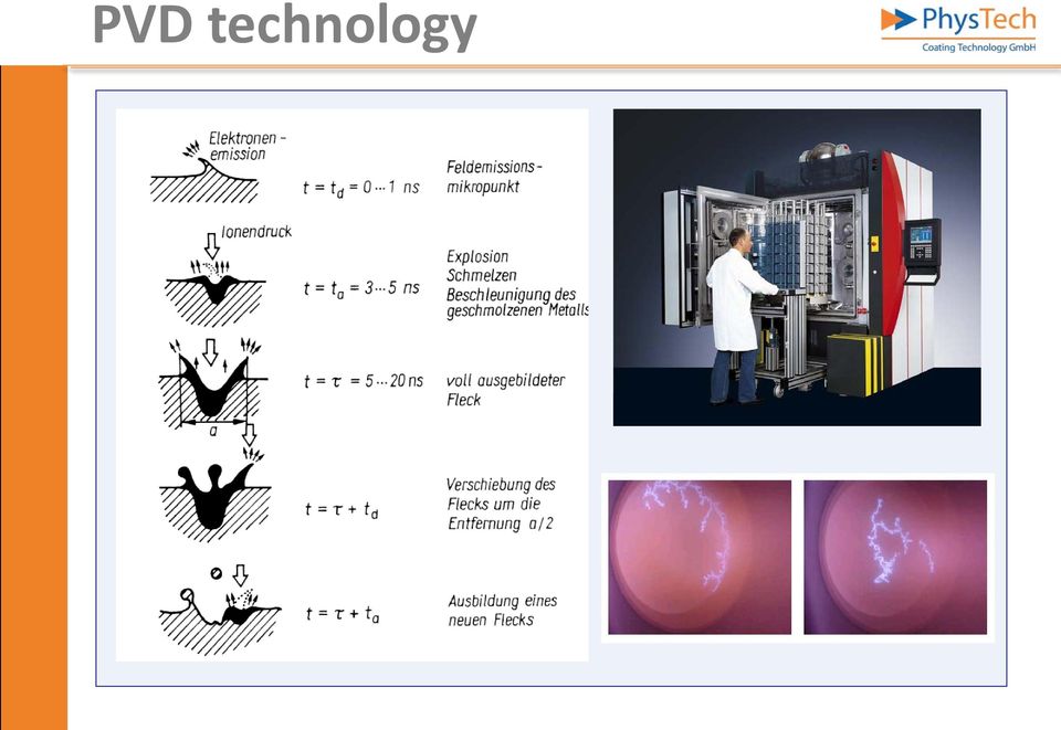
15 PVD technology 1 substrate holder 2 arc sources - cathodes 3 vacumm pumping system 4 gas inlet system 5 gas inlet system 6 substrates, products

16 PVD technology
17 PVD technology Macroparticle filter, LBNL, Berkeley Particle separation with magnetic systems (Droplets, Makropartikel)

18 PVD process analysis Plasmamonitorsystem PPM421 (Inficon) differential pumped mass spectrometer with additional energy analyser (CMA) detection of ions and neutrals measurement of the ion energy distribution of the relevant process ions detection unit: SEV pressure range: up to 10-1 mbar

19 PVD process analysis Langmuir Probe System (Scientific Instruments) trigger acquisition electronics gabing electronics for boxcar mode (100 khz) an electrical conductable and heatable electrode is inserted into the plasma measurement of the voltagecurrent characteristic and calculation of plasma parameters as particle densities, electrical potentials and ion currents relative simple configuration Plasma langmuir probe Principle setup

20 PVD process analysis Ion energy distribution and degree of ionisation Evaporation: Magnetron Sputtering DC Pulsed Sputtering IBAD DC Pulsed Sputtering PLAD, ARC Source

21 PVD process analysis Surface reactions and bombardement effects energetic particle reflected ions or neutrals secondary electrons sputtered atoms or ions surface adsorbed surface species surface region enhanced surface mobility lattice defects trapping displacement enhanced chemical reactions redeposited implanted channeling collision cascade backsputtered surface near surface region Schematic of energetic particles, which bombard the growing film (bombardement) Surface: Interface between solid material and gas (vapour or vacuum) Surface region: depth of penetration of the bombarding particles Near surface region: region below depth of penetration, but is also influenced by e.g. Heating or diffusion Bulk region: region were the material is not influenced by the bombarding effects
22 PVD process analysis Surface reactions and bombardement effects The effects of bombardment of energetic species (ions, neutrals) on the surface and the surface region include: desorption of weakly bonded surface species ejection of secondary electrons reflection of the energetic species as high energetic neutrals sputter ejection of surface atoms by momentum transfer through collision cascades sputtering and re-deposition of sputtered species enhanced mobility of surface atoms enhanced chemical reaction of impinging and adsorbed species. In the subsurface region the impinging particles may be physically implanted the collision cascades cause displacement of atoms and the creation of lattice defects surface species may be recoil-implanted into the surface lattice mobile species may be trapped at lattice defects particle kinetic energy is mostly converted into heat
23 PVD process analysis Ti+ ions cps dc Process parameters: kHz Distance to Ti target: 20cm Pulse frequency: 50kHz - 250kHz 100kHz Pulse width: 1296ns 250kHz I=0,5A p 10 4 tot =3,4*10-3 mbar - 5*10-3 mbar P el =67W - 162W Ar flow =210sccm N flow 2 =30sccm energy in ev Ion energy distribution in a TiN DC-pulsed Magnetron process
24 PVD process analysis 7 10 Ti+ ions Process parameters: I arc =85A Arc target Ti (distance=20cm) P 10 6 N2 variable p tot =1*10-3 mbar p tot =1*10-2 mbar 10 5 p tot =1*10-1 mbar cps energy in ev Ion energy distribution in a TiN Arc Source process
25 PVD process analysis Power density on target E kin of particles Beam velocity Deposition rate Current density on substrate e-gun evaporation Reactive Low Voltage Ion Plating Magnetron sputtering Ion beam sputtering Wcm 4 2 met 3 2 Wcmdiel 4 2 > 10 Wcm ev < 0,3 ev ms High High 2 0, 2 1 macm > 10 Wcm ev Medium 2 0,1 macm > 10 Wcm ev ms Low Medium 2 0,5 1 macm Pulsed laser ablation Arc source ablation Wcm ev ms High 2 > 1 macm Wcm ev ms High 2 > 1 macm
26 PVD film growth
27 PVD film properties Einstellung von Schichteigenschaften Stoichiometry Purity Structure Microstructure Homogeneity Isotropy Topography Density Adherence Hardness Abrasion resistance Stress Anforderungen an optische Schichten: Reproduzierbare und stabile Brechungsindexe Geringe optische Verluste Oberflächenschutz vor Flüssigkeiten, Gasen, Festkörperteilchen, Strahlung Abhängigkeit der Dichte abhängigen Eigenschaften von der kinetischen Energie der bombardierenden Teilchen für verschiedene Prozesstechnologien
28 PVD process technologies Correlation: process parameters plasma properties - film properties Process parameter: process pressure, target material, target power density, applied currents and voltages, pulse frequency and duty cycle Plasma properties: Kinetic energy of ions Ion current density Film properties: Density and morphology of films Oxide films for optical applications Nitride films for tribological and tool applications Refractive index Adhesion Mechanical stress Mechanical stress Optical loss Hardness
29 PVD technology Arc Source Deposition (PhysTech)
30 PVD technology Magnetron Sputter Coater (Edwards)
31 PVD technology Gas-Flow-Sputtering (PhysTech)
32 Research activities EMPA Dübendorf (CH) CeTeV Carsoli (I)
33 Research activities IonBond Newcastle (GB)
34 Thank you for your attention
35 Typical applications Activation of plastic parts Magnetron sputter plasma for the deposition of optical thin films HIPIMS High Plasma Impuls Magnetron Sputtering Deposition of tribological and hard coatings Filtered Arc Source Deposition of hard coatings
36 Typical applications Arc Source Deposition Innova - Balzers Tools Tribology Surface protection Corrosion protection by atmospheric plasma deposition Arc Source Plasma atmospheric plasma deposition increases the polarity of the plastic surface increased adhesion Cleaning of metal parts by plasma pre-treatments
37 Typical applications Plasmapolymerisation treatment of temperature sensitive parts and realisation of specific surface properties like anti-finger-printing, easy to clean, anti-adhesion Pulsed magnetron sputtering for architectual glass coating Decorative hard coatings, z.b. TiN, TiAlN, CrN
38 Typical applications Ion beam assisted deposition for deposition of High precision optical interference coatings APS advanced plasma source Deposition of optical multilayer systems
39 Typical applications Plasmanitrieren: Plasma nitriding is a thermo-chemical process to modify surfaces and barrier layers. It is based on the incorporation of nitrogen into the surface of the component. Process gases are: ammonia, nitrogen, methane and hydrogen. Plasma nitriding takes place in a vacuum chamber under ionic gas atmosphere. To produce wear resistant films sometimes a mixed gas atmosphere is used. The quality of the nitrided surface is dependent on the gas mixture, pressure, temperature and process time. Applications: tools, mechanical components, winds, engine parts like crank shafts, camshafts or valves
2. Deposition process
 Properties of optical thin films produced by reactive low voltage ion plating (RLVIP) Antje Hallbauer Thin Film Technology Institute of Ion Physics & Applied Physics University of Innsbruck Investigations
Coating Technology: Evaporation Vs Sputtering
 Satisloh Italy S.r.l. Coating Technology: Evaporation Vs Sputtering Gianni Monaco, PhD R&D project manager, Satisloh Italy 04.04.2016 V1 The aim of this document is to provide basic technical information
Vacuum Evaporation Recap
 Sputtering Vacuum Evaporation Recap Use high temperatures at high vacuum to evaporate (eject) atoms or molecules off a material surface. Use ballistic flow to transport them to a substrate and deposit.
QGA Quantitative Gas Analyser
 QGA Quantitative Gas Analyser A compact bench-top system for real-time gas and vapour analysis Detailed product information / introduction catalysis studies environmental gas analysis fermentation off-gas
Neuere Entwicklungen zur Herstellung optischer Schichten durch reaktive. Wolfgang Hentsch, Dr. Reinhard Fendler. FHR Anlagenbau GmbH
 Neuere Entwicklungen zur Herstellung optischer Schichten durch reaktive Sputtertechnologien Wolfgang Hentsch, Dr. Reinhard Fendler FHR Anlagenbau GmbH Germany Contents: 1. FHR Anlagenbau GmbH in Brief
Reactive Sputtering Using a Dual-Anode Magnetron System
 Reactive Sputtering Using a Dual-Anode Magnetron System A. Belkind and Z. Zhao, Stevens Institute of Technology, Hoboken, NJ; and D. Carter, G. McDonough, G. Roche, and R. Scholl, Advanced Energy Industries,
A Remote Plasma Sputter Process for High Rate Web Coating of Low Temperature Plastic Film with High Quality Thin Film Metals and Insulators
 A Remote Plasma Sputter Process for High Rate Web Coating of Low Temperature Plastic Film with High Quality Thin Film Metals and Insulators Dr Peter Hockley and Professor Mike Thwaites, Plasma Quest Limited
How To Make A Plasma Control System
 XXII. Erfahrungsaustausch Mühlleiten 2015 Plasmaanalyse und Prozessoptimierung mittels spektroskopischem Plasmamonitoring in industriellen Anwendungen Swen Marke,, Lichtenau Thomas Schütte, Plasus GmbH,
Plasma Electronic is Partner of. Tailor-Made Surfaces by Plasma Technology
 Precision Fair 2013 Stand 171 Plasma Electronic is Partner of Tailor-Made Surfaces by Plasma Technology Dr. J. Geng, Plasma Electronic GmbH Modern Surface Technology in 1900 Overview A short introduction
Deposition of Thin Metal Films " (on Polymer Substrates)!
!") Deposition of Thin Metal Films " (on Polymer Substrates)! Shefford P. Baker! Cornell University! Department of Materials Science and Engineering! Ithaca, New York, 14853! MS&E 5420 Flexible Electronics,
Deposition of Thin Metal Films " (on Polymer Substrates)! Shefford P. Baker! Cornell University! Department of Materials Science and Engineering! Ithaca, New York, 14853! MS&E 5420 Flexible Electronics,
Chemical Sputtering. von Kohlenstoff durch Wasserstoff. W. Jacob
 Chemical Sputtering von Kohlenstoff durch Wasserstoff W. Jacob Centre for Interdisciplinary Plasma Science Max-Planck-Institut für Plasmaphysik, 85748 Garching Content: Definitions: Chemical erosion, physical
Introduction to Thin Film Technology LOT. Chair of Surface and Materials Technology
 Introduction to Thin Film Introduction to Thin Film Verfahrenstechnik der Oberflächenmodifikationen Prof. Dr. Xin Jiang Lecture Institut für Werkstofftechnik der Uni-Siegen Sommersemester 2007 Introduction
State of the art in reactive magnetron sputtering
 State of the art in reactive magnetron sputtering T. Nyberg, O. Kappertz, T. Kubart and S. Berg Solid State Electronics, The Ångström Laboratory, Uppsala University, Box 534, S-751 21 Uppsala, Sweden D.
and LUMINOUS CHEMICAL VAPOR DEPOSITION INTERFACE ENGINEERING HirotsuguYasuda University of Missouri-Columbia Columbia, Missouri, U.S.A.
 LUMINOUS CHEMICAL VAPOR DEPOSITION and INTERFACE ENGINEERING HirotsuguYasuda University of Missouri-Columbia Columbia, Missouri, U.S.A. MARCEL MARCEL DEKKER. NEW YORK DEKKER Contents Preface iii Part I.
High Rate Oxide Deposition onto Web by Reactive Sputtering from Rotatable Magnetrons
 High Rate Oxide Deposition onto Web by Reactive Sputtering from Rotatable Magnetrons D.Monaghan, V. Bellido-Gonzalez, M. Audronis. B. Daniel Gencoa, Physics Rd, Liverpool, L24 9HP, UK. www.gencoa.com,
Lecture 12. Physical Vapor Deposition: Evaporation and Sputtering Reading: Chapter 12. ECE 6450 - Dr. Alan Doolittle
 Lecture 12 Physical Vapor Deposition: Evaporation and Sputtering Reading: Chapter 12 Evaporation and Sputtering (Metalization) Evaporation For all devices, there is a need to go from semiconductor to metal.
1. Photon Beam Damage and Charging at Solid Surfaces John H. Thomas III
 1. Photon Beam Damage and Charging at Solid Surfaces John H. Thomas III 1. Introduction............................. 2. Electrostatic Charging of Samples in Photoemission Experiments............................
Plasma Cleaner: Physics of Plasma
 Plasma Cleaner: Physics of Plasma Nature of Plasma A plasma is a partially ionized gas consisting of electrons, ions and neutral atoms or molecules The plasma electrons are at a much higher temperatures
THIN FILM MATERIALS TECHNOLOGY
 THIN FILM MATERIALS TECHNOLOGY Sputtering of Compound Materials by Kiyotaka Wasa Yokohama City University Yokohama, Japan Makoto Kitabatake Matsushita Electric Industrial Co., Ltd. Kyoto, Japan Hideaki
Plasma Source. Atom Source, Ion Source and Atom/Ion Hybrid Source
 Plasma Source Atom Source, Ion Source and Atom/Ion Hybrid Source The tectra Plasma Source* is a multi-purpose source which can easily be user configured to produce either atoms or ions and finds uses in
Ion Beam Sputtering: Practical Applications to Electron Microscopy
 Ion Beam Sputtering: Practical Applications to Electron Microscopy Applications Laboratory Report Introduction Electron microscope specimens, both scanning (SEM) and transmission (TEM), often require a
For Touch Panel and LCD Sputtering/PECVD/ Wet Processing
 production Systems For Touch Panel and LCD Sputtering/PECVD/ Wet Processing Pilot and Production Systems Process Solutions with over 20 Years of Know-how Process Technology at a Glance for Touch Panel,
Thin film structures of diamond-like carbon prepared by pulsed plasma techniques 325. Publications
 PUBLICATIONS 324 Publications Thin film structures of diamond-like carbon prepared by pulsed plasma techniques 325 Publications The following list includes the published papers, attended conferences and
Sputtering. Ion-Solid Interactions
 ssistant Professor Department of Microelectronic Engineering Rochester Institute of Technology 82 Lomb Memorial Drive Rochester, NY 14623-5604 Tel (716) 475-2923 Fax (716) 475-5041 PDRDV@RIT.EDU Page 1
2. Nanoparticles. Introduction to Nanoscience, 2005 1
 2. Nanoparticles Nanoparticles are the simplest form of structures with sizes in the nm range. In principle any collection of atoms bonded together with a structural radius of < 100 nm can be considered
Microhardness study of Ti(C, N) films deposited on S-316 by the Hallow Cathode Discharge Gun
 films deposited on S-316 by the Hallow Cathode Discharge Gun") of Achievements in Materials and Manufacturing Engineering VOLUME 14 ISSUE 1-2 January-February 2006 Microhardness study of Ti(C, N) films deposited on S-316 by the Hallow Cathode Discharge Gun A.J. Novinrooz*,
of Achievements in Materials and Manufacturing Engineering VOLUME 14 ISSUE 1-2 January-February 2006 Microhardness study of Ti(C, N) films deposited on S-316 by the Hallow Cathode Discharge Gun A.J. Novinrooz*,
Dry Etching and Reactive Ion Etching (RIE)
") Dry Etching and Reactive Ion Etching (RIE) MEMS 5611 Feb 19 th 2013 Shengkui Gao Contents refer slides from UC Berkeley, Georgia Tech., KU, etc. (see reference) 1 Contents Etching and its terminologies
Dry Etching and Reactive Ion Etching (RIE) MEMS 5611 Feb 19 th 2013 Shengkui Gao Contents refer slides from UC Berkeley, Georgia Tech., KU, etc. (see reference) 1 Contents Etching and its terminologies
Pulsed laser deposition of organic materials
 Pulsed laser deposition of organic materials PhD theses Gabriella Kecskeméti Department of Optics and Quantum Electronics University of Szeged Supervisor: Dr. Béla Hopp senior research fellow Department
Tecnologie convenzionali nell approccio top-down; I: metodi e problematiche per la deposizione di film sottili
 LS Scienza dei Materiali - a.a. 2005/06 Fisica delle Nanotecnologie part 8 Version 4, Dec 2005 Francesco Fuso, tel 0502214305, 0502214293 - fuso@df.unipi.it http://www.df.unipi.it/~fuso/dida Tecnologie
Modification of Pd-H 2 and Pd-D 2 thin films processed by He-Ne laser
 Modification of Pd-H 2 and Pd-D 2 thin films processed by He-Ne laser V.Nassisi #, G.Caretto #, A. Lorusso #, D.Manno %, L.Famà %, G.Buccolieri %, A.Buccolieri %, U.Mastromatteo* # Laboratory of Applied
Development of New Inkjet Head Applying MEMS Technology and Thin Film Actuator
 Development of New Inkjet Head Applying MEMS Technology and Thin Film Actuator Kenji MAWATARI, Koich SAMESHIMA, Mitsuyoshi MIYAI, Shinya MATSUDA Abstract We developed a new inkjet head by applying MEMS
High performance. Architectural glazings utilise thin. low-emissivity coating. Coating technology
 Coating technology High performance low-emissivity coating Growing concern with energy efficiency has sparked the development of double low-emissivity coatings in architectural glass. BOC Coating has designed
Conductivity of silicon can be changed several orders of magnitude by introducing impurity atoms in silicon crystal lattice.
 CMOS Processing Technology Silicon: a semiconductor with resistance between that of conductor and an insulator. Conductivity of silicon can be changed several orders of magnitude by introducing impurity
OPTIMIZING OF THERMAL EVAPORATION PROCESS COMPARED TO MAGNETRON SPUTTERING FOR FABRICATION OF TITANIA QUANTUM DOTS
 OPTIMIZING OF THERMAL EVAPORATION PROCESS COMPARED TO MAGNETRON SPUTTERING FOR FABRICATION OF TITANIA QUANTUM DOTS Vojtěch SVATOŠ 1, Jana DRBOHLAVOVÁ 1, Marian MÁRIK 1, Jan PEKÁREK 1, Jana CHOMOCKÁ 1,
Cathode Ray Tube. Introduction. Functional principle
 Introduction The Cathode Ray Tube or Braun s Tube was invented by the German physicist Karl Ferdinand Braun in 897 and is today used in computer monitors, TV sets and oscilloscope tubes. The path of the
ALD Atomic Layer Deposition
 Research - Services ALD Atomic Layer Deposition Atomic Layer Deposition is a deposition process for assembling of thin films on the nanometer scale. The self-limiting deposition of atomic monolayers occurs
Electron Beam and Sputter Deposition Choosing Process Parameters
 Electron Beam and Sputter Deposition Choosing Process Parameters General Introduction The choice of process parameters for any process is determined not only by the physics and/or chemistry of the process,
Plasma diagnostics focused on new magnetron sputtering devices for thin film deposition
 Université Paris-Sud XI Laboratoire de Physique des Gaz et des Plasmas Orsay, France & Masaryk University in Brno Department of Physical Electronics Brno, Czech Republic Plasma diagnostics focused on new
Coating Thickness and Composition Analysis by Micro-EDXRF
 Application Note: XRF Coating Thickness and Composition Analysis by Micro-EDXRF www.edax.com Coating Thickness and Composition Analysis by Micro-EDXRF Introduction: The use of coatings in the modern manufacturing
Technical Synopsis of Plasma Surface Treatments
 Technical Synopsis of Plasma Surface Treatments Wesley Taylor Advisor: Dr. Bruce Welt University of Florida, Gainesville, FL December, 2009 Abstract Surface treatment technology delves into some of the
Science Standard Articulated by Grade Level Strand 5: Physical Science
 Concept 1: Properties of Objects and Materials Classify objects and materials by their observable properties. Kindergarten Grade 1 Grade 2 Grade 3 Grade 4 PO 1. Identify the following observable properties
SALES SPECIFICATION. SC7640 Auto/Manual High Resolution Sputter Coater
 SALES SPECIFICATION SC7640 Auto/Manual High Resolution Sputter Coater Document Number SS-SC7640 Issue 1 (01/02) Disclaimer The components and packages described in this document are mutually compatible
Part B 2. Allow a total of 15 credits for this part. The student must answer all questions in this part.
 Part B 2 Allow a total of 15 credits for this part. The student must answer all questions in this part. 51 [1] Allow 1 credit for 3 Mg(s) N 2 (g) Mg 3 N 2 (s). Allow credit even if the coefficient 1 is
The New PVD HI3-Technology: Latest Developments and Potential for Coining Dies.
 The New PVD HI3-Technology: Latest Developments and Potential for Coining Dies. Technical Forum - World Money Fair 2015, Berlin 29 th January 2015, Oerlikon The New Segment Surface Solutions Segment Manmade
Structure and properties of transparent conductive ZnO films grown by pulsed laser
 Structure and properties of transparent conductive ZnO films grown by pulsed laser deposition (PLD) by Yu Hsiu, Lin A dissertation submitted to the University of Birmingham for the degree of Master of
TOF FUNDAMENTALS TUTORIAL
 TOF FUNDAMENTALS TUTORIAL Presented By: JORDAN TOF PRODUCTS, INC. 990 Golden Gate Terrace Grass Valley, CA 95945 530-272-4580 / 530-272-2955 [fax] www.rmjordan.com [web] info@rmjordan.com [e-mail] This
Sputtering by Particle Bombardment I
 Sputtering by Particle Bombardment I Physical Sputtering of Single-Element Solids Edited by R. Behrisch With Contributions by H. H. Andersen H. L. Bay R. Behrisch M. T. Robinson H. E. Roosendaal P. Sigmund
Lecture 9. Surface Treatment, Coating, Cleaning
 1 Lecture 9. Surface Treatment, Coating, Cleaning These processes are sometimes referred to as post-processing. They play a very important role in the appearance, function and life of the product. Broadly,
Issues and Solutions for Dealing With a Highly Capacitive Transmission Cable
 Issues and Solutions for Dealing With a Highly Capacitive Transmission Cable F.N. Morgan and K.C. Cameron, Advanced Energy Industries, Inc., Fort Collins, CO ABSTRACT For glass coaters, the transmission
1. PECVD in ORGANOSILICON FED PLASMAS
 F. FRACASSI Department of Chemistry, University of Bari (Italy) Plasma Solution srl SURFACE MODIFICATION OF POLYMERS AND METALS WITH LOW TEMPERATURE PLASMA OUTLINE METAL TREATMENTS 1 low pressure PECVD
T.M.M. TEKNIKER MICROMACHINING
 T.M.M. TEKNIKER MICROMACHINING Micro and Nanotechnology Dapartment FUNDACION TEKNIKER Avda. Otaola. 20 Tel. +34 943 206744 Fax. +34 943 202757 20600 Eibar http://www.tekniker.es TMM FACILITIES -Clean Room
Module 7 Wet and Dry Etching. Class Notes
 Module 7 Wet and Dry Etching Class Notes 1. Introduction Etching techniques are commonly used in the fabrication processes of semiconductor devices to remove selected layers for the purposes of pattern
Robert G. Hunsperger. Integrated Optics. Theory and Technology. Fourth Edition. With 195 Figures and 17 Tables. Springer
 Robert G. Hunsperger Integrated Optics Theory and Technology Fourth Edition With 195 Figures and 17 Tables Springer Contents 1. Introduction 1 1.1 Advantages of Integrated Optics 2 1.1.1 Comparison of
Micro-Power Generation
 Micro-Power Generation Elizabeth K. Reilly February 21, 2007 TAC-meeting 1 Energy Scavenging for Wireless Sensors Enabling Wireless Sensor Networks: Ambient energy source Piezoelectric transducer technology
bulk 5. Surface Analysis Why surface Analysis? Introduction Methods: XPS, AES, RBS
 5. Surface Analysis Introduction Methods: XPS, AES, RBS Autumn 2011 Experimental Methods in Physics Marco Cantoni Why surface Analysis? Bulk: structural function Electrical/thermal conduction Volume increases
Dr Marcin Adamiak marcin.adamiak. www.imiib.polsl.pl/
 FP7 NMP/INCO Brokerage Event Warsaw, 17-18 September 2009 Dr Marcin Adamiak marcin.adamiak adamiak@polsl.pl http://www.imiib.polsl.pl www.imiib.polsl.pl/ Institute of Engineering Materials and Biomaterials
High quality superconducting niobium films produced by Ultra High Vacuum
 High quality superconducting niobium films produced by Ultra High Vacuum Cathodic Arc R. Russo a Dipartimento di Fisica, Università degli studi di Roma Tor Vergata, 00133 Roma, Italy and Istituto di Cibernetica
WHITEPAPER ENHANCED REACTIVELY SPUTTERED AL 2 O 3 DEPOSITION BY ADDITION OF ACTIVATED REACTIVE OXYGEN
 WHITEPAPER By D. Carter and G. McDonough of Advanced Energy Industries, Inc. ENHANCED REACTIVELY The impact of preactivation of oxygen in the reactive sputter deposition of Al 2 O 3 is investigated. Oxygen,
How compact discs are made
 How compact discs are made Explained by a layman for the laymen By Kevin McCormick For Science project at the Mountain View Los Altos High School Abstract As the major media for music distribution for
. Tutorial #3 Building Complex Targets
 . Tutorial #3 Building Complex Targets. Mixed Gas/Solid Targets Gas Ionization Chamber Previous Tutorials have covered how to setup TRIM, determine which ion and energy to specify for a semiconductor n-well
Exploring the deposition of oxides on silicon for photovoltaic cells by pulsed laser deposition
 Applied Surface Science 186 2002) 453±457 Exploring the deposition of oxides on silicon for photovoltaic cells by pulsed laser deposition Lianne M. Doeswijk a,*, Hugo H.C. de Moor b, Horst Rogalla a, Dave
Adsorption at Surfaces
 Adsorption at Surfaces Adsorption is the accumulation of particles (adsorbate) at a surface (adsorbent or substrate). The reverse process is called desorption. fractional surface coverage: θ = Number of
Deposition of Silicon Oxide, Silicon Nitride and Silicon Carbide Thin Films by New Plasma Enhanced Chemical Vapor Deposition Source Technology
 General Plasma, Inc. 546 East 25th Street Tucson, Arizona 85713 tel. 520-882-5100 fax. 520-882-5165 and Silicon Carbide Thin Films by New Plasma Enhanced Chemical Vapor Deposition Source Technology M.
BNG 331 Cell-Tissue Material Interactions. Biomaterial Surfaces
 BNG 331 Cell-Tissue Material Interactions Biomaterial Surfaces Course update Updated syllabus Homework 4 due today LBL 5 Friday Schedule for today: Chapter 8 Biomaterial surface characterization Surface
Tableting Punch Performance Can Be Improved With Precision Coatings
 Tableting Punch Performance Can Be Improved With Precision Coatings by Arnold H. Deutchman, Ph. D. Director of Research and Development (614) 873-4529 X 114 adeutchman@beamalloy.net Mr. Dale C. Natoli
PLASMA TECHNOLOGY OVERVIEW
 PLASMA TECHNOLOGY OVERVIEW Plasmas are not a lab curiosity. Plasma processing has been an essential production tool for more than 30 years in the fabrication of microelectronic devices for example. Over
Experiment #5: Qualitative Absorption Spectroscopy
 Experiment #5: Qualitative Absorption Spectroscopy One of the most important areas in the field of analytical chemistry is that of spectroscopy. In general terms, spectroscopy deals with the interactions
Solar Photovoltaic (PV) Cells
 Cells") Solar Photovoltaic (PV) Cells A supplement topic to: Mi ti l S Micro-optical Sensors - A MEMS for electric power generation Science of Silicon PV Cells Scientific base for solar PV electric power generation
Solar Photovoltaic (PV) Cells A supplement topic to: Mi ti l S Micro-optical Sensors - A MEMS for electric power generation Science of Silicon PV Cells Scientific base for solar PV electric power generation
Name Class Date. In the space provided, write the letter of the term or phrase that best completes each statement or best answers each question.
 Assessment Chapter Test A Chapter: States of Matter In the space provided, write the letter of the term or phrase that best completes each statement or best answers each question. 1. The kinetic-molecular
Secondary Ion Mass Spectrometry
 Secondary Ion Mass Spectrometry A PRACTICAL HANDBOOK FOR DEPTH PROFILING AND BULK IMPURITY ANALYSIS R. G. Wilson Hughes Research Laboratories Malibu, California F. A. Stevie AT&T Bell Laboratories Allentown,
Electricity. Investigating spontaneous gas discharge in air as a function of pressure. LD Physics Leaflets P3.9.2.1. 0210-Sel
 Electricity Electrical conduction in gases Gas discharge at reduced pressure LD Physics Leaflets P3.9.2.1 Investigating spontaneous gas discharge in air as a function of pressure Objects of the experiments
STM, LEED and Mass spectrometry
 STM, LEED and Mass spectrometry R. Schloderer, S. Griessl, J. Freund, M. Edelwirth, W.M. Heckl Introduction TDS UHV technique Preparation STM LEED QMS Concept of new UHV chamber Conclusion P. Cole, M.
SIMS DEPTH PROFILING OF THIN NITRIDE- AND CARBIDE-BASED FILMS FOR HARD COATING
 SIMS Rev.Adv.Mater.Sci. depth profiling 15(2007) of thin nitride 253258 and carbidebased films for hard coating 253 SIMS DEPTH PROFILING OF THIN NITRIDE AND CARBIDEBASED FILMS FOR HARD COATING M. Cwil
Surface Area and Porosity
 Surface Area and Porosity 1 Background Techniques Surface area Outline Total - physical adsorption External Porosity meso micro 2 Length 1 Å 1 nm 1 µm 1 1 1 1 1 mm macro meso micro metal crystallite 1-1
Comparison of selected plasma technologies
 Comparison of selected plasma technologies PREPARED BY PLASTEP PARTNER #11 INSTITUTE OF NUCLEAR CHEMISTRY AND TECHNOLOGY Working group Dr. Andrzej Pawelec Mrs. Sylwia Witman-Zając Mrs. Agnieszka Molenda
Direct Energy Influx Measurements. in Low Pressure Plasma Processes
 Direct Energy Influx Measurements in Low Pressure Plasma Processes A.L. Thomann, GREMI Orléans R. Dussart, N. Semmar, J. Mathias, T. Lecas L. Bedra, P.A. Cormier, V. Dolique Outline I. Introduction: Why
h e l p s y o u C O N T R O L
 contamination analysis for compound semiconductors ANALYTICAL SERVICES B u r i e d d e f e c t s, E v a n s A n a l y t i c a l g r o u p h e l p s y o u C O N T R O L C O N T A M I N A T I O N Contamination
Lasers Design and Laser Systems
 Lasers Design and Laser Systems Tel: 04-8563674 Nir Dahan Tel: 04-8292151 nirdahan@tx.technion.ac.il Thank You 1 Example isn't another way to teach, it is the only way to teach. -- Albert Einstein Course
White Paper. Moisture in Hermetic Packages By Craig Hillman, PhD
 White Paper Moisture in Hermetic Packages By Craig Hillman, PhD Moisture in Hermetic Packages Hermetic packaging of micro-electronic and opto-electronic devices is commonly utilized to protect the devices
Information about the T9 beam line and experimental facilities
 Information about the T9 beam line and experimental facilities The incoming proton beam from the PS accelerator impinges on the North target and thus produces the particles for the T9 beam line. The collisions
Balzers Sputter Coater SCD 050
 Balzers Sputter Coater SCD 050 The SCD 050 is a bench top, sputter deposition system designed for thin films on substrates up to 6 inches. Morphology and thickness is user controlled using power, pressure,
GD-Profiler Series RF Glow Discharge Optical Emission Spectrometers
 GD-Profiler Series RF Glow Discharge Optical Emission Spectrometers For many applications, it is essential to know the chemical composition of a material, both at the surface, at the interfaces and in
Modular Glovebox Systems Gas Purifier Units Antechambers Accessories
 Modular Glovebox Systems Gas Purifier Units Antechambers Accessories INERTGAS TECHNOLOGY Modular glovebox with screwed in flanged side panels Easy to extend or modify while keeping a flat work place Define
AMD Analysis & Technology AG
 AMD Analysis & Technology AG Application Note 120419 Author: Karl-Heinz Maurer APCI-MS Trace Analysis of volatile organic compounds in ambient air A) Introduction Trace analysis of volatile organic compounds
Damage-free, All-dry Via Etch Resist and Residue Removal Processes
 Damage-free, All-dry Via Etch Resist and Residue Removal Processes Nirmal Chaudhary Siemens Components East Fishkill, 1580 Route 52, Bldg. 630-1, Hopewell Junction, NY 12533 Tel: (914)892-9053, Fax: (914)892-9068
Sputter deposition processes
 Sputter deposition processes D. Depla 1, S. Mahieu 1, J.E. Greene 2 1 Ghent University, Department of Solid State Sciences, Krijgslaan 281 (S1), 9000 Ghent, Belgium 2 Materials Science and Physics Departments
MOS (metal-oxidesemiconductor) 李 2003/12/19
 李 2003/12/19") MOS (metal-oxidesemiconductor) 李 2003/12/19 Outline Structure Ideal MOS The surface depletion region Ideal MOS curves The SiO 2 -Si MOS diode (real case) Structure A basic MOS consisting of three layers.
MOS (metal-oxidesemiconductor) 李 2003/12/19 Outline Structure Ideal MOS The surface depletion region Ideal MOS curves The SiO 2 -Si MOS diode (real case) Structure A basic MOS consisting of three layers.
Graduate Student Presentations
 Graduate Student Presentations Dang, Huong Chip packaging March 27 Call, Nathan Thin film transistors/ liquid crystal displays April 4 Feldman, Ari Optical computing April 11 Guerassio, Ian Self-assembly
PHOTOELECTRIC EFFECT AND DUAL NATURE OF MATTER AND RADIATIONS
 PHOTOELECTRIC EFFECT AND DUAL NATURE OF MATTER AND RADIATIONS 1. Photons 2. Photoelectric Effect 3. Experimental Set-up to study Photoelectric Effect 4. Effect of Intensity, Frequency, Potential on P.E.
Desalination of Sea Water E7-1
 Experiment 7 Desalination of Sea Water E7-1 E7-2 The Task The goal of this experiment is to investigate the nature and some properties of sea water. Skills At the end of the laboratory session you should
Chapter 11 PVD and Metallization
 Chapter 11 PVD and Metallization 2006/5/23 1 Metallization Processes that deposit metal thin film on wafer surface. 2006/5/23 2 1 Metallization Definition Applications PVD vs. CVD Methods Vacuum Metals
PHYSISORPTION DETERMINATIONS
 G A S S O R P T I O N A N A L Y S I S PHYSISORPTION DETERMINATIONS Most atoms that make up a solid are bound on all sides by other atoms in the bulk of the solid. The atoms on the surface of the solid,
III. Wet and Dry Etching
 III. Wet and Dry Etching Method Environment and Equipment Advantage Disadvantage Directionality Wet Chemical Solutions Atmosphere, Bath 1) Low cost, easy to implement 2) High etching rate 3) Good selectivity
Feasibility study on polyparylene deposition in a PECVD reactor
 Institute of Experimental and Applied Physics Feasibility study on polyparylene deposition in a PECVD reactor E. v. Wahl 1, C Kirchberg 2, M. Fröhlich 3, H. Kersten 1 1 IEAP, Group Plasma Technology, University
HPPMS/DC-MSIP (Cr,Al,V)N and (Cr,Al,W)N Thin Films for High Temperature Application
N and (Cr,Al,W)N Thin Films for High Temperature Application") HPPMS/DC-MSIP (Cr,Al,V)N and (Cr,Al,W)N Thin Films for High Temperature Application Sebastian Theiß K. Bobzin, N. Bagcivan, M. Ewering, R. H. Brugnara April 23, 21 HPPMS/HiPIMS/MPP Workshop, Golden Outline
HPPMS/DC-MSIP (Cr,Al,V)N and (Cr,Al,W)N Thin Films for High Temperature Application Sebastian Theiß K. Bobzin, N. Bagcivan, M. Ewering, R. H. Brugnara April 23, 21 HPPMS/HiPIMS/MPP Workshop, Golden Outline
Vacuum Pumping of Large Vessels and Modelling of Extended UHV Systems
 Vacuum Pumping of Large Vessels and Modelling of Extended UHV Systems Georgy L. Saksaganski D.V. Efremov Institute, St Petersburg, Russia gruss@niiefa.spb.su An overview of the methods for reducing of
Surface activation of plastics by plasma for adhesion promotion
 Surface activation of plastics by plasma for adhesion promotion Uwe Stöhr, Ph. D. 1 Introduction In many fields a good adhesion between two materials is necessary. The adhesion should exist at the whole
NANOSTRUCTURED ZnO AND ZAO TRANSPARENT THIN FILMS BY SPUTTERING SURFACE CHARACTERIZATION
 Rev.Adv.Mater.Sci. Nanostructured ZnO 10 and (2005) ZAO 335-340 transparent thin films by sputtering surface characterization 335 NANOSTRUCTURED ZnO AND ZAO TRANSPARENT THIN FILMS BY SPUTTERING SURFACE
13C NMR Spectroscopy
 13 C NMR Spectroscopy Introduction Nuclear magnetic resonance spectroscopy (NMR) is the most powerful tool available for structural determination. A nucleus with an odd number of protons, an odd number
CATALYSIS & THERMAL ANALYSIS
 CATALYSIS & THERMAL ANALYSIS MASS SPECTROMETERS FOR CATALYSIS & THERMAL ANALYSIS HIDEN MS MASS SPECTROMETERS for Catalysis and Thermal Applications Hiden Analytical have been designing and developing the