GD-Profiler Series RF Glow Discharge Optical Emission Spectrometers
|
|
|
- Heather Hunt
- 8 years ago
- Views:
Transcription
1
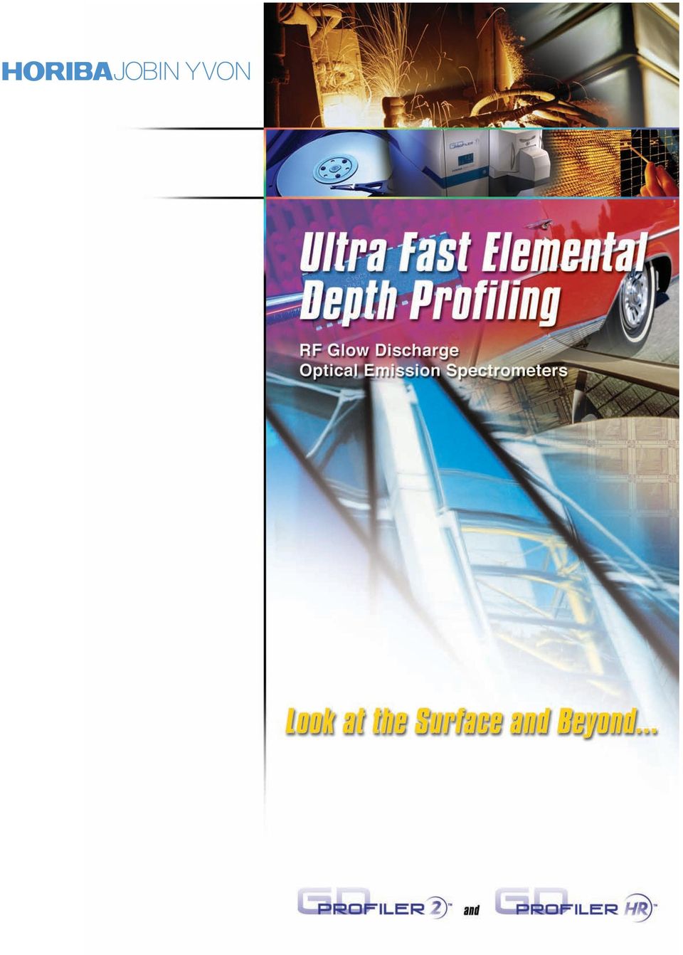
2 GD-Profiler Series RF Glow Discharge Optical Emission Spectrometers For many applications, it is essential to know the chemical composition of a material, both at the surface, at the interfaces and in the bulk. Whether the application is coated steels, e.g. for car bodies, or semiconductor wafers, e.g. for integrated circuit manufacture, the surface composition determines many important parameters such as appearance, corrosion resistance, adhesion, conductivity, etc, while the bulk composition is important for the stability and long life of the product. Only one technique, RF Glow Discharge Optical Emission Spectrometry (RF-GD-OES) can provide both the surface and bulk composition, quickly, inexpensively, and with high sensitivity to all elements (including the gaseous elements), for almost all solid materials, including metals, metal alloy coatings, semiconductors, polymer coatings, glass, ceramics, etc. The GD-Profilers use a Class E RF generator optimized for stability and crater shape allowing for real surface analysis. This is due to the RF source's constant MHz frequency and the rapid response of the matching box. Since the source can be pulsed at a millisecond rate, very fragile samples may be analyzed. HORIBA Jobin Yvon (HJY) original, ion-etched holographic gratings assure the highest light throughput for maximum light efficiency and sensitivity. High-performance, patented High Dynamic Detectors (HDD ) provide speed and sensitivity in detection without compromise a dynamic range of with microsecond speed. Easily accessible sample compartments allow plenty of room for sample loading, even with large samples. Accessories for small samples or non-flat samples are available. The patented CenterLite Laser Alignment System provides for precise sample positioning. View of the GD-Profiler 2 The GD-Profiler 2 s simultaneous 0.5m polychromator allows the determination of up to 47 elements between 110 and 800nm. This allows the determination of H, O, C, N, and Cl and it also gives an optical resolution between 18 and 25 pm for all elements. RF GD Depth Profile revealing a gold layer on NiP on brass and the GD spot on the sample after analysis. Total measurement time: 2 minutes. (Courtesy of EMPA Switzerland) The monochromator option, available only from HJY, provides the perfect tool to increase instrument flexibility by allowing any element to be added to the analytical program(`n+1 ). Elemental analysis from the first nanometer down to more than 150 microns The GD-Profiler Series of RF-GD-OES offers two models, each with a variety of options to suit an extensive range of applications. The GD-Profiler 2 is a very compact instrument with high flexibility, while the GD-Profiler HR offers unmatched performance with its ultra high resolution optics. The monochromator also allows full spectrum acquisition in as little as two minutes. Thus a complete sample fingerprint is available which can be examined with HJY's unique IMAGE software. The GD-Profiler HR offers 1.0m focal length providing optical resolution of 14pm with the simultaneous analysis of up to 60 channels. The optional 1.0m monochromator of the GD-Profiler HR offers the highest optical resolution available of 9pm in the UV. View of the GD-Profiler HR with ultra high resolution combined optics 2 3

3 Bulk, Surface and Depth Profiling, Conductive and non Conductive GD-Profiler Series RF-GD-OES system combines a glow discharge powered by a radio frequency (RF) source with an optical emission spectrometer. The essence of a glow discharge instrument is the source which supplies power to create the GD plasma. The HJY design allies the advantages of the Grimm lamp design featuring a dual pumping system with the RF Marcus lamp where RF is applied to the sample and not to a cathode block. Typical 2-D crater obtained on Zn coated steel. The double pumping system of the HJY RF lamp minimizes the redeposition on the edges of the crater. This allows analysis down to 150 microns with excellent flatness, which is critical for depth resolution. The technique is now internationally recognized (ISO on the analysis of Zn and Al coatings). The spacious sample compartment provides room for a variety of sample sizes and provides ease in sample mounting due to the primary vacuum and CenterLite laser pointer mounted on the automatic cleaning reamer behind the sample. Separation of the sputtering and light emission area minimizes matrix effects, providing linear calibration curves and allows for the mixing of various alloys in one analytical program. Cooling of the sample with a recirculating water system allows temperatures close to zero degrees Celsius, making it possible for the analysis of thin films, such as polymers, which may melt at higher temperatures. Hard coatings are of major commercial interest and are commonly prepared by chemical vapor deposition (CVD) or physical vapor deposition (PVD). RF-GD-OES has much to offer to this industry by assisting in the development of new products and in quality assurance and production problem solving. The GD-Profiler series of instruments offers the perfect solution for these types of samples, which are multi-layered, complex coatings. The above depth profile shows the analysis of 25 layers of AlN/TiN (20nm each) deposited on Si. Benefit of the pulse source and synchronized acquisition. Application to thin layers on a fragile glass. Analysis of all elements including C, H, O, N, Cl, F. Vacuum inlets Stainless steel source body Photons on their way to OES Low argon consumption of less than 0.3 L/minute minimizes the cost of analysis. The pulsable RF design allows the rapid analysis of both conductive and non-conductive layers or materials. Built in Metal Maker provides ultra fast charge calculation and correction, an essential tool in the metal industry. Full emission spectrum record with comparison to the library of lines. 4 Copper anode with tube Collar & ceramic Sample RF applicator and closed loop cooling block Argon gas inlet Although ideal samples for GD are flat and large enough to cover the source O-ring, the need for only a primary vacuum allows the analysis of small or irregularly shaped samples through the use of special sample holders. Even coated wires have been successfully characterized. By attaching a DC Arc Source to the optical system, the trace analysis of powders is possible. The Time Resolved Measurement of the GD Profiler is ideally suitable for DC arc type analysis. Crater on a screw head using the universal sample holder attachment GD-PROFILER Points RF-GD provides the ability to perform the same types of bulk, elemental analysis as traditional OE systems (arc/spark) with a typical precision of 0.4% for the main elements and an analysis time of about 90 seconds HJY provides calibrations for both bulk and compositional depth profile (CDP) for alloys of Fe, Al, Cu, Ti, Ni, Co, Zn, Sn and Pb using Certified Reference Materials. Custom calibrations are also available The pulse mode s soft sputtering allows analysis of fragile materials (layers on glass, etc). Acquisition is synchronized with the pulses for optimum detection. Full spectrum of a sample featuring molecular bands that could affect the reading of elements at certain wavelengths. The GD-Profiler Series offers a world of applications opportunities for thin films, PVD/CVD coatings, coated steels, oxidation/corrosion/passivation, surface treatments, semiconductors, metal alloys, ceramics, powders, and glasses HJY sample holders allow for the analysis of all sample shapes including tubes, rods, rough surfaces, etc. ISO Technical Committee TC 201 recognizes RF Glow Discharge as a valid technique for depth profile analysis 5

4 Speed and Sensitivity without Compromise for any Application Depth profile analysis is a continuous process of sputtering through a sample at a rate of typically 3 microns per minute. At such a speed, two parameters are critical. First and foremost is time. Valuable information is lost with any time spent waiting or integrating. Second is the ability to respond accurately and immediately to the rapidly changing concentrations as you work through different layers and arrive at various interfaces. This means the ability to measure elements at both trace and major concentrations instantaneously. The same element, which may be at a trace level in one layer, could become a major component in another layer. This type of analysis demands a detection system that has high sensitivity for low intensity levels without using long integration times. It also requires an optical design and electronic acquisition system that can acquire a large quantity of information very rapidly. The main polychromator of the GD-Profiler instruments provide coverage from 110 to 620 nm. The optic offers a direct view of the plasma without the use of fiber optics, maximizing the efficiency in the UV. Ion-etched holographic gratings and few reflective surfaces mean maximum light throughput and efficiency for excellent detection limits. A nitrogen purge is used for low UV analysis. The enhanced resolution of the GD-Profiler HR provides the performance required for more difficult sample types and applications. HJY developed and patented the High Dynamic Detection (HDD) system. This unique design offers speed and sensitivity in detection without compromise. Because it utilizes a PMT, it offers unsurpassed detection capability for trace elements using short integration times, allowing the instrument to acquire more critical information at the surface and in the first seconds of sputtering or at the interfaces. The HDD design also extends the linear dynamic range of acquisition to 10 10, thus allowing the instrument to respond to signals at the interface varying from low counts to millions in the millisecond timeframe without saturation or voltage preadjustment. This response cannot be achieved with fixed high voltage systems or solid state detectors. With the IMAGE feature, the GD-Profiler instruments can also perform full spectrum fingerprinting of your sample or layer using the automatic HDD detection system and ultra fast acquisition electronics. The flat field option extends the wavelength range to 800 nm to include Li, K, F and Cs. HJY was the first to design and patent the flat field in This unique design utilizes the primary optical beam directed to a second 1200 groove/mm grating. HJY offers the unique ability to extend the flexibility of your GD-Profiler instrument by adding a monochromator. The simultaneous n+1 analysis during depth profiling is critical in research, where being able to determine an element not on the polychromator can be most useful. The mono option also offers improved resolution compared to the poly, which is beneficial for trace element or molecular band observation. The Image software is provided with the monochromator. It allows spectrum fingerprinting of a sample or a thick layer in less than 2 minutes. V Cr Fe In addition to the poly, flat field and mono a fast CCD system could be added to the GD-Profiler and used in complement of the flat field to provide simultaneous measurements of some extra lines (essentially in the IR region for alcali elements and Ar lines). However by nature such CCD components have limited dynamics and are not fast enough for ultra thin layers. Detailed view of the GD-Profiler B Mg sec GD-PROFILER Points 6 Complex coating on steel with HDD and without HDD. Without HDD the dynamic range is limited to 10V leading to saturation of the Cr signal in the coating (and partly of the B one) and of the Fe signal in the substrate. HDD mode is extensively used for calibration, bulk and surface analysis. The HJY gratings provide highest light throughput HJY offers various optical combinations for maximum spectral coverage and flexibility. The monochromator option is a feature unique to HJY and not found on any other commercially available GD All GD-Profiler instruments offer patented HDD detection resulting in automatic high voltage adjustment HDD is perfect for small, unknown samples where only one spot can be made, as it provides a tailored acquisition for accurate analysis IMAGE provides a great tool for semi-quantitative analysis, method development and sample archiving 7

5 Quantum XP, Information and Technology in a Software Quantum XP is a comprehensive multitasking management tool for the GD-Profiler Series allowing bulk and surface analysis in one package. It is loaded with features like IQ, Intelligent Quantification, that takes the mystery out of the math behind producing accurate Compositional Depth Profiles, TimePlus that allows one to increase the measurement time during a depth profile acquisition and the powerful Quantum Tabler that organizes your valuable data and presents them in easily customizable formats. Two mechanisms yield a powerful technique. 1) In RF GD-OES the material is efficiently sputtered by Ar ions. This first process is material dependent (i.e. the sputtering efficiency depends on the structure and the composition of the material). 2) The ejected atoms navigate in the plasma which is located above the sample surface but away from the surface. They can be considered as free atoms. The light they produce is therefore only dependent on their number and of the plasma characteristics but not anymore on the sample itself so samples from different materials can be calibrated together, provided we know their sputtering efficiency. This light can then be measured and quantified by the optical spectrometer. Bulk analysis window Combining the two processes it is therefore possible to derive the composition and the sputtering efficiency of a multilayer system simply from the recorded light intensities after proper calibration of the instrument. Surface analysis. Multiple windows showing qualitative and quantitative analysis of a treated steel with 3D display. Time Plus function to increase analysis time during measurement Estimation of trends IQ Intelligent Quantification for Compositional Quantitative Depth Profiles Integrated libraries of reference materials, optical wavelengths and sputtering rates Multilingual software Flexible definition of tasks for repetitive work 3D display Powerful and flexible data handling Multitasking allows one to check calibration curves in parallel with the study of a single or multi surface result or to prepare reports while measuring a sample. 8 Comparison of Carbon and Nitrogen depth profiles on different treated steels and calibration curve of Carbon in CDP mode. An inside look at the principles of Glow Discharge and what is happening in the anode anode allows us to understand why RF-GD-OES is a truly quantitative technique. A double mechanism is in process. The Intelligent Quantification (IQ) takes full benefit of the knowledge of RF Glow Discharge to provide Compositional Quantitative Depth Profiles from the qualitative information recorded 9
 In RF GD-OES the material is efficiently sputtered by Ar ions. This first process is material dependent (i.e. the sputtering efficiency depends on the structure and the composition of the material).")
6 RF Glow Discharge Optical Emission Spectrometry for Surface and Thin Film Analysis The capability of RF-GD-OES as a tool in surface science is now recognized. Though the technique does not provide lateral resolution, its speed and its ease of use make it the technique of choice for many investigations. Recent examples on hard disks, PZT layers, multilayers on glasses and thin oxides on metals have been published widely. For all these applications, the low energy of the incident particles in RF GD (50eV) assures minimal surface damage. The speed of RF-GD-OES allows depth profiles of both thin and thick films. The typical sputtering rate in RF-GD-OES is nm per second representing atomic layers per second, but since the counting rates of the patented High Dynamic Detectors (HDD) are very fast the instrument is routinely capable of making 1-10 measurements per element per atomic layer. 7nm O 3+ AI Cr 3 + PO AI Intensity (a.u.) Cr 7nm Al Distance from oxide surface (nm) GD result Intensity (a.u.) Cr 7nm 0 50 Distance from oxide surface (nm) SIMS result Anodic oxidation of aluminum films in appropriate electrolytes leads to the formation of thin (<1um) barrier anodic oxide films. The top left schematic shows such a film after anodizing in a sodium chromate solution. A comparison of the GD-OES analysis and that of secondary ion mass spectrometry (SIMS) was made for this sample. The distribution of chromium in the film compares well between the two techniques, however, the time of analysis was quite different. In GD-OES the time to reach the metal/oxide interface was 9 seconds, as compared to 60 minutes to reach this interface with SIMS. Recent outstanding results have been published showing the capability of RF-GD-OES to depth resolve some molecules deposited on Cu. This is evidence of the resolution of the technique. The analysis of commercial hard disks is a challenge for most surface techniques, due to the large variations in thickness throughout the layers of the disks. The fullscale depth profile above shows the ability of GD-OES to sputter through the 12 m amorphous Ni-P layer to the Al-Mg substrate in less than 200 seconds (sampling time 0.1 seconds). The transmission electron micrograph images of an ultramicrotomed section of the hard disk confirm the presence of these layers on the disk substrate. At the right, shown in (a), a general view at low magnification. JY RECEIVED THE PRESTIGIOUS NASA EXCELLENCE AWARD Over 180 years of JY optical experience provides the platform for NASA projects. This same quality is at the heart of every GD-PROFILER Series instrument. GD-PROFILER Points Analysis times are typically 100 times faster than classical surface techniques that operate in UHV environment. Sensitivity of RF-GD is in the range of atoms/cm 2 Non conductors can be analyzed with RF GD without surface charging effects All elements can be measured in one shot (including H, O, Cl) Depth Resolution is in the nm range GD is complimentary to other techniques that provide imaging, lateral resolution or molecular information A zoom of the near-surface region above (left) reveals the lubricant layer, diamond-like carbon protective layer, and the cobalt-chromium 10 magnetic alloy and chromium layers, each approximately 20-30nm thick, which were successively deposited over the disks. Sampling time of the near-surface region was 0.01 seconds. The image in (b) is a high magnification view of the area in the red box at the top of (a) above. All data used with the permission of its authors and publishers. 11
 assures minimal surface damage. The speed of RF-GD-OES allows depth profiles of both thin and thick films.")
7 Discover A Whole New World of Support We know Glow Discharge and its multiple application possibilities and we know that you need a dedicated solution. Our staff of analytical specialists, advice from world-recognized experts in GD, provision of reference materials, a comprehensive data base of publications and links to other users around the world provide the tools necessary to achieve results. Training programs that balance theory with practical hands-on experience World wide Applications assistance ALLIANCE on line catalog of supplies, accessories and upgrades Comprehensive partnership agreements for service maintenance User Group meetings and World Link Network provide continuous communication ISO 9001:2000 Certificate No 1995/4751 Your local representative Specifications and instrument appearance subject to change without notice. info@jobinyvon.fr France: HORIBA Jobin Yvon S.A.S., 16-18, rue du Canal, Longjumeau Cedex, Tel: +33 (0) , Fax: +33 (0) , USA: HORIBA Jobin Yvon Inc., 3880 Park Avenue, Edison, NJ , Toll-Free: jobinyvon Tel: , Fax: , info@jobinyvon.com, Japan: HORIBA Ltd., JY Optical Sales Dept, Higashi-Kanda, Daiji Building, Higashi-Kanda Chiyoda-ku, Tokyo , Tel: +81 (0) , Germany: +49 (0) Italy: UK: +44 (0) China: +86 (0)

Analysis of Chlorine, Bromine and Iodine in Water using ICP-AES
 ICP OPTICAL ATOMIC EMISSION SPECTROSCOPY Analysis of Chlorine, Bromine and Iodine in Water using ICP-AES HORIBA Scientific Longjumeau, France Keywords: metallurgy, non-ferrous, halogens 1 Introduction
h e l p s y o u C O N T R O L
 contamination analysis for compound semiconductors ANALYTICAL SERVICES B u r i e d d e f e c t s, E v a n s A n a l y t i c a l g r o u p h e l p s y o u C O N T R O L C O N T A M I N A T I O N Contamination
Quality Assurance for the Analysis of Steel by Gas Component Analysis
 Quality Assurance for the Analysis of Steel by Gas Component Analysis Alain Salaville, Jérôme Barraqué, JOBIN YVON SAS, Longjumeau, FRANCE Keywords: quality assurance, steel 1 Overview Quality assurance
Ion Beam Sputtering: Practical Applications to Electron Microscopy
 Ion Beam Sputtering: Practical Applications to Electron Microscopy Applications Laboratory Report Introduction Electron microscope specimens, both scanning (SEM) and transmission (TEM), often require a
2015 Training Courses
 2015 Training Courses GDS, ICP-OES, Particle Size Analysis, C/S & O/N/H, S & Cl in Petroleum, X-Ray Fluorescence Exceeding Customer Expectations Training courses calendar 2015 HORIBA Scientific offers
Coating Technology: Evaporation Vs Sputtering
 Satisloh Italy S.r.l. Coating Technology: Evaporation Vs Sputtering Gianni Monaco, PhD R&D project manager, Satisloh Italy 04.04.2016 V1 The aim of this document is to provide basic technical information
Nano-Spectroscopy. Solutions AFM-Raman, TERS, NSOM Chemical imaging at the nanoscale
 Nano-Spectroscopy Solutions AFM-Raman, TERS, NSOM Chemical imaging at the nanoscale Since its introduction in the early 80 s, Scanning Probe Microscopy (SPM) has quickly made nanoscale imaging an affordable
Secondary Ion Mass Spectrometry
 Secondary Ion Mass Spectrometry A PRACTICAL HANDBOOK FOR DEPTH PROFILING AND BULK IMPURITY ANALYSIS R. G. Wilson Hughes Research Laboratories Malibu, California F. A. Stevie AT&T Bell Laboratories Allentown,
Neuere Entwicklungen zur Herstellung optischer Schichten durch reaktive. Wolfgang Hentsch, Dr. Reinhard Fendler. FHR Anlagenbau GmbH
 Neuere Entwicklungen zur Herstellung optischer Schichten durch reaktive Sputtertechnologien Wolfgang Hentsch, Dr. Reinhard Fendler FHR Anlagenbau GmbH Germany Contents: 1. FHR Anlagenbau GmbH in Brief
Adapter Catalog MOBILE METAL ANALYZER. SPECTRO isort and SPECTROTEST
 Adapter Catalog MOBILE METAL ANALYZER SPECTRO isort and SPECTROTEST Testing Adapters for Mobile Metal Analyzers A full range of metal analyzer products for onsite metal analysis tasks SPECTRO isort SPECTROTEST
Ultima Expert Ultimate ICP-OES Spectrometer Best Performance & Ease-of-Use
 Ultima Expert Ultimate ICP-OES Spectrometer Best Performance & Ease-of-Use Designed to Handle the Most Challenging Applications HORIBA Scientific develops and manufactures high performance ICP-OES spectrometers
Vacuum Evaporation Recap
 Sputtering Vacuum Evaporation Recap Use high temperatures at high vacuum to evaporate (eject) atoms or molecules off a material surface. Use ballistic flow to transport them to a substrate and deposit.
2. Deposition process
 Properties of optical thin films produced by reactive low voltage ion plating (RLVIP) Antje Hallbauer Thin Film Technology Institute of Ion Physics & Applied Physics University of Innsbruck Investigations
Multi-elemental determination of gasoline using Agilent 5100 ICP-OES with oxygen injection and a temperature controlled spray chamber
 Multi-elemental determination of gasoline using Agilent 5100 ICP-OES with oxygen injection and a temperature controlled spray chamber Application note Energy & chemicals, petrochemicals Authors Elizabeth
THIN FILM MATERIALS TECHNOLOGY
 THIN FILM MATERIALS TECHNOLOGY Sputtering of Compound Materials by Kiyotaka Wasa Yokohama City University Yokohama, Japan Makoto Kitabatake Matsushita Electric Industrial Co., Ltd. Kyoto, Japan Hideaki
For Touch Panel and LCD Sputtering/PECVD/ Wet Processing
 production Systems For Touch Panel and LCD Sputtering/PECVD/ Wet Processing Pilot and Production Systems Process Solutions with over 20 Years of Know-how Process Technology at a Glance for Touch Panel,
Simplicity. Reliability. Performance
 Simplicity Reliability Performance ICP Without Compromise At Teledyne Leeman Labs atomic spectroscopy is our business, our only business. We are deeply committed to providing you with technically superior
Anodes and Misc Equipment
 Anodes and Misc Equipment Application: Platinised Titanium Anodes Platinised titanium anodes are recommended for use in the following electrolytic processes:- Precious metal electroplating - e.g. Au, Pt,
The photoionization detector (PID) utilizes ultraviolet
 utilizes ultraviolet") Chapter 6 Photoionization Detectors The photoionization detector (PID) utilizes ultraviolet light to ionize gas molecules, and is commonly employed in the detection of volatile organic compounds (VOCs).
Chapter 6 Photoionization Detectors The photoionization detector (PID) utilizes ultraviolet light to ionize gas molecules, and is commonly employed in the detection of volatile organic compounds (VOCs).
High Rate Oxide Deposition onto Web by Reactive Sputtering from Rotatable Magnetrons
 High Rate Oxide Deposition onto Web by Reactive Sputtering from Rotatable Magnetrons D.Monaghan, V. Bellido-Gonzalez, M. Audronis. B. Daniel Gencoa, Physics Rd, Liverpool, L24 9HP, UK. www.gencoa.com,
A Remote Plasma Sputter Process for High Rate Web Coating of Low Temperature Plastic Film with High Quality Thin Film Metals and Insulators
 A Remote Plasma Sputter Process for High Rate Web Coating of Low Temperature Plastic Film with High Quality Thin Film Metals and Insulators Dr Peter Hockley and Professor Mike Thwaites, Plasma Quest Limited
Spectral Measurement Solutions for Industry and Research
 Spectral Measurement Solutions for Industry and Research Hamamatsu Photonics offers a comprehensive range of products for spectroscopic applications, covering the, Visible and Infrared regions for Industrial,
Coating Thickness and Composition Analysis by Micro-EDXRF
 Application Note: XRF Coating Thickness and Composition Analysis by Micro-EDXRF www.edax.com Coating Thickness and Composition Analysis by Micro-EDXRF Introduction: The use of coatings in the modern manufacturing
Lecture 12. Physical Vapor Deposition: Evaporation and Sputtering Reading: Chapter 12. ECE 6450 - Dr. Alan Doolittle
 Lecture 12 Physical Vapor Deposition: Evaporation and Sputtering Reading: Chapter 12 Evaporation and Sputtering (Metalization) Evaporation For all devices, there is a need to go from semiconductor to metal.
OLED - Technologie der Zukunft
 OLED - Technologie der Zukunft Dr. Manfred Weigand MERCK KGaA, Darmstadt, Germany Cleanzone 2014 Cathode Ray Tube (CRT) Source: Peter Littmann Source: Patrick Schindler Source: Bundesarchiv, Bild 183-H0812-0031-001
Pore size and BET surface area. analysis at your fingertips. SA 3100. Gas Adsorption Analyzer
 Pore size and BET surface area analysis at your fingertips. SA 3100 Gas Adsorption Analyzer The History of Beckman Coulter Particle Characterization Introducing The SA 3100 Surface Area and Pore Size Analyzer
Scanning Electron Microscopy Services for Pharmaceutical Manufacturers
 Scanning Electron Microscopy Services for Pharmaceutical Manufacturers Author: Gary Brake, Marketing Manager Date: August 1, 2013 Analytical Testing Laboratory www.atl.semtechsolutions.com Scanning Electron
AMD Analysis & Technology AG
 AMD Analysis & Technology AG Application Note 120419 Author: Karl-Heinz Maurer APCI-MS Trace Analysis of volatile organic compounds in ambient air A) Introduction Trace analysis of volatile organic compounds
Tableting Punch Performance Can Be Improved With Precision Coatings
 Tableting Punch Performance Can Be Improved With Precision Coatings by Arnold H. Deutchman, Ph. D. Director of Research and Development (614) 873-4529 X 114 adeutchman@beamalloy.net Mr. Dale C. Natoli
Lapping and Polishing Basics
 Lapping and Polishing Basics Applications Laboratory Report 54 Lapping and Polishing 1.0: Introduction Lapping and polishing is a process by which material is precisely removed from a workpiece (or specimen)
How To Analyze Plasma With An Inductively Coupled Plasma Mass Spectrometer
 What is ICP-MS? and more importantly, what can it do? Inductively Coupled Plasma Mass Spectrometry or ICP-MS is an analytical technique used for elemental determinations. The technique was commercially
LabRAM HR. Research Raman Made Easy! Raman Spectroscopy Systems. Spectroscopy Suite. Powered by:
 LabRAM HR Research Raman Made Easy! Raman Spectroscopy Systems Powered by: Spectroscopy Suite Cutting-Edge Applications with the LabRAM HR Deeply involved in Raman spectroscopy for decades, HORIBA Scientific
View of ΣIGMA TM (Ref. 1)
") Overview of the FESEM system 1. Electron optical column 2. Specimen chamber 3. EDS detector [Electron Dispersive Spectroscopy] 4. Monitors 5. BSD (Back scatter detector) 6. Personal Computer 7. ON/STANDBY/OFF
Overview of the FESEM system 1. Electron optical column 2. Specimen chamber 3. EDS detector [Electron Dispersive Spectroscopy] 4. Monitors 5. BSD (Back scatter detector) 6. Personal Computer 7. ON/STANDBY/OFF
NANOCOMPOSIX'S GUIDE TO ICP-MS MEASUREMENT
 NANOCOMPOSIX'S GUIDE TO ICP-MS MEASUREMENT AND ANALYSIS SEPTEMBER 2012, V 1.1 4878 RONSON CT STE K SAN DIEGO, CA 92111 858-565 - 4227 NANOCOMPOSIX.COM Note to the Reader: We at nanocomposix have published
FRAUNHOFER INSTITUTe For
 FRAUNHOFER INSTITUTe For surface engineering and thin films MOCCA + PROCESS AUTOMATION & OPTICAL MONITORING MOCCA + Automate your thin film coating process In many thin film coating processes various factors
In-line 3D Sputtering Coating System. Fully automated. pst line
 In-line 3D Sputtering Coating System Fully automated pst line pst line In-line 3D Sputtering Coating System Fully in-line automated base coat, 3D sputtering and top coat system Ultra efficient varnishing
THERMO NORAN SYSTEM SIX ENERGY DISPERSIVE X- RAY SPECTROMETER. Insert Nickname Here. Operating Instructions
 THERMO NORAN SYSTEM SIX ENERGY DISPERSIVE X- RAY SPECTROMETER Insert Nickname Here Operating Instructions Table of Contents 1 INTRODUCTION Safety 1 Samples 1 2 BACKGROUND Background Information 3 References
pst line Fully automated In-line 3D Sputtering Coating System The right choice
 pst line In-line 3D Sputtering Coating System Fully automated The right choice a new standard in sputtering technology pst line In-line 3D Sputtering Coating System loading & off-loading substrate cleaning
High-end stationary vacuum spectrometer. Innovation with Integrity OES
 Q8 MAGELLAN High-end stationary vacuum spectrometer Innovation with Integrity OES The Evolution of Perfection Engineered for ultimate sparc spectrometry Next Step to perfection The genes are right: Q8
Reactive Sputtering Using a Dual-Anode Magnetron System
 Reactive Sputtering Using a Dual-Anode Magnetron System A. Belkind and Z. Zhao, Stevens Institute of Technology, Hoboken, NJ; and D. Carter, G. McDonough, G. Roche, and R. Scholl, Advanced Energy Industries,
Machbarkeitsstudie zu geeigneten Kandidaten für f r die Herstellung von CRM für r die Bestimmung von Wasserstoff in Festkörpern
 BAM mission: Safety in technology and chemistry Machbarkeitsstudie zu geeigneten Kandidaten für f r die erstellung von CRM für r die Bestimmung von Wasserstoff in Festkörpern V.-D. odoroaba, a D. Klemm,
QGA Quantitative Gas Analyser
 QGA Quantitative Gas Analyser A compact bench-top system for real-time gas and vapour analysis Detailed product information / introduction catalysis studies environmental gas analysis fermentation off-gas
RoHS Test Methods. Presented by: Bruce Peterson
 RoHS Test Methods Presented by: Bruce Peterson Motivation for Presentation The EU RoHS directive takes effect July 1, 2006 Customer confusion about - Scope of directive How much testing needs to be performed
Basic Properties and Application of Auto Enamels
 Basic Properties and Application of Auto Enamels Composition of Ceramic Automotive Glass Enamels Ceramic automotive glass colours are glass enamels that fire on to the glass during the bending process
Lecture 9. Surface Treatment, Coating, Cleaning
 1 Lecture 9. Surface Treatment, Coating, Cleaning These processes are sometimes referred to as post-processing. They play a very important role in the appearance, function and life of the product. Broadly,
Lasers Design and Laser Systems
 Lasers Design and Laser Systems Tel: 04-8563674 Nir Dahan Tel: 04-8292151 nirdahan@tx.technion.ac.il Thank You 1 Example isn't another way to teach, it is the only way to teach. -- Albert Einstein Course
Modern approaches to determination of toxic metals in marine environmental objects. Atomic absorption and inductively coupled plasma, advantages and
 Modern approaches to determination of toxic metals in marine environmental objects. Atomic absorption and inductively coupled plasma, advantages and disadvantages Atomic spectroscopy Atomic spectroscopy
Electron Microscopy 3. SEM. Image formation, detection, resolution, signal to noise ratio, interaction volume, contrasts
 Electron Microscopy 3. SEM Image formation, detection, resolution, signal to noise ratio, interaction volume, contrasts 3-1 SEM is easy! Just focus and shoot "Photo"!!! Please comment this picture... Any
Spectroscopy. Biogeochemical Methods OCN 633. Rebecca Briggs
 Spectroscopy Biogeochemical Methods OCN 633 Rebecca Briggs Definitions of Spectrometry Defined by the method used to prepare the sample 1. Optical spectrometry Elements are converted to gaseous atoms or
University of Wisconsin Chemistry 524 Spectroscopic Applications (GFAA, ICP, UV/Vis, Fluorescence)
") University of Wisconsin Chemistry 524 Spectroscopic Applications (GFAA, ICP, UV/Vis, Fluorescence) For this laboratory exercise, you will explore a variety of spectroscopic methods used in an analytical
University of Wisconsin Chemistry 524 Spectroscopic Applications (GFAA, ICP, UV/Vis, Fluorescence) For this laboratory exercise, you will explore a variety of spectroscopic methods used in an analytical
Modular Glovebox Systems Gas Purifier Units Antechambers Accessories
 Modular Glovebox Systems Gas Purifier Units Antechambers Accessories INERTGAS TECHNOLOGY Modular glovebox with screwed in flanged side panels Easy to extend or modify while keeping a flat work place Define
X-RAY FLUORESCENCE SPECTROSCOPY IN PLASTICS RECYCLING
 X-RAY FLUORESCENCE SPECTROSCOPY IN PLASTICS RECYCLING Brian L. Riise and Michael B. Biddle MBA Polymers, Inc., Richmond, CA, USA Michael M. Fisher American Plastics Council, Arlington, VA, USA X-Ray Fluorescence
Application Note AN1
 TAKING INVENTIVE STEPS IN INFRARED. MINIATURE INFRARED GAS SENSORS GOLD SERIES UK Patent App. No. 799A USA Patent App. No. 9/78,7 World Patents Pending SENSOR OVERVIEW Application Note AN The Dynament
13C NMR Spectroscopy
 13 C NMR Spectroscopy Introduction Nuclear magnetic resonance spectroscopy (NMR) is the most powerful tool available for structural determination. A nucleus with an odd number of protons, an odd number
The best lab standard. 1,4 Megapixels 2/3 inch sensor Giant pixel size 6 times optical zoom Massive 16-bit imaging for enhanced dynamic
 1 AGENDA Product roadmap...3 Computer based system: PLATINUM..5 XPLORER.6 ESSENTIAL..7 Specifications Computer based system..8 Configuration Computer based system... 9 Software Computer based system...10
Determination of Metals in a 3% Sodium Chloride (NaCl) Matrix by Axially-Viewed ICP-OES
 Matrix by Axially-Viewed ICP-OES") Determination of Metals in a 3% Sodium Chloride (NaCl) Matrix by Axially-Viewed ICP-OES Application Note Inductively Coupled Plasma-Optical Emission Spectrometers Author Deen Johnson Introduction The development
Determination of Metals in a 3% Sodium Chloride (NaCl) Matrix by Axially-Viewed ICP-OES Application Note Inductively Coupled Plasma-Optical Emission Spectrometers Author Deen Johnson Introduction The development
How compact discs are made
 How compact discs are made Explained by a layman for the laymen By Kevin McCormick For Science project at the Mountain View Los Altos High School Abstract As the major media for music distribution for
Agilent Cary 4000/5000/6000i Series UV-Vis-NIR
 Agilent Cary 4000/5000/6000i Series UV-Vis-NIR Guaranteed specifications Design overview Double beam, ratio recording, double out-of-plane Littrow monochromator UV-Vis-NIR spectrophotometer (Agilent Cary
Short overview of TEUFEL-project
 Short overview of TEUFEL-project ELAN-meeting may 2004 Frascati (I) Contents Overview of TEUFEL project at Twente Photo cathode research Recent experience Outlook Overview FEL Drive laser Photo cathode
Application of Automated Data Collection to Surface-Enhanced Raman Scattering (SERS)
") Application Note: 52020 Application of Automated Data Collection to Surface-Enhanced Raman Scattering (SERS) Timothy O. Deschaines, Ph.D., Thermo Fisher Scientific, Madison, WI, USA Key Words Array Automation
Application Note: 52020 Application of Automated Data Collection to Surface-Enhanced Raman Scattering (SERS) Timothy O. Deschaines, Ph.D., Thermo Fisher Scientific, Madison, WI, USA Key Words Array Automation
Using Direct Solid Sampling ICP-MS to Complement SEM- EDX and SIMS in Characterizing Semiconductor Materials
 Using Direct Solid Sampling ICP-MS to Complement SEM- EDX and SIMS in Characterizing Semiconductor Materials Fuhe Li and Scott Anderson Air Liquide America-Balazs Analytical Services, 4649 Landing Parkway,
Lecture 6 Scanning Tunneling Microscopy (STM) General components of STM; Tunneling current; Feedback system; Tip --- the probe.
 General components of STM; Tunneling current; Feedback system; Tip --- the probe.") Lecture 6 Scanning Tunneling Microscopy (STM) General components of STM; Tunneling current; Feedback system; Tip --- the probe. Brief Overview of STM Inventors of STM The Nobel Prize in Physics 1986 Nobel
Lecture 6 Scanning Tunneling Microscopy (STM) General components of STM; Tunneling current; Feedback system; Tip --- the probe. Brief Overview of STM Inventors of STM The Nobel Prize in Physics 1986 Nobel
Atomic Structure. Atoms consist of: Nucleus: Electrons Atom is electrically balanced equal electrons and protons. Protons Neutrons
 Basics of Corrosion Performance Metals Sacrificial anode manufacturer Specialize in aluminum alloy anodes All products made in the USA (Berks county, PA) ISO9001/2001 Certified Quality System Also traditional
Laboratory #3 Guide: Optical and Electrical Properties of Transparent Conductors -- September 23, 2014
 Laboratory #3 Guide: Optical and Electrical Properties of Transparent Conductors -- September 23, 2014 Introduction Following our previous lab exercises, you now have the skills and understanding to control
The Basics of Scanning Electron Microscopy
 The Basics of Scanning Electron Microscopy The small scanning electron microscope is easy to use because almost every variable is pre-set: the acceleration voltage is always 15kV, it has only a single
Heat Treatment Process
 Heat Treatment Process Holytown, Scotland UK Resistors - Insulation - Protection Chongqing, China C/C fixturing, rods & beams Insulation St-Marys, USA Gennevilliers, France Main production sites Industrial
Nanoscale Resolution Options for Optical Localization Techniques. C. Boit TU Berlin Chair of Semiconductor Devices
 berlin Nanoscale Resolution Options for Optical Localization Techniques C. Boit TU Berlin Chair of Semiconductor Devices EUFANET Workshop on Optical Localization Techniques Toulouse, Jan 26, 2009 Jan 26,
Experiment #5: Qualitative Absorption Spectroscopy
 Experiment #5: Qualitative Absorption Spectroscopy One of the most important areas in the field of analytical chemistry is that of spectroscopy. In general terms, spectroscopy deals with the interactions
Chapter 4 COATINGS Full Reflective Coatings:
 Chapter 4 COATINGS Technical developments in coatings for plastic optics have resulted in optical and durability characteristics once believed possible only with glass. These advances in coating technology
Quality Control on Aerospace Components Using Handheld X-ray Fluorescence (XRF)
") International Workshop SMART MATERIALS, STRUCTURES & NDT in AEROSPACE Conference NDT in Canada 2011 2-4 November 2011, Montreal, Quebec, Canada Quality Control on Aerospace Components Using Handheld X-ray
International Workshop SMART MATERIALS, STRUCTURES & NDT in AEROSPACE Conference NDT in Canada 2011 2-4 November 2011, Montreal, Quebec, Canada Quality Control on Aerospace Components Using Handheld X-ray
3. What would you predict for the intensity and binding energy for the 3p orbital for that of sulfur?
 PSI AP Chemistry Periodic Trends MC Review Name Periodic Law and the Quantum Model Use the PES spectrum of Phosphorus below to answer questions 1-3. 1. Which peak corresponds to the 1s orbital? (A) 1.06
Single Mode Fiber Lasers
 Single Mode Fiber Lasers for Industrial and Scientific Applications T h e P o w e r t o T r a n s f o r m T M IPG s Single Mode Fiber Lasers Advantages IPG's YLR-SM Series represents a break-through generation
Conductivity of silicon can be changed several orders of magnitude by introducing impurity atoms in silicon crystal lattice.
 CMOS Processing Technology Silicon: a semiconductor with resistance between that of conductor and an insulator. Conductivity of silicon can be changed several orders of magnitude by introducing impurity
PHYSICAL METHODS, INSTRUMENTS AND MEASUREMENTS Vol. III - Surface Characterization - Marie-Geneviève Barthés-Labrousse
 SURFACE CHARACTERIZATION Marie-Geneviève Centre d Etudes de Chimie Métallurgique, CNRS, Vitry-sur-Seine, France Keywords: Surface Analysis, Surface imaging, Surface composition, Surface chemical analysis,
SOLSPEC MEASUREMENT OF THE SOLAR ABSOLUTE SPECTRAL IRRADIANCE FROM 165 to 2900 nm ON BOARD THE INTERNATIONAL SPACE STATION
 SOLSPEC MEASUREMENT OF THE SOLAR ABSOLUTE SPECTRAL IRRADIANCE FROM 165 to 2900 nm ON BOARD THE INTERNATIONAL SPACE STATION G. Thuillier1, D. Bolsee2 1 LATMOS-CNRS, France 2 Institut d Aéronomie Spatiale
Vacuum Pumping of Large Vessels and Modelling of Extended UHV Systems
 Vacuum Pumping of Large Vessels and Modelling of Extended UHV Systems Georgy L. Saksaganski D.V. Efremov Institute, St Petersburg, Russia gruss@niiefa.spb.su An overview of the methods for reducing of
Types of Epitaxy. Homoepitaxy. Heteroepitaxy
 Epitaxy Epitaxial Growth Epitaxy means the growth of a single crystal film on top of a crystalline substrate. For most thin film applications (hard and soft coatings, optical coatings, protective coatings)
OPTIMIZING OF THERMAL EVAPORATION PROCESS COMPARED TO MAGNETRON SPUTTERING FOR FABRICATION OF TITANIA QUANTUM DOTS
 OPTIMIZING OF THERMAL EVAPORATION PROCESS COMPARED TO MAGNETRON SPUTTERING FOR FABRICATION OF TITANIA QUANTUM DOTS Vojtěch SVATOŠ 1, Jana DRBOHLAVOVÁ 1, Marian MÁRIK 1, Jan PEKÁREK 1, Jana CHOMOCKÁ 1,
A thermal cure is then applied to obtain final properties of the paint film.
 CHARACTERIZATION OF OXIDE LAYERS FORMED ON ALUMINUM ALLOYS DURING NEW PPG ELECTRODEPOSITED STRUCTURAL PAINT ECODESIGN - GRANT AGREEMENT N 267285 Dr Marion Collinet Ecole Nationale Supérieure de Chimie
Thermo Scientific icap 7000 Series ICP-OES. Low cost ICP-OES analysis high quality data
 Low cost ICP-OES analysis high quality data The NEW Thermo Scientific icap 7000 Series ICP-OES provides low cost multi-element analysis for measuring trace elements in a diverse sample range. The instrument
Robert G. Hunsperger. Integrated Optics. Theory and Technology. Fourth Edition. With 195 Figures and 17 Tables. Springer
 Robert G. Hunsperger Integrated Optics Theory and Technology Fourth Edition With 195 Figures and 17 Tables Springer Contents 1. Introduction 1 1.1 Advantages of Integrated Optics 2 1.1.1 Comparison of
3D Sputtering System Fully automated
 3D Sputtering System Fully automated S8+ Sputtering Technology by Tapematic Built on the ability to draw on the best that the world has to offer, and to develop innovative products with anticipation of
Nanometer-scale imaging and metrology, nano-fabrication with the Orion Helium Ion Microscope
 andras@nist.gov Nanometer-scale imaging and metrology, nano-fabrication with the Orion Helium Ion Microscope Bin Ming, András E. Vladár and Michael T. Postek National Institute of Standards and Technology
New Developments and Functional Enhancements in RDE Used Oil Analysis Spectrometers
 New Developments and Functional Enhancements in RDE Used Oil Analysis Spectrometers by: Malte Lukas, Daniel P. Anderson, and Robert J. Yurko Spectro Incorporated 160 Ayer Road Littleton, MA 01460-1103
Introduction to Fourier Transform Infrared Spectrometry
 Introduction to Fourier Transform Infrared Spectrometry What is FT-IR? I N T R O D U C T I O N FT-IR stands for Fourier Transform InfraRed, the preferred method of infrared spectroscopy. In infrared spectroscopy,
LabRAM HR Evolution. Research Raman Made Easy!
 LabRAM HR Evolution Research Raman Made Easy! Cutting-Edge Applications with the LabRAM HR LabRAM HR Deeply involved in Raman spectroscopy for decades, HORIBA Scientific has been providing an extensive
Analyses on copper samples from Micans
 PDF rendering: DokumentID 1473479, Version 1., Status Godkänt, Sekretessklass Öppen Analyses on copper samples from Micans P. Berastegui, M. Hahlin, M. Ottosson, M. Korvela, Y. Andersson, R. Berger and
05, The third building which will be occupying 6,000 sq meters will be finished built soon, totaling to more than 16,000 sq meters..
 Shenzhen Runtianzhi Image Technology Co., Ltd is located in Guanlan Hi-tech Industry Park, Baoan District.. It occupies a lot area of 10,250 square meters for the first two building project which was finished
Plasma Electronic is Partner of. Tailor-Made Surfaces by Plasma Technology
 Precision Fair 2013 Stand 171 Plasma Electronic is Partner of Tailor-Made Surfaces by Plasma Technology Dr. J. Geng, Plasma Electronic GmbH Modern Surface Technology in 1900 Overview A short introduction
Wipe Analysis to Determine Metal Contamination on Critical Surfaces
 By Albert Dato, Ph.D., Warren York, Jennifer Jew, Laarni Huerta, Brice Norton, and Michael Coste On-wafer metallic contamination is detrimental to the fabrication and performance of semiconductor devices.
ORGANIC SAMPLE PREPARATION
 ORGANIC SAMPLE PREPARATION W W W.LA BT E C H S R L.CO M WSPE MANUAL VACUUM MANIFOLD SPE Process control of the flow rate is critical to guarantee reproducible extractions. Differently then any other systems,
Lasline, Nitrocut, Oxycut gases for laser cutting, Expertise that gets right to the point
 Lasline, Nitrocut, Oxycut gases for laser cutting, Expertise that gets right to the point Laser technology high-tech that has made its mark Increasing demands on productivity, costeffectiveness and quality
USING OPTICAL EMISSION SPECTROSCOPY TO IMPROVE EQUIPMENT UPTIME FOR AN AL2O3 ALD PROCESS *
 USING OPTICAL EMISSION SPECTROSCOPY TO IMPROVE EQUIPMENT UPTIME FOR AN AL2O3 ALD PROCESS * JOHN LOO Samsung Austin Semiconductor 12100 Samsung Blvd. Austin, Texas 78754 * Presented at the AVS 5 th International
OLIVÉR BÁNHIDI 1. Introduction
 Materials Science and Engineering, Volume 39, No. 1 (2014), pp. 5 13. DETERMINATION OF THE ANTIMONY- AND STRONTIUM- CONTENT OF ALUMINIUM ALLOYS BY INDUCTIVELY COUPLED PLASMA ATOM EMISSION SPECTROMETRY
Development of certified reference material of thin film for thermal diffusivity
 Development of certified reference material of thin film for thermal diffusivity Takashi Yagi, Thermophysical properties section, NMIJ/AIST Joshua Martin MML, National Institute of Standards and Technology
3 - Atomic Absorption Spectroscopy
 3 - Atomic Absorption Spectroscopy Introduction Atomic-absorption (AA) spectroscopy uses the absorption of light to measure the concentration of gas-phase atoms. Since samples are usually liquids or solids,
PHYS 222 Spring 2012 Final Exam. Closed books, notes, etc. No electronic device except a calculator.
 PHYS 222 Spring 2012 Final Exam Closed books, notes, etc. No electronic device except a calculator. NAME: (all questions with equal weight) 1. If the distance between two point charges is tripled, the
Microstockage d énergie Les dernières avancées. S. Martin (CEA-LITEN / LCMS Grenoble)
") Microstockage d énergie Les dernières avancées S. Martin (CEA-LITEN / LCMS Grenoble) 1 Outline What is a microbattery? Microbatteries developped at CEA Description Performances Integration and Demonstrations
Microstockage d énergie Les dernières avancées S. Martin (CEA-LITEN / LCMS Grenoble) 1 Outline What is a microbattery? Microbatteries developped at CEA Description Performances Integration and Demonstrations
XFA 600 Thermal Diffusivity Thermal Conductivity
 XFA 600 Thermal Diffusivity Thermal Conductivity Thermal Diffusivity, Thermal Conductivity Information of the thermo physical properties of materials and heat transfer optimization of final products is