Dry Etching and Reactive Ion Etching (RIE)
|
|
|
- Lesley Clarke
- 9 years ago
- Views:
Transcription
1 Dry Etching and Reactive Ion Etching (RIE) MEMS 5611 Feb 19 th 2013 Shengkui Gao Contents refer slides from UC Berkeley, Georgia Tech., KU, etc. (see reference) 1

2 Contents Etching and its terminologies Wet etching Dry etching Plasma systems Sputtering (Ion milling) Reactive ion etching Lab introduction 2
 Reactive ion etching")
3 Etching or Lift-off? Two principal means of removing material. Etching: top to bottom methodology. Chemical reaction (Most metals, Si products, organics) Lift-off: bottom up methodology. Gold, Platinum, etc. 3

4 Etching Classic Procedures Lift-off Si wafer Si wafer Al Si wafer Deposition Spin-coating Photoresist Si wafer Spin-coating Photolithography Photoresist Al Si wafer Photolithography Si wafer Deposition Al Si wafer Al Al Si wafer Al Etching Al Si wafer Al Lift-off 4

5 Etching Techniques Chemical etching in liquid (wet etching) or in gaseous form (dry etching) is used to remove any barrier materials protected by hardened PR (or mask). Depending on the sources used for etching 5
.")
6 Terminologies in Etching Process Etch Rate Selectivity Anisotropy Uniformity 6

7 Etch Rate & Selectivity Etch Rate: How fast the material is removed in the etch process Etch Rate = Thickness before etch - Thickness after etch Etch time Selectivity: Ratio of the etch rates between the different materials (PR and the target material, hard mask material and the target material) Selectivity = Etch Rate of Material 1 Etch Rate of Material 2 7
 Selectivity = Etch Rate of Material 1 Etch Rate of")
8 Anisotropy & Uniformity Anisotropy: degree of anisotropy, A f Uniformity: Measuring the thickness at certain points before and after the etch process. Uniformity = undercut B = 1 2 h 0 A 1 Maximum etch rate - Minimum etch rate Maximum etch rate + Minimum etch rate A f f f 8

9 Wet Etching Placing wafer in solution that attacks the film, not the mask. 9

10 Problem of Wet Etching Isotropic Phenomenon (Wet Etching) Anisotropic Phenomenon (Dry Etching) 10

11 Dry Etching Gaseous form can obtain highly anisotropic etching profiles, mainly avoid the undercutting problem of wet etching. Common used dry etching techniques: Plasma systems Ion milling Reactive ion etching 11

12 Plasma Systems Use RF excitation to ionize a variety of source gases in vacuum system. The plasma contains fluorine or chlorine ions to etch Si, SiO2, SiN4, organics and metals. RF power operates at 13.56MHz, why? FCC assigned frequency for industrial and scientific purposes 12

13 What is Plasma Processing? Plasma is one of the four fundamental states of matter. The matter in plasma contains ions, free radicals and byproducts. The free radicals and byproducts decrease the activation energy in a chemical reaction, resulting in material removal. 13

14 Sputtering (Ion Milling) Use energetic noble gas ions such as Argon (Ar + ) to bombard the wafer surface. Etching occurs by physically knocking atoms off the surface. Highly anisotropic etching. Poor selectivity. 14

15 Reactive Ion Etching (RIE) Combines the plasma and sputter (ion milling) etching processes. Plasma systems are used to ionize reactive gases, the ions are accelerated to bombard the surface. Etching occurs through: 1. Chemical reaction. 2. Physical momentum transfer from the etching species. 15

16 Reactive Ion Etching (Continue) RIE chamber: strong electronmagnetic field makes gas transfer into plasma state Plasma state generates: (1) Ions. (2) Activated neutrals. 16
 Ions.")
17 Two Power Sources: ICP & RF Inductively coupled plasma (ICP): A 2.54 GHz plasma source producing electromagnetic induction. Generate high density of ions. RF: A MHz RF powered magnetic field to create directional electric fields to achieve more anisotropic etch profiles 17

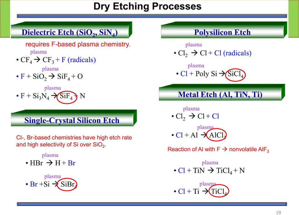
18 Features of Dry Etching 18

19 19
20 Comparison of Wet & Dry Etching (> 10nm) 20

21 LAB: Oxford Plasmalab 100 Loading Dock Gas flow Chamber 21
22 LAB: Oxford Plasmalab 100 Temperature: -150 o C to +400 o C Gases: Cl 2, SiCl 4, BCl 3, SF 6, Ar, O 2, H 2 and N 2 ICP and RF Power: Up to 300W 22
23 LAB: Al Etching Recipe Step 1. Step 2. Step 3. Step 4. Pressure (mtorr) RIE (W) ICP (W) Time (sec) Gas 1 (scmm) Ar: 50 BCL3: 30 BCL3: 30 Ar: 50 Gas 2 (scmm) CL2: 15 CL2: 8 Temperature(Celsius) Comment Purge the chamber Al2O3 etching Al etching Purge the chamber S1805 Al2O3 Al Native SiO2 Silicon Wafer ~500nm several nm ~200nm several nm ~200nm Al Step 2 Native SiO2 Step 3 Silicon Wafer Native SiO2 Silicon Wafer several nm ~200nm 23
24 S1805 Residual Removal Some S1805 left on the sample surface Removal Lift-off: Use Remover-PG to soak the substrate. Further Etching: O2 to remove organics. (potentially further oxidizes the Al) 24
25 Wire-grid Polarizer (100nm) Parallel Perpendicular Al SiO2 25
26 Review Etching and its terminologies Wet & Dry etching Plasma systems Ion milling Reactive ion etching Lab 26
27 Reference [1] etching.pdf [2] 450L11-Etching%20especially%20Plasma%20Etching.pdf [3] 27
28 Questions?? 28
III. Wet and Dry Etching
 III. Wet and Dry Etching Method Environment and Equipment Advantage Disadvantage Directionality Wet Chemical Solutions Atmosphere, Bath 1) Low cost, easy to implement 2) High etching rate 3) Good selectivity
Module 7 Wet and Dry Etching. Class Notes
 Module 7 Wet and Dry Etching Class Notes 1. Introduction Etching techniques are commonly used in the fabrication processes of semiconductor devices to remove selected layers for the purposes of pattern
Lecture 11. Etching Techniques Reading: Chapter 11. ECE 6450 - Dr. Alan Doolittle
 Lecture 11 Etching Techniques Reading: Chapter 11 Etching Techniques Characterized by: 1.) Etch rate (A/minute) 2.) Selectivity: S=etch rate material 1 / etch rate material 2 is said to have a selectivity
JePPIX Course Processing Wet and dry etching processes. Huub Ambrosius
 JePPIX Course Processing Wet and dry etching processes Huub Ambrosius Material removal: etching processes Etching is done either in dry or wet methods: Wet etching uses liquid etchants with wafers immersed
Dry Etch Process Application Note
 G-106-0405 pplication ulletin Dry Etch Process pplication Note nthony Ricci Etch Process Overview The etching process removes selected areas from wafer substrates. The two types of etching processes used
Coating Technology: Evaporation Vs Sputtering
 Satisloh Italy S.r.l. Coating Technology: Evaporation Vs Sputtering Gianni Monaco, PhD R&D project manager, Satisloh Italy 04.04.2016 V1 The aim of this document is to provide basic technical information
Etching Etch Definitions Isotropic Etching: same in all direction Anisotropic Etching: direction sensitive Selectivity: etch rate difference between
 Etching Etch Definitions Isotropic Etching: same in all direction Anisotropic Etching: direction sensitive Selectivity: etch rate difference between 2 materials Other layers below one being etch Masking
Damage-free, All-dry Via Etch Resist and Residue Removal Processes
 Damage-free, All-dry Via Etch Resist and Residue Removal Processes Nirmal Chaudhary Siemens Components East Fishkill, 1580 Route 52, Bldg. 630-1, Hopewell Junction, NY 12533 Tel: (914)892-9053, Fax: (914)892-9068
Electron Beam and Sputter Deposition Choosing Process Parameters
 Electron Beam and Sputter Deposition Choosing Process Parameters General Introduction The choice of process parameters for any process is determined not only by the physics and/or chemistry of the process,
Vacuum Evaporation Recap
 Sputtering Vacuum Evaporation Recap Use high temperatures at high vacuum to evaporate (eject) atoms or molecules off a material surface. Use ballistic flow to transport them to a substrate and deposit.
Plasma Etching ROCHESTER INSTITUTE OF TECHNOLOGY MICROELECTRONIC ENGINEERING. Plasma Etching. Dr. Lynn Fuller. http://people.rit.
 ROCHESTER INSTITUTE OF TECHNOLOGY MICROELECTRONIC ENGINEERING Plasma Etching Dr. Lynn Fuller http://people.rit.edu/lffeee 82 Lomb Memorial Drive Rochester, NY 14623-5604 Tel (585) 475-2035 Fax (585) 475-5041
Photolithography. Class: Figure 12.1. Various ways in which dust particles can interfere with photomask patterns.
 Photolithography Figure 12.1. Various ways in which dust particles can interfere with photomask patterns. 19/11/2003 Ettore Vittone- Fisica dei Semiconduttori - Lectio XIII 16 Figure 12.2. Particle-size
Introduction to VLSI Fabrication Technologies. Emanuele Baravelli
 Introduction to VLSI Fabrication Technologies Emanuele Baravelli 27/09/2005 Organization Materials Used in VLSI Fabrication VLSI Fabrication Technologies Overview of Fabrication Methods Device simulation
Grad Student Presentation Topics PHGN/CHEN/MLGN 435/535: Interdisciplinary Silicon Processing Laboratory
 Grad Student Presentation Topics 1. Baranowski, Lauryn L. AFM nano-oxidation lithography 2. Braid, Jennifer L. Extreme UV lithography 3. Garlick, Jonathan P. 4. Lochner, Robert E. 5. Martinez, Aaron D.
Conductivity of silicon can be changed several orders of magnitude by introducing impurity atoms in silicon crystal lattice.
 CMOS Processing Technology Silicon: a semiconductor with resistance between that of conductor and an insulator. Conductivity of silicon can be changed several orders of magnitude by introducing impurity
Study of Surface Reaction and Gas Phase Chemistries in High Density C 4 F 8 /O 2 /Ar and C 4 F 8 /O 2 /Ar/CH 2 F 2 Plasma for Contact Hole Etching
 TRANSACTIONS ON ELECTRICAL AND ELECTRONIC MATERIALS Vol. 16, No. 2, pp. 90-94, April 25, 2015 Regular Paper pissn: 1229-7607 eissn: 2092-7592 DOI: http://dx.doi.org/10.4313/teem.2015.16.2.90 OAK Central:
Plasma Cleaner: Physics of Plasma
 Plasma Cleaner: Physics of Plasma Nature of Plasma A plasma is a partially ionized gas consisting of electrons, ions and neutral atoms or molecules The plasma electrons are at a much higher temperatures
Study of tungsten oxidation in O 2 /H 2 /N 2 downstream plasma
 Study of tungsten oxidation in O 2 /H 2 /N 2 downstream plasma Songlin Xu a and Li Diao Mattson Technology, Inc., Fremont, California 94538 Received 17 September 2007; accepted 21 February 2008; published
Deposition Overview for Microsytems
 Deposition Overview for Microsytems Deposition PK Activity Terminology Participant Guide www.scme-nm.org Deposition Overview for Microsystems Primary Knowledge Participant Guide Description and Estimated
T.M.M. TEKNIKER MICROMACHINING
 T.M.M. TEKNIKER MICROMACHINING Micro and Nanotechnology Dapartment FUNDACION TEKNIKER Avda. Otaola. 20 Tel. +34 943 206744 Fax. +34 943 202757 20600 Eibar http://www.tekniker.es TMM FACILITIES -Clean Room
For Touch Panel and LCD Sputtering/PECVD/ Wet Processing
 production Systems For Touch Panel and LCD Sputtering/PECVD/ Wet Processing Pilot and Production Systems Process Solutions with over 20 Years of Know-how Process Technology at a Glance for Touch Panel,
Etching and Pattern Transfer (1) OUTLINE. 6.152J / 3.155J -- Spring Term 2005 Lecture 12 - Etch and Pattern Transfer I (Wet Etch) 1.
 OUTLINE. 6.152J / 3.155J -- Spring Term 2005 Lecture 12 - Etch and Pattern Transfer I (Wet Etch) 1.") 6.15JST05.Lecture1-1 1 Etching and Pattern Transer (1) OUTLINE Basic Concepts o Etching Wet Etching Speciic Wet Etches Silicon Silicon Dioxide Aluminum Dry (Plasma) Etch eview o Plasmas eading Assignment:
6.15JST05.Lecture1-1 1 Etching and Pattern Transer (1) OUTLINE Basic Concepts o Etching Wet Etching Speciic Wet Etches Silicon Silicon Dioxide Aluminum Dry (Plasma) Etch eview o Plasmas eading Assignment:
PLASMA TECHNOLOGY OVERVIEW
 PLASMA TECHNOLOGY OVERVIEW Plasmas are not a lab curiosity. Plasma processing has been an essential production tool for more than 30 years in the fabrication of microelectronic devices for example. Over
Ion Beam Sputtering: Practical Applications to Electron Microscopy
 Ion Beam Sputtering: Practical Applications to Electron Microscopy Applications Laboratory Report Introduction Electron microscope specimens, both scanning (SEM) and transmission (TEM), often require a
Lecture 12. Physical Vapor Deposition: Evaporation and Sputtering Reading: Chapter 12. ECE 6450 - Dr. Alan Doolittle
 Lecture 12 Physical Vapor Deposition: Evaporation and Sputtering Reading: Chapter 12 Evaporation and Sputtering (Metalization) Evaporation For all devices, there is a need to go from semiconductor to metal.
Process Diagnostics of Industrial Plasma Systems
 Process Diagnostics of Industrial Plasma Systems A thesis for the degree of PHILOSOPHIAE DOCTOR Presented to Dublin City University By Niall Mac Gearailt B.Eng. Faculty of Engineering and Computing Dublin
3.1 Etching wet etching, micromachining, dry etching, applications, diagnostics and end point detection, challenges in dry etching
 3.0 Etching and Chemo-Mechanical Polishing 3.1 Etching wet etching, micromachining, dry etching, applications, diagnostics and end point detection, challenges in dry etching 3.2 Chemo-Mechanical Polishing
High Rate Oxide Deposition onto Web by Reactive Sputtering from Rotatable Magnetrons
 High Rate Oxide Deposition onto Web by Reactive Sputtering from Rotatable Magnetrons D.Monaghan, V. Bellido-Gonzalez, M. Audronis. B. Daniel Gencoa, Physics Rd, Liverpool, L24 9HP, UK. www.gencoa.com,
Study of plasma-induced damage of porous ultralow-k dielectric films during photoresist stripping
 Study of plasma-induced damage of porous ultralow-k dielectric films during photoresist stripping Songlin Xu, a Ce Qin, Li Diao, Dave Gilbert, Li Hou, and Allan Wiesnoski Mattson Technology, Inc., Fremont,
Chapter 11 PVD and Metallization
 Chapter 11 PVD and Metallization 2006/5/23 1 Metallization Processes that deposit metal thin film on wafer surface. 2006/5/23 2 1 Metallization Definition Applications PVD vs. CVD Methods Vacuum Metals
Deposition of Thin Metal Films " (on Polymer Substrates)!
!") Deposition of Thin Metal Films " (on Polymer Substrates)! Shefford P. Baker! Cornell University! Department of Materials Science and Engineering! Ithaca, New York, 14853! MS&E 5420 Flexible Electronics,
Deposition of Thin Metal Films " (on Polymer Substrates)! Shefford P. Baker! Cornell University! Department of Materials Science and Engineering! Ithaca, New York, 14853! MS&E 5420 Flexible Electronics,
Neuere Entwicklungen zur Herstellung optischer Schichten durch reaktive. Wolfgang Hentsch, Dr. Reinhard Fendler. FHR Anlagenbau GmbH
 Neuere Entwicklungen zur Herstellung optischer Schichten durch reaktive Sputtertechnologien Wolfgang Hentsch, Dr. Reinhard Fendler FHR Anlagenbau GmbH Germany Contents: 1. FHR Anlagenbau GmbH in Brief
A Remote Plasma Sputter Process for High Rate Web Coating of Low Temperature Plastic Film with High Quality Thin Film Metals and Insulators
 A Remote Plasma Sputter Process for High Rate Web Coating of Low Temperature Plastic Film with High Quality Thin Film Metals and Insulators Dr Peter Hockley and Professor Mike Thwaites, Plasma Quest Limited
Supporting Online Material for
 www.sciencemag.org/cgi/content/full/1162193/dc1 Supporting Online Material for Polymer Pen Lithography Fengwei Huo, Zijian Zheng, Gengfeng Zheng, Louise R. Giam, Hua Zhang, Chad A. Mirkin* *To whom correspondence
How To Make A Plasma Control System
 XXII. Erfahrungsaustausch Mühlleiten 2015 Plasmaanalyse und Prozessoptimierung mittels spektroskopischem Plasmamonitoring in industriellen Anwendungen Swen Marke,, Lichtenau Thomas Schütte, Plasus GmbH,
Untitled Document. 1. Which of the following best describes an atom? 4. Which statement best describes the density of an atom s nucleus?
 Name: Date: 1. Which of the following best describes an atom? A. protons and electrons grouped together in a random pattern B. protons and electrons grouped together in an alternating pattern C. a core
Direct Energy Influx Measurements. in Low Pressure Plasma Processes
 Direct Energy Influx Measurements in Low Pressure Plasma Processes A.L. Thomann, GREMI Orléans R. Dussart, N. Semmar, J. Mathias, T. Lecas L. Bedra, P.A. Cormier, V. Dolique Outline I. Introduction: Why
The Periodic Table: Periodic trends
 Unit 1 The Periodic Table: Periodic trends There are over one hundred different chemical elements. Some of these elements are familiar to you such as hydrogen, oxygen, nitrogen and carbon. Each one has
Chemical Reactions During Wet-Etching Process of LSMO/PZT/LSMO-Structured Device Fabrication
 Ferroelectrics, 380:1, 97-101, 2009 Reprints available directly from the publisher DOI: 10.1080/00150190902873295 UR L: http://dx.doi.org/10.1080/00150190902873295 2009 Taylor & Francis ISSN: 0015-0193
A Plasma Doping Process for 3D FinFET Source/ Drain Extensions
 A Plasma Doping Process for 3D FinFET Source/ Drain Extensions JTG 2014 Cuiyang Wang*, Shan Tang, Harold Persing, Bingxi Wood, Helen Maynard, Siamak Salimian, and Adam Brand [email protected] Varian
Contamination. Cleanroom. Cleanroom for micro and nano fabrication. Particle Contamination and Yield in Semiconductors.
 Fe Particles Metallic contaminants Organic contaminants Surface roughness Au Particles SiO 2 or other thin films Contamination Na Cu Photoresist Interconnect Metal N, P Damages: Oxide breakdown, metal
Results Overview Wafer Edge Film Removal using Laser
 Results Overview Wafer Edge Film Removal using Laser LEC- 300: Laser Edge Cleaning Process Apex Beam Top Beam Exhaust Flow Top Beam Scanning Top & Top Bevel Apex Beam Scanning Top Bevel, Apex, & Bo+om
Solar Photovoltaic (PV) Cells
 Cells") Solar Photovoltaic (PV) Cells A supplement topic to: Mi ti l S Micro-optical Sensors - A MEMS for electric power generation Science of Silicon PV Cells Scientific base for solar PV electric power generation
Solar Photovoltaic (PV) Cells A supplement topic to: Mi ti l S Micro-optical Sensors - A MEMS for electric power generation Science of Silicon PV Cells Scientific base for solar PV electric power generation
3. What would you predict for the intensity and binding energy for the 3p orbital for that of sulfur?
 PSI AP Chemistry Periodic Trends MC Review Name Periodic Law and the Quantum Model Use the PES spectrum of Phosphorus below to answer questions 1-3. 1. Which peak corresponds to the 1s orbital? (A) 1.06
AN900 APPLICATION NOTE
 AN900 APPLICATION NOTE INTRODUCTION TO SEMICONDUCTOR TECHNOLOGY INTRODUCTION by Microcontroller Division Applications An integrated circuit is a small but sophisticated device implementing several electronic
Micro-Power Generation
 Micro-Power Generation Elizabeth K. Reilly February 21, 2007 TAC-meeting 1 Energy Scavenging for Wireless Sensors Enabling Wireless Sensor Networks: Ambient energy source Piezoelectric transducer technology
Semiconductor doping. Si solar Cell
 Semiconductor doping Si solar Cell Two Levels of Masks - photoresist, alignment Etch and oxidation to isolate thermal oxide, deposited oxide, wet etching, dry etching, isolation schemes Doping - diffusion/ion
Reactive Sputtering Using a Dual-Anode Magnetron System
 Reactive Sputtering Using a Dual-Anode Magnetron System A. Belkind and Z. Zhao, Stevens Institute of Technology, Hoboken, NJ; and D. Carter, G. McDonough, G. Roche, and R. Scholl, Advanced Energy Industries,
Graduate Student Presentations
 Graduate Student Presentations Dang, Huong Chip packaging March 27 Call, Nathan Thin film transistors/ liquid crystal displays April 4 Feldman, Ari Optical computing April 11 Guerassio, Ian Self-assembly
By Randy Heckman, Gregory Roche, James R. Usher of Advanced Energy Industries, Inc.
 WHITEPAPER By Randy Heckman, Gregory Roche, James R. Usher of Advanced Energy Industries, Inc. THE EVOLUTION OF RF POWER DELIVERY IN Radio frequency (RF) technology has been around since the beginnings
USING OPTICAL EMISSION SPECTROSCOPY TO IMPROVE EQUIPMENT UPTIME FOR AN AL2O3 ALD PROCESS *
 USING OPTICAL EMISSION SPECTROSCOPY TO IMPROVE EQUIPMENT UPTIME FOR AN AL2O3 ALD PROCESS * JOHN LOO Samsung Austin Semiconductor 12100 Samsung Blvd. Austin, Texas 78754 * Presented at the AVS 5 th International
CHEM 1411 Chapter 5 Homework Answers
 1 CHEM 1411 Chapter 5 Homework Answers 1. Which statement regarding the gold foil experiment is false? (a) It was performed by Rutherford and his research group early in the 20 th century. (b) Most of
Chapter 7 Periodic Properties of the Elements
 Chapter 7 Periodic Properties of the Elements 1. Elements in the modern version of the periodic table are arranged in order of increasing. (a). oxidation number (b). atomic mass (c). average atomic mass
ELEC 3908, Physical Electronics, Lecture 15. BJT Structure and Fabrication
 ELEC 3908, Physical Electronics, Lecture 15 Lecture Outline Now move on to bipolar junction transistor (BJT) Strategy for next few lectures similar to diode: structure and processing, basic operation,
Photolithography (source: Wikipedia)
") Photolithography (source: Wikipedia) For earlier uses of photolithography in printing, see Lithography. For the same process applied to metal, see Photochemical machining. Photolithography (also called
Photolithography (source: Wikipedia) For earlier uses of photolithography in printing, see Lithography. For the same process applied to metal, see Photochemical machining. Photolithography (also called
A Laboratory Approach to Semiconductor Process Technology
 A Laboratory Approach to Semiconductor Process Technology Mary Jane Willis Manufacturing Technology Program Albuquerque TVI, A Community College Albuquerque, New Mexico March, 1998 ABSTRACT The recent
J H Liao 1, Jianshe Tang 2,b, Ching Hwa Weng 2, Wei Lu 2, Han Wen Chen 2, John TC Lee 2
 Solid State Phenomena Vol. 134 (2008) pp 359-362 Online available since 2007/Nov/20 at www.scientific.net (2008) Trans Tech Publications, Switzerland doi:10.4028/www.scientific.net/ssp.134.359 Metal Hard
Demonstration of sub-4 nm nanoimprint lithography using a template fabricated by helium ion beam lithography
 Demonstration of sub-4 nm nanoimprint lithography using a template fabricated by helium ion beam lithography Wen-Di Li*, Wei Wu** and R. Stanley Williams Hewlett-Packard Labs *Current address: University
Types of Epitaxy. Homoepitaxy. Heteroepitaxy
 Epitaxy Epitaxial Growth Epitaxy means the growth of a single crystal film on top of a crystalline substrate. For most thin film applications (hard and soft coatings, optical coatings, protective coatings)
MICROPOSIT LOL 1000 AND 2000 LIFTOFF LAYERS For Microlithography Applications
 Technical Data Sheet MICROPOSIT LOL 1000 AND 2000 LIFTOFF LAYERS For Microlithography Applications Regional Product Availability Description Advantages North America Europe, Middle East and Africa Latin
Microstockage d énergie Les dernières avancées. S. Martin (CEA-LITEN / LCMS Grenoble)
") Microstockage d énergie Les dernières avancées S. Martin (CEA-LITEN / LCMS Grenoble) 1 Outline What is a microbattery? Microbatteries developped at CEA Description Performances Integration and Demonstrations
Microstockage d énergie Les dernières avancées S. Martin (CEA-LITEN / LCMS Grenoble) 1 Outline What is a microbattery? Microbatteries developped at CEA Description Performances Integration and Demonstrations
Chapter 5: Diffusion. 5.1 Steady-State Diffusion
 : Diffusion Diffusion: the movement of particles in a solid from an area of high concentration to an area of low concentration, resulting in the uniform distribution of the substance Diffusion is process
Lewis Dot Structures of Atoms and Ions
 Why? The chemical properties of an element are based on the number of electrons in the outer shell of its atoms. We use Lewis dot structures to map these valence electrons in order to identify stable electron
2015-2016 Facility Rates & Expense Caps
 NANOFAB FEES / SERVICES Entry Fee $20.00/Day $32.10/Day Nanofab Training Fee $25.00/Hour $40.13/Hour Nanofab Process Development/Labor $50.00/Hour $80.25/Hour Model Shop $25.00/Month $40.13/Month Wafer
WŝŽŶĞĞƌŝŶŐ > ĞdžƉĞƌŝĞŶĐĞ ƐŝŶĐĞ ϭϵϳϰ WŝĐŽƐƵŶ ^he > Ρ ZͲƐĞƌŝĞƐ > ƐLJƐƚĞŵƐ ƌŝěőŝŷő ƚśğ ŐĂƉ ďğƚǁğğŷ ƌğɛğăƌđś ĂŶĚ ƉƌŽĚƵĐƟŽŶ d, &hdhz K& d,/e &/>D /^, Z
 The ALD Powerhouse Picosun Defining the future of ALD Picosun s history and background date back to the very beginning of the field of atomic layer deposition. ALD was invented in Finland in 1974 by Dr.
Chemical dry etching of silicon nitride and silicon dioxide using CF 4 /O 2 /N 2 gas mixtures
 Chemical dry etching of silicon nitride and silicon dioxide using CF 4 /O 2 /N 2 gas mixtures B. E. E. Kastenmeier, a) P. J. Matsuo, J. J. Beulens, and G. S. Oehrlein b) Department of Physics, The University
Lezioni di Tecnologie e Materiali per l Elettronica
 Lezioni di Tecnologie e Materiali per l Elettronica Danilo Manstretta [email protected] microlab.unipv.it Outline Passive components Resistors Capacitors Inductors Printed circuits technologies
and LUMINOUS CHEMICAL VAPOR DEPOSITION INTERFACE ENGINEERING HirotsuguYasuda University of Missouri-Columbia Columbia, Missouri, U.S.A.
 LUMINOUS CHEMICAL VAPOR DEPOSITION and INTERFACE ENGINEERING HirotsuguYasuda University of Missouri-Columbia Columbia, Missouri, U.S.A. MARCEL MARCEL DEKKER. NEW YORK DEKKER Contents Preface iii Part I.
B) atomic number C) both the solid and the liquid phase D) Au C) Sn, Si, C A) metal C) O, S, Se C) In D) tin D) methane D) bismuth B) Group 2 metal
 atomic number C) both the solid and the liquid phase D) Au C) Sn, Si, C A) metal C) O, S, Se C) In D) tin D) methane D) bismuth B) Group 2 metal") 1. The elements on the Periodic Table are arranged in order of increasing A) atomic mass B) atomic number C) molar mass D) oxidation number 2. Which list of elements consists of a metal, a metalloid, and
1. The elements on the Periodic Table are arranged in order of increasing A) atomic mass B) atomic number C) molar mass D) oxidation number 2. Which list of elements consists of a metal, a metalloid, and
Sputtered AlN Thin Films on Si and Electrodes for MEMS Resonators: Relationship Between Surface Quality Microstructure and Film Properties
 Sputtered AlN Thin Films on and Electrodes for MEMS Resonators: Relationship Between Surface Quality Microstructure and Film Properties S. Mishin, D. R. Marx and B. Sylvia, Advanced Modular Sputtering,
Balzers Sputter Coater SCD 050
 Balzers Sputter Coater SCD 050 The SCD 050 is a bench top, sputter deposition system designed for thin films on substrates up to 6 inches. Morphology and thickness is user controlled using power, pressure,
Noble Gases. Outline Nobel Gas Elements Radon and Health Chemistry Homework
 Radon and Other Noble Gases The elements in the last column of the periodic table are all very stable, mono-atomic gases. Until 1962, they were called inert gases because they did not react with other
Chemical Sputtering. von Kohlenstoff durch Wasserstoff. W. Jacob
 Chemical Sputtering von Kohlenstoff durch Wasserstoff W. Jacob Centre for Interdisciplinary Plasma Science Max-Planck-Institut für Plasmaphysik, 85748 Garching Content: Definitions: Chemical erosion, physical
Arrangement of Electrons in Atoms
 CHAPTER 4 PRE-TEST Arrangement of Electrons in Atoms In the space provided, write the letter of the term that best completes each sentence or best answers each question. 1. Which of the following orbital
Honors Chemistry: Unit 6 Test Stoichiometry PRACTICE TEST ANSWER KEY Page 1. A chemical equation. (C-4.4)
") Honors Chemistry: Unit 6 Test Stoichiometry PRACTICE TEST ANSWER KEY Page 1 1. 2. 3. 4. 5. 6. Question What is a symbolic representation of a chemical reaction? What 3 things (values) is a mole of a chemical
Honors Chemistry: Unit 6 Test Stoichiometry PRACTICE TEST ANSWER KEY Page 1 1. 2. 3. 4. 5. 6. Question What is a symbolic representation of a chemical reaction? What 3 things (values) is a mole of a chemical
6.5 Periodic Variations in Element Properties
 324 Chapter 6 Electronic Structure and Periodic Properties of Elements 6.5 Periodic Variations in Element Properties By the end of this section, you will be able to: Describe and explain the observed trends
2. Deposition process
 Properties of optical thin films produced by reactive low voltage ion plating (RLVIP) Antje Hallbauer Thin Film Technology Institute of Ion Physics & Applied Physics University of Innsbruck Investigations
Name period AP chemistry Unit 2 worksheet Practice problems
 Name period AP chemistry Unit 2 worksheet Practice problems 1. What are the SI units for a. Wavelength of light b. frequency of light c. speed of light Meter hertz (s -1 ) m s -1 (m/s) 2. T/F (correct
Silicon-On-Glass MEMS. Design. Handbook
 Silicon-On-Glass MEMS Design Handbook A Process Module for a Multi-User Service Program A Michigan Nanofabrication Facility process at the University of Michigan March 2007 TABLE OF CONTENTS Chapter 1...
Chapter 10 CVD and Dielectric Thin Film
 Chapter 10 CVD and Dielectric Thin Film 2006/5/23 1 Objectives Identify at least four CVD applications Describe CVD process sequence List the two deposition regimes and describe their relation to temperature
IMA. Reaktives Ionenätzen für die Herstellung vertikaler, mikromechanisch aktuierbarer, optischer Bauelemente. Sören Irmer
 Sören Irmer Workshop "Oberflächentechnologie mit Plasma- und Ionenstrahlprozessen - Mühlleithen, 02. März 2004 Reaktives Ionenätzen für die Herstellung vertikaler, mikromechanisch aktuierbarer, optischer
Electroplating with Photoresist Masks
 Electroplating with Photoresist Masks Revised: 2014-01-17 Source: www.microchemicals.com/downloads/application_notes.html Electroplating - Basic Requirements on the Photoresist Electroplating with photoresist
Effects of Plasma Activation on Hydrophilic Bonding of Si and SiO 2
 PUBLICATION A Effects of Plasma Activation on Hydrophilic Bonding of Si and SiO 2 Journal of The Electrochemical Society, Vol. 149, No. 6, (2002), pp. G348 G351. Reprinted by permission of ECS The Electrochemical
SCPS Chemistry Worksheet Periodicity A. Periodic table 1. Which are metals? Circle your answers: C, Na, F, Cs, Ba, Ni
 SCPS Chemistry Worksheet Periodicity A. Periodic table 1. Which are metals? Circle your answers: C, Na, F, Cs, Ba, Ni Which metal in the list above has the most metallic character? Explain. Cesium as the
Application of SEERS to real time Plasma Monitoring in Production at different FABs
 AECAPC SYMPOSIUM 2001, BANFF Application of SEERS to real time Plasma Monitoring in Production at different FABs Volker Tegeder Sensor Evaluation Calculation of expected Economical Benefit Automatic link
Chapter 5 TEST: The Periodic Table name
 Chapter 5 TEST: The Periodic Table name HPS # date: Multiple Choice Identify the choice that best completes the statement or answers the question. 1. The order of elements in the periodic table is based
2. Nanoparticles. Introduction to Nanoscience, 2005 1
 2. Nanoparticles Nanoparticles are the simplest form of structures with sizes in the nm range. In principle any collection of atoms bonded together with a structural radius of < 100 nm can be considered
AP CHEMISTRY 2009 SCORING GUIDELINES
 AP CHEMISTRY 2009 SCORING GUIDELINES Question 6 (8 points) Answer the following questions related to sulfur and one of its compounds. (a) Consider the two chemical species S and S 2. (i) Write the electron
Periodic Table Questions
 Periodic Table Questions 1. The elements characterized as nonmetals are located in the periodic table at the (1) far left; (2) bottom; (3) center; (4) top right. 2. An element that is a liquid at STP is
The Advanced Placement Examination in Chemistry. Part I Multiple Choice Questions Part II Free Response Questions Selected Questions from1970 to 2010
 The Advanced Placement Examination in Chemistry Part I Multiple Choice Questions Part II Free Response Questions Selected Questions from1970 to 2010 Atomic Theory and Periodicity Part I 1984 1. Which of
5.4 Trends in the Periodic Table
 5.4 Trends in the Periodic Table Think about all the things that change over time or in a predictable way. For example, the size of the computer has continually decreased over time. You may become more
EE-527: MicroFabrication
 EE-527: MicroFabrication Wet Etching Outline Isotropic Si etching Anisotropic Si etching Anisotropic GaAs etching Isotropic etching of SiO 2, Al, and Cr General features of wet chemical etching Selective
Chapter Outline. 3 Elements and Compounds. Elements and Atoms. Elements. Elements. Elements 9/4/2013
 3 Elements and Compounds Chapter Outline 3.1 Elements A. Distribution of Elements Foundations of College Chemistry, 14 th Ed. Morris Hein and Susan Arena Copyright This reclining Buddha in Thailand is
Advanced VLSI Design CMOS Processing Technology
 Isolation of transistors, i.e., their source and drains, from other transistors is needed to reduce electrical interactions between them. For technologies
Surface activation of plastics by plasma for adhesion promotion
 Surface activation of plastics by plasma for adhesion promotion Uwe Stöhr, Ph. D. 1 Introduction In many fields a good adhesion between two materials is necessary. The adhesion should exist at the whole
Photons. ConcepTest 27.1. 1) red light 2) yellow light 3) green light 4) blue light 5) all have the same energy. Which has more energy, a photon of:
 red light 2) yellow light 3) green light 4) blue light 5) all have the same energy. Which has more energy, a photon of:") ConcepTest 27.1 Photons Which has more energy, a photon of: 1) red light 2) yellow light 3) green light 4) blue light 5) all have the same energy 400 nm 500 nm 600 nm 700 nm ConcepTest 27.1 Photons Which
ConcepTest 27.1 Photons Which has more energy, a photon of: 1) red light 2) yellow light 3) green light 4) blue light 5) all have the same energy 400 nm 500 nm 600 nm 700 nm ConcepTest 27.1 Photons Which
The Lewis structure is a model that gives a description of where the atoms, charges, bonds, and lone pairs of electrons, may be found.
 CEM110 Week 12 Notes (Chemical Bonding) Page 1 of 8 To help understand molecules (or radicals or ions), VSEPR shapes, and properties (such as polarity and bond length), we will draw the Lewis (or electron