Dr Marcin Adamiak marcin.adamiak.
|
|
|
- Eunice Cummings
- 8 years ago
- Views:
Transcription
1 FP7 NMP/INCO Brokerage Event Warsaw, September 2009 Dr Marcin Adamiak marcin.adamiak Institute of Engineering Materials and Biomaterials Silesian University of Technology,, GliwiceG liwice, Poland

2 SILESIAN UNIVERSITY Surface modification OF TECHNOLOGY of engineering GLIWICE, materials by POLAND PVD coatings 2 2

3 Dr SILESIAN Marcin Adamiak UNIVERSITY OF TECHNOLOGY GLIWICE, POLAND

4 Laser surface treatment of multicrystalline silicon for enhancing optical properties Leszek A. Dobrzański, Gliwice, Poland Laser surface treatment of multicrystalline silicon for photovoltaic application Prof. L.A. Dobrzański A. Drygała, a, K. Gołombek ombek,, P. Panek, E. Bielańska, P. Zięba Institute of Engineering Materials and Biomaterials Silesian University of Technology,, GliwiceG liwice, Poland

5 Laser surface treatment of multicrystalline silicon for enhancing optical properties Leszek A. Dobrzański, Gliwice, Poland Interaction between the incident sunlight and planar surface

6 Laser surface treatment of multicrystalline silicon for enhancing optical properties Leszek A. Dobrzański, Gliwice, Poland The influence of surface texture on light reflection

7 Laser surface treatment of multicrystalline silicon for enhancing optical properties Leszek A. Dobrzański, Gliwice, Poland Laser surface treatment of multicrystalline silicon laser beam wafer after laser treatment wafer before laser treatment

8 Laser surface treatment of multicrystalline silicon for enhancing optical properties Leszek A. Dobrzański, Gliwice, Poland Results a) b) c) 100µm 100µm 100µm SEM images of multicrystalline silicon surface a) after saw damage etching but before laser texturisation, b) with laser texture in the form of parallel grooves c) with laser texture in the form of perpendicular grooves
 with laser texture in the form of perpendicular")
9 Laser surface treatment of multicrystalline silicon for enhancing optical properties Leszek A. Dobrzański, Gliwice, Poland b) a) 100µm 100µm SEM images of multicrystalline silicon surface after laser texturisation and 20 min etching with texture in the form of a) parallel grooves b),c) perpendicular grooves c) 100µm

10 Laser surface treatment of multicrystalline silicon for enhancing optical properties Leszek A. Dobrzański, Gliwice, Poland before laser texturization after laser texturization after laser texturization and 10 min etching after laser texturization and 20 min etching Results 40 R [%] λ [nm] Reflection curves for wafers with texture in the form of perpendicular grooves
![texturization and 10 min etching after laser texturization and 20 min etching Results 40 R [%] 30 20 10 0](/docs-images/41/2835222/images/page_10.jpg "300 400 500 600 700 800 900 1000 1100 1200 1300 λ [nm] Reflection curves for wafers with texture in the form")
11 Laser surface treatment of multicrystalline silicon for enhancing optical properties Leszek A. Dobrzański, Gliwice, Poland FP7 NMP/INCO Brokerage Event Warsaw, September 2009 Surface modification of engineering materials by PVD nano-coatings deposition Institute of Engineering Materials and Biomaterials Silesian University of Technology,, GliwiceG liwice, Poland

12
13 Hard and Wear-Resistant coatings applications

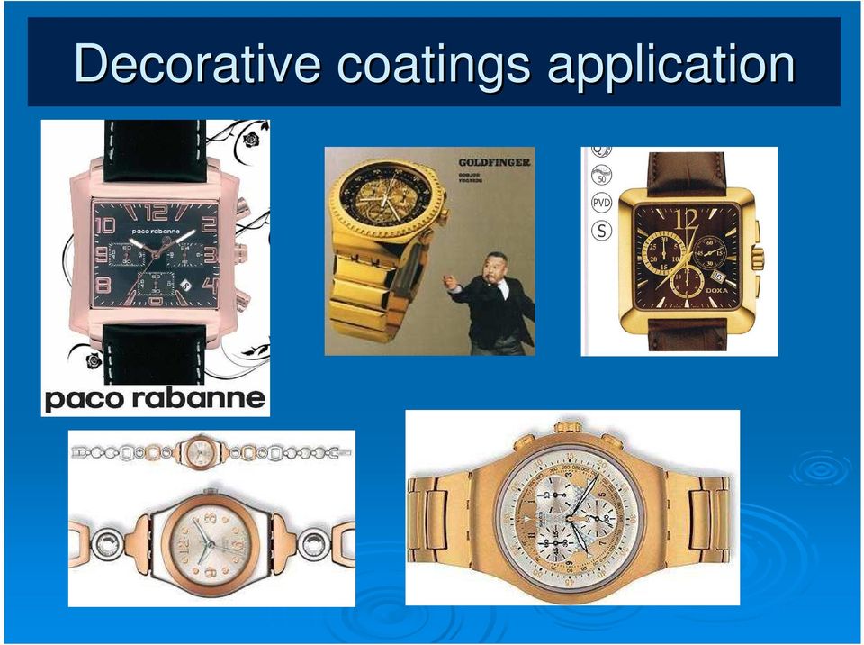
14 Decorative coatings application
15 Coating Advantages and Usage Cutting The hard coatings reduce the abrasive, adhesive and crater wear on the tools for conventional wet, dry and high speed machining. Modern coating technology reduces ARC droplets and the friction between chip and tool.

16 Coating Advantages and Usage Tribology Hard coatings solve tribological problems with machine components that can be coated at temperatures of C. Due to the hardness (up to 36 GPa), abrasive wear is reduced. This leads to higher reliability for dry operations and environmen -tally damaging lubricants can be replaced.

17 Coatings and Substrates Coating composition Process type TiN PVD Ti(C,N) PVD Ti(Al,N) PVD TiN+(Ti,Al,Si)N+TiN PVD TiN+multi(Ti,Al,Si)N+TiN PVD TiN+(Ti,Al,Si)N+(Al,Si,Ti)N PVD TiN+TiC+TiN PVD Ti(C,N)+TiN CVD Ti(C,N)+Al 2 O 3 +TiN CVD Ti(C,N)+Al 2 O 3 +TiC CVD TiN+Al 2 O 3 CVD TiN+Al 2 O 3 +TiN CVD TiN+Al 2 O 3 +TiN+Al 2 O 3 +TiN CVD TiC+Ti(C,N)+Al 2 O 3 +TiN CVD Substrates High Speed Steels Cemented Carbides Cermets Si 3 N 4 Ceramics Al 2 O 3 +ZrO 2 Ceramics Al 2 O 3 +TiC Ceramics Al 2 O 3 +SiC (w) Ceramics

18 a) b) Surface topography of the TiN coating deposited on HSS (coating deposition conditions: a) substrate bias 0V, b) substrate bias 200V).
 substrate")
19 Structures of the coatings a) b) Fracture of the: a) Ti/TiAlN x 1, b) Ti/CrN x 150 coatings 19
 Ti/CrN x 150")
20 a) b) Fracture of the TiN coating deposited on HSS (coating deposition conditions: a) substrate bias 0V, b) substrate bias 200V).
 substrate bias 0V, b)")
21 Structures of the coatings a) b) Fracture of the: a) Ti/CrN x 15, b) TiAlN/Mo x 15 coatings 21
22 Chemical composition Changes of concentrations of constituents of the Ti/TiAlN x 15 coating and of the substrate materials 22
23 Cutting ability Wear VB [mm] 0,35 0,3 0,25 0,2 0,15 0,1 0,05 y = 0,0007x - 0,009x + 0,0649x R = 0,9982 y = 3E-05x - 0,0005x + 0,0184x R = 0, uncoated TiN+Al 2O3 Time t [min]
24 Finite Element Methods model - results Distribution of the simulated compression stresses in the TiN coating Coating thickness t=10 µm, process temperature 540 C, specimen distance from the magnetron disk 125 mm σ max =944 MPa Coating thickness t=2,2 µm, process temperature 500 C, specimen distance from the magnetron disk 125 mm σ max =1334 MPa
25 FP7 NMP/INCO Brokerage Event Warsaw, September 2009 Surface modification by laser surface treatment LST Amorphous and nanocrystaline magnetic composite materials Metal Matrix Composite, Polymer Matrix composites Computational Material Science (Artificial neural networks, FEM, Fractal Analysis) Powder metallurgy and Metal Injection Moulding Microstructural characterisation by LM, SEM, TEM, XRD, EBDS, WDS, EDS Other characteristics
26 Prof.L.A.Dobrzański M.Dr HC DIRECTOR INSTITUTE OF ENGINEERING MATERIALS AND BIOMATERIALS SILESIAN UNIVERSITY OF TECHNOLOGY GLIWICE,POLAND PRESIDENT WORLD ACADEMY OF MATERIALS AND MANUFACTURING ENGINEERING Institute of Engineering Materials and Biomaterials Silesian University of Technology,, GliwiceG liwice, Poland
27 Thank you very much for your kind attention Dr M. Adamiak
Pamukkale Üniversitesi Mühendislik Bilimleri Dergisi. Pamukkale University Journal of Engineering Sciences
 Pamukkale Üniversitesi Mühendislik Bilimleri Dergisi, Cilt 19, Sayı 7 (IMSP 2013 Özel Sayı), Sayfalar 275-280 Pamukkale Üniversitesi Mühendislik Bilimleri Dergisi Pamukkale University Journal of Engineering
COATED CARBIDE. TiN. Al 2 O 3
 COATED CARBIDE GENERAL INFORMATION CVD = Chemical Vapour Deposition coated grades GC2015, GC2025, GC2135, GC235, GC3005, GC3015, GC3020, GC3025, GC3115, GC4015, GC4025, GC4035, S05F, and CD1810. PVD =
Grade Selection... Coated Grades / CVD... Coated Grades / PVD... Cermet... PCBN (T-CBN)... PCD (T-DIA)... Ceramics...
... PCD (T-DIA)... Ceramics...") Products Grade Selection... Coated / CVD... Coated / PVD... Cermet... PCBN (T-CBN)... PCD (T-DIA)... Ceramics... Uncoated Cemented Carbides... Ultra fine Grain Cemented Carbides... -2-4 -6-8 -0-2 - -4-5
Products Grade Selection... Coated / CVD... Coated / PVD... Cermet... PCBN (T-CBN)... PCD (T-DIA)... Ceramics... Uncoated Cemented Carbides... Ultra fine Grain Cemented Carbides... -2-4 -6-8 -0-2 - -4-5
CUTTING TOOL TECHNOLOGY. 1. Tool life 2. Tool Materials 3. Tool Geometry 4. Cutting fluids
 CUTTING TOOL TECHNOLOGY 1. Tool life 2. Tool Materials 3. Tool Geometry 4. Cutting fluids 1 Introduction Machining is accomplished by cutting tools. Cutting tools undergo high force and temperature and
Functional Gradient Hardmetals: From Research To Application
 New Materials - B2B/B2R&B, 21.Nov.2011, Bratislava/SK Functional Gradient Hardmetals: From Research To Application Walter Lengauer Vienna University of Technology PHYSICAL METALLURGY GROUP Prof. W. Lengauer
Summary of Insert Grades. Insert Lineup Turning Milling Drilling Insert Selection Table Grade Properties PCD CBN. Ceramic. Cell Fiber. Cermet.
 1~15 Summary of Insert Lineup Milling Drilling Insert Selection Table Grade Properties PCD Ceramic Cell Fiber PVD Coated CVD Coated PVD Coated for PVD Coated for Milling and Drilling 2~7 2~3 4 5 5 6 7
Cutting force, Fc (N) ' 270. 100 110 120 130 Cutting speed (m/min)
 ' 270. 100 110 120 130 Cutting speed (m/min)") 159 Rake face Adhesion Rake face Nose wear Tool life = 50.2 min Nose wear Tool life = 30.9 min Figure 4.19 - Nose wear at the cutting edge of T4 coated carbide insert after machining Ti- 6Al-4V alloy with
159 Rake face Adhesion Rake face Nose wear Tool life = 50.2 min Nose wear Tool life = 30.9 min Figure 4.19 - Nose wear at the cutting edge of T4 coated carbide insert after machining Ti- 6Al-4V alloy with
HARD MILLING OPERATION OF AISI O2 COLD WORK TOOL STEEL BY CARBIDE TOOLS PROTECTED WITH DIFFERENT HARD COATINGS
 JESTECH, 15(1), 21-26, (2012) JESTECH HARD MILLING OPERATION OF AISI O2 COLD WORK TOOL STEEL BY CARBIDE TOOLS PROTECTED WITH DIFFERENT HARD COATINGS Halil Çalışkan *, Cahit Kurbanoğlu **, Davorin Kramar
Module 3 Machinability. Version 2 ME, IIT Kharagpur
 Module 3 Machinability Lesson 1 Cutting Tool Materials of common use Instructional Objectives At the end of this lesson, the students will be able to (i) Identify the needs and cite the chronological development
How To Make A Diamond Diamond Wirehead From A Diamond
 ACKNOWLEDGMENTS This work would not have been possible without the advice and support of many people. First, and foremost, I would like to thank my advisor Dr. John Patten for providing me the opportunity
2. Deposition process
 Properties of optical thin films produced by reactive low voltage ion plating (RLVIP) Antje Hallbauer Thin Film Technology Institute of Ion Physics & Applied Physics University of Innsbruck Investigations
Laser beam sintering of coatings and structures
 Laser beam sintering of coatings and structures Anne- Maria Reinecke, Peter Regenfuß, Maren Nieher, Sascha Klötzer, Robby Ebert, Horst Exner Laserinstitut Mittelsachsen e.v. an der Hochschule Mittweida,
Think precision, Think HSS REAMING
 Think precision, Think HSS REAMING SUMMARY REAMING TOOLS 2 Zoom on a reamer 3 Which HSS for maximum efficiency? 4 Coatings for the best performance 5 Vocabulary 6 Choose the right design 7 Types of bevel
UDDEHOLM VANADIS 30 SUPERCLEAN
 UDDEHOLM VANADIS 30 SUPERCLEAN UDDEHOLMS AB No part of this publication may be reproduced or transmitted for commercial purposes without permission of the copyright holder. This information is based on
U-Max Chamfering endmill SPMT-WL 0.17 (0.08-0.21) -WH 0.35 (0.10-0.42) R215.64. Long edge cutter 215.3 0.17 (0.10-0.20) R215.3 -AAH 0.12 (0.08-0.
 -WH 0.35 (0.10-0.42) R215.64. Long edge cutter 215.3 0.17 (0.10-0.20) R215.3 -AAH 0.12 (0.08-0.") General Turning PROFILING Feed recommendations Feed per tooth, fz (mm/tooth) Insert geometry Insert size Starting value (min.- max.) U-Max Chamfering endmill SPMT-WL 0.17 (0.08-0.21) -WH 0.35 (0.10-0.42)
General Turning PROFILING Feed recommendations Feed per tooth, fz (mm/tooth) Insert geometry Insert size Starting value (min.- max.) U-Max Chamfering endmill SPMT-WL 0.17 (0.08-0.21) -WH 0.35 (0.10-0.42)
Cutting Tool Materials
 Training Objectives After watching the video and reviewing this printed material, the viewer will gain knowledge and understanding of cutting tool metallurgy and specific tool applications for various
VeMet, Utrecht, NL «Solution in Wear Protection» 26.10.2011 Dipl.-Ing. Wolfgang Leichnitz. Quit
 VeMet, Utrecht, NL «Solution in Wear Protection» 26.10.2011 Dipl.-Ing. Wolfgang Leichnitz Quit Theory and Practice of Wear Definition In materials science, wear is the erosion of material from a solid
Zelf-herstellende keramische oppervlakken Bijeenkomst: Falen of presteren van deklagen het slijtageproces 27 april 2011
 Zelf-herstellende keramische oppervlakken Bijeenkomst: Falen of presteren van deklagen het slijtageproces 27 april 2011 Matthijn de Rooij University of Twente Laboratory for Surface Technology and Tribology
THIN FILM MATERIALS TECHNOLOGY
 THIN FILM MATERIALS TECHNOLOGY Sputtering of Compound Materials by Kiyotaka Wasa Yokohama City University Yokohama, Japan Makoto Kitabatake Matsushita Electric Industrial Co., Ltd. Kyoto, Japan Hideaki
APPLICATION OF X-RAY COMPUTED TOMOGRAPHY IN SILICON SOLAR CELLS
 APPLICATION OF X-RAY COMPUTED TOMOGRAPHY IN SILICON SOLAR CELLS V.A. Popovich 1, W. Verwaal 2, M. Janssen 1, I. J. Bennett 3, I.M.Richardson 1, 1. Delft University of Technology, Department of Materials
w w w. a u t o s t e e l. o r g
 Great Designs in Steel is Sponsored by: AK Steel Corporation, ArcelorMittal Dofasco, ArcelorMittal USA, Nucor Corporation, Severstal North America and United States Steel Corporation LIGHTWEIGHTING AUTOMOTIVE
How To Make A Pvd Coating
 Hard and Superhard Nanocomposite Coating deposited by PVD technology for industrial application Dott. Romagnoli Denis STS Service and Tools STS s.r.l. via Parini 12 40033 Casalecchio di Reno(Bo) Tel. 051-969882
Three Key Elements of a Cutting Tool
 End Mill Training Three Key Elements of a Cutting Tool Geometry Cutting Tool 3 Elements Needed in a Good Cutting Tool Well Balanced For Best Performance Only Good as the Weakest Link End Mill Terms A -
CIRP Encyclopedia of Production Engineering
 The International Academy for Production Engineering Luc Laperriere Gunther Reinhart Editors CIRP Encyclopedia of Production Engineering Volume 1 A-H With 1145 Figures and 85 Tables ^ Springer Reference
Manufacturing Tooling Cutting Tool Design. Elements of Machining. Chip Formation. Nageswara Rao Posinasetti
 Manufacturing Tooling Cutting Tool Design Nageswara Rao Posinasetti Elements of Machining Cutting tool Tool holding Guiding device Work piece Machine tool January 29, 2008 Nageswara Rao Posinasetti 2 Chip
Phenomenological aspects of a modified fragmentation of the ground material
 Phenomenological aspects of a modified fragmentation of the ground material Lucjan Dabrowski, Mieczyslaw Marciniak Warsaw University of Technology, Warsaw, Poland Summary: The main point of this paper
ORIENTATION CHARACTERISTICS OF THE MICROSTRUCTURE OF MATERIALS
 ORIENTATION CHARACTERISTICS OF THE MICROSTRUCTURE OF MATERIALS K. Sztwiertnia Polish Academy of Sciences, Institute of Metallurgy and Materials Science, 25 Reymonta St., 30-059 Krakow, Poland MMN 2009
Tableting Punch Performance Can Be Improved With Precision Coatings
 Tableting Punch Performance Can Be Improved With Precision Coatings by Arnold H. Deutchman, Ph. D. Director of Research and Development (614) 873-4529 X 114 adeutchman@beamalloy.net Mr. Dale C. Natoli
Laser sintering of greens compacts of MoSi 2
 Laser sintering of greens compacts of MoSi 2 G. de Vasconcelos 1, R. Cesar Maia 2, C.A.A.Cairo 3, R. Riva 2, N.A.S.Rodrigues 2, F.C.L.Mello 3 Instituto de Estudos Avançados 1, Instituto Tecnológico de
OPTIMIZING OF THERMAL EVAPORATION PROCESS COMPARED TO MAGNETRON SPUTTERING FOR FABRICATION OF TITANIA QUANTUM DOTS
 OPTIMIZING OF THERMAL EVAPORATION PROCESS COMPARED TO MAGNETRON SPUTTERING FOR FABRICATION OF TITANIA QUANTUM DOTS Vojtěch SVATOŠ 1, Jana DRBOHLAVOVÁ 1, Marian MÁRIK 1, Jan PEKÁREK 1, Jana CHOMOCKÁ 1,
BIOACTIVE COATINGS ON 316L STAINLESS STEEL IMPLANTS
 Trends Biomater. Artif. Organs. Vol. 17(2) pp 43-47 (2004) http//www.sbaoi.org BIOACTIVE COATINGS ON 316L STAINLESS STEEL IMPLANTS N. Ramesh Babu*,+, Sushant Manwatkar*, K. Prasada Rao* and T. S. Sampath
HPPMS/DC-MSIP (Cr,Al,V)N and (Cr,Al,W)N Thin Films for High Temperature Application
N and (Cr,Al,W)N Thin Films for High Temperature Application") HPPMS/DC-MSIP (Cr,Al,V)N and (Cr,Al,W)N Thin Films for High Temperature Application Sebastian Theiß K. Bobzin, N. Bagcivan, M. Ewering, R. H. Brugnara April 23, 21 HPPMS/HiPIMS/MPP Workshop, Golden Outline
HPPMS/DC-MSIP (Cr,Al,V)N and (Cr,Al,W)N Thin Films for High Temperature Application Sebastian Theiß K. Bobzin, N. Bagcivan, M. Ewering, R. H. Brugnara April 23, 21 HPPMS/HiPIMS/MPP Workshop, Golden Outline
Lapping and Polishing Basics
 Lapping and Polishing Basics Applications Laboratory Report 54 Lapping and Polishing 1.0: Introduction Lapping and polishing is a process by which material is precisely removed from a workpiece (or specimen)
CHAPTER 6 WEAR TESTING MEASUREMENT
 84 CHAPTER 6 WEAR TESTING MEASUREMENT Wear is a process of removal of material from one or both of two solid surfaces in solid state contact. As the wear is a surface removal phenomenon and occurs mostly
Multi-walled Carbon Nanotube Reinforced Aluminum Nanocomposites by Cold Kinetic Spraying
 Multi-walled Carbon Nanotube Reinforced Aluminum Nanocomposites by Cold Kinetic Spraying SRINIVASA R BAKSHI 1, and ARVIND AGARWAL 2 1,2 Florida International University, Miami, FL 33174, USA. E-mail: agarwala@fiu.edu
R&D Services Knowledge transfer
 R&D Services Knowledge transfer Training Offer - November 2009 OCAS : a joint venture between ArcelorMittal and the Flemish Region R&D Knowledge transfer - Scope Market-oriented knowledge transfer in the
Uddeholm Vanadis 4 Extra SuperClean. Uddeholm Vanadis 4 Extra SuperClean
 Uddeholm Vanadis 4 Extra SuperClean 1 Uddeholm Vanadis 4 Extra SuperClean CONSISTENT TOOL PERFORMANCE LONG AND RELIABLE TOOL LIFE With an increased demand for just in time deliveries (JIT) and shorter
Fraunhofer Institute for Material and Beam Technology
 Laser Micro Processing Dr. Udo Klotzbach Fraunhofer Institute for Material and Beam Technology Dresden Overview Equipment - CO 2 -lasers - Solid state lasers (Nd:YAG, Disk, Fiber) - Diode lasers - Excimer
Conductivity of silicon can be changed several orders of magnitude by introducing impurity atoms in silicon crystal lattice.
 CMOS Processing Technology Silicon: a semiconductor with resistance between that of conductor and an insulator. Conductivity of silicon can be changed several orders of magnitude by introducing impurity
Results Overview Wafer Edge Film Removal using Laser
 Results Overview Wafer Edge Film Removal using Laser LEC- 300: Laser Edge Cleaning Process Apex Beam Top Beam Exhaust Flow Top Beam Scanning Top & Top Bevel Apex Beam Scanning Top Bevel, Apex, & Bo+om
Hanshan Dong Birmingham Surface Engineering Group The University of Birmingham
 Advanced Surface Engineering Technologies for Remanufacturing Hanshan Dong Birmingham Surface Engineering Group The University of Birmingham UK - China Joint Project Towards long-life remanufactured heavy-duty
Evaluating Surface Roughness of Si Following Selected Lapping and Polishing Processes
 Applications Laboratory Report 86 Evaluating Surface Roughness of Si Following Selected Processes Purpose polishing of samples is a common application and required for a variety of manufacturing and research
Rapid Prototyping and Development of Microfluidic and BioMEMS Devices
 Rapid Prototyping and Development of Microfluidic and BioMEMS Devices J. Sasserath and D. Fries Intelligent Micro Patterning System Solutions, LLC St. Petersburg, Florida (T) 727-522-0334 (F) 727-522-3896
COMPOSITE MATERIALS. Asst. Prof. Dr. Ayşe KALEMTAŞ
 COMPOSITE MATERIALS Office Hours: Tuesday, 16:30-17:30 akalemtas@mu.edu.tr, akalemtas@gmail.com Phone: +90 252 211 19 17 Metallurgical and Materials Engineering Department ISSUES TO ADDRESS Classification
Manufacturing Technology II. Exercise 6. Tool materials for forming tools
 Lehrstuhl für Technologie der Fertigungsverfahren Laboratorium für Werkzeugmaschinen und Betriebslehre Manufacturing Technology II Exercise 6 Tool materials for forming tools Werkzeugmaschinenlabor Lehrstuhl
Tribology in Industry. Vanadium Alloyed PVD CrAlN Coatings for Friction Reduction in Metal Forming Applications
 Vol. 34, N o 2 (2012) 101-107 Tribology in Industry www.tribology.fink.rs RESEARCH Vanadium Alloyed PVD CrAlN Coatings for Friction Reduction in Metal Forming Applications K. Bobzin a, N. Bagcivan a, M.
Plasma Electronic is Partner of. Tailor-Made Surfaces by Plasma Technology
 Precision Fair 2013 Stand 171 Plasma Electronic is Partner of Tailor-Made Surfaces by Plasma Technology Dr. J. Geng, Plasma Electronic GmbH Modern Surface Technology in 1900 Overview A short introduction
Final Report. Period Start Date: October 1, 2000 Period End Date: September 30, 2002
 Development of Advanced Drill Components for BHA Using Microwave Technology Incorporating Carbide, Diamond Composites and Functionally Graded Materials Final Report Period Start Date: October 1, 2000 Period
Photolithography. Class: Figure 12.1. Various ways in which dust particles can interfere with photomask patterns.
 Photolithography Figure 12.1. Various ways in which dust particles can interfere with photomask patterns. 19/11/2003 Ettore Vittone- Fisica dei Semiconduttori - Lectio XIII 16 Figure 12.2. Particle-size
The New PVD HI3-Technology: Latest Developments and Potential for Coining Dies.
 The New PVD HI3-Technology: Latest Developments and Potential for Coining Dies. Technical Forum - World Money Fair 2015, Berlin 29 th January 2015, Oerlikon The New Segment Surface Solutions Segment Manmade
Sputtered AlN Thin Films on Si and Electrodes for MEMS Resonators: Relationship Between Surface Quality Microstructure and Film Properties
 Sputtered AlN Thin Films on and Electrodes for MEMS Resonators: Relationship Between Surface Quality Microstructure and Film Properties S. Mishin, D. R. Marx and B. Sylvia, Advanced Modular Sputtering,
Chapter 2 Fractal Analysis in CNC End Milling
 Chapter 2 Fractal Analysis in CNC End Milling Abstract This chapter deals with the fractal dimension modeling in CNC end milling operation. Milling operations are carried out for three different materials
Neuere Entwicklungen zur Herstellung optischer Schichten durch reaktive. Wolfgang Hentsch, Dr. Reinhard Fendler. FHR Anlagenbau GmbH
 Neuere Entwicklungen zur Herstellung optischer Schichten durch reaktive Sputtertechnologien Wolfgang Hentsch, Dr. Reinhard Fendler FHR Anlagenbau GmbH Germany Contents: 1. FHR Anlagenbau GmbH in Brief
1. Introduction I. SULIMA. TRIBOLOGICAL PROPERTIES OF STEEL/TiB 2 COMPOSITES PREPARED BY SPARK PLASMA SINTERING
 A R C H I V E S O F M E T A L L U R G Y A N D M A T E R I A L S Volume 59 2014 Issue 4 DOI: 10.2478/amm-2014-0216 I. SULIMA TRIBOLOGICAL PROPERTIES OF STEEL/TiB 2 COMPOSITES PREPARED BY SPARK PLASMA SINTERING
SS-EN ISO 9001 SS-EN ISO 14001
 This information is based on our present state of knowledge and is intended to provide general notes on our products and their uses. It should not therefore be construed as a warranty of specific properties
Materials Sciences. Dr.-Ing. Norbert Hort norbert.hort@gkss.de. International Masters Programme in Biomedical Engineering
 Materials Sciences International Masters Programme in Biomedical Engineering Magnesium Innovations Center (MagIC) GKSS Forschungszentrum Geesthacht GmbH Dr.-Ing. Norbert Hort norbert.hort@gkss.de Contents
Graduate Student Presentations
 Graduate Student Presentations Dang, Huong Chip packaging March 27 Call, Nathan Thin film transistors/ liquid crystal displays April 4 Feldman, Ari Optical computing April 11 Guerassio, Ian Self-assembly
EUROLAB 25 years. The role of metrology and testing to characterize materials and products. EUROLAB 25th Anniversary Seminar
 EUROLAB 25 years The role of metrology and testing to characterize materials and products April 9, 2015, Odense Danmark 1 Origin of Conformity Assessment The New Approach for the European Economic Community
Plating on Aluminium
 TALAT Lecture 5205 Plating on Aluminium 19 pages, 23 figures Level: Advanced I prepared by P. M ller, Dansk Technisca Hoogschol, Lyngby Objectives: to describe the processes of electroless, electrolytic,
Advanced materials & solutions for high h temperatures
 2010 Advanced materials & solutions for high h temperatures t Mission To engineer innovative solutions for our customers High temperature Corrosion Mechanical wear 2010 From material to engineering solutions
The measuring of the hardness
 The measuring of the hardness In the field of mechanics one often meets with the notion of "hardness", and in fact the hardness is a fundamental characteristic to determine whether a certain material is
Microhardness study of Ti(C, N) films deposited on S-316 by the Hallow Cathode Discharge Gun
 films deposited on S-316 by the Hallow Cathode Discharge Gun") of Achievements in Materials and Manufacturing Engineering VOLUME 14 ISSUE 1-2 January-February 2006 Microhardness study of Ti(C, N) films deposited on S-316 by the Hallow Cathode Discharge Gun A.J. Novinrooz*,
of Achievements in Materials and Manufacturing Engineering VOLUME 14 ISSUE 1-2 January-February 2006 Microhardness study of Ti(C, N) films deposited on S-316 by the Hallow Cathode Discharge Gun A.J. Novinrooz*,
INTERTECH 2006. EDM Technology To cut PCD Materials. Presented by. Eric Ostini Product Manager +GF+ Agie Charmilles Group
 INTERTECH 2006 EDM Technology To cut PCD Materials Presented by Eric Ostini Product Manager Agie Charmilles Group +GF+ Outline Goal of the presentation What is PCD PCD applications that commonly used Wire
Introduction to Thin Film Technology LOT. Chair of Surface and Materials Technology
 Introduction to Thin Film Introduction to Thin Film Verfahrenstechnik der Oberflächenmodifikationen Prof. Dr. Xin Jiang Lecture Institut für Werkstofftechnik der Uni-Siegen Sommersemester 2007 Introduction
Wear Resistant Low Friction Coatings for Machine Elements
 Comprehensive Summaries of Uppsala Dissertations from the Faculty of Science and Technology 583 Wear Resistant Low Friction Coatings for Machine Elements Possibilities and Limitations BY OLLE WÄNSTRAND
ALD Atomic Layer Deposition
 Research - Services ALD Atomic Layer Deposition Atomic Layer Deposition is a deposition process for assembling of thin films on the nanometer scale. The self-limiting deposition of atomic monolayers occurs
CVD SILICON CARBIDE. CVD SILICON CARBIDE s attributes include:
 CVD SILICON CARBIDE CVD SILICON CARBIDE is the ideal performance material for design engineers. It outperforms conventional forms of silicon carbide, as well as other ceramics, quartz, and metals in chemical
Photovoltaic Power: Science and Technology Fundamentals
 Photovoltaic Power: Science and Technology Fundamentals Bob Clark-Phelps, Ph.D. Evergreen Solar, Inc. Renewable Energy Seminar, Nov. 2, 2006 Photovoltaic Principle Energy Conduction Band electron Energy
STAVAX SUPREME. Stainless tool steel
 STAVAX SUPREME Stainless tool steel General Demands placed on plastic mould tooling are increasing. Such conditions require mould steels that possess a unique combination of toughness, corrosion resistance
THE INFLUENCE OF STEEL GRADE AND STEEL HARDNESS ON TOOL LIFE WHEN MILLING IN HARDENED TOOL STEEL
 THE INFLUENCE OF STEEL GRADE AND STEEL HARDNESS ON TOOL LIFE WHEN MILLING IN HARDENED TOOL STEEL S. Gunnarsson, B. Högman and L. G. Nordh Uddeholm Tooling AB Research and Development 683 85 Hagfors Sweden
h e l p s y o u C O N T R O L
 contamination analysis for compound semiconductors ANALYTICAL SERVICES B u r i e d d e f e c t s, E v a n s A n a l y t i c a l g r o u p h e l p s y o u C O N T R O L C O N T A M I N A T I O N Contamination
LASER MACHINING OF MELT INFILTRATED CERAMIC MATRIX COMPOSITE
 LASER MACHINING OF MELT INFILTRATED CERAMIC MATRIX COMPOSITE Jarmon, D. C. 1, Ojard, G. 2, and Brewer, D. 3 1 United Technologies Research Center, East Hartford, CT 2 Pratt & Whitney, East Hartford, CT
Engineering Materials Research /DEVISER/
 DEVelopment of Infrastructure for Smart Engineering Materials Research /DEVISER/ A Czech structural funds project aimed for building a new public research infrastructure called Laboratory of Functional
EFFECT OF UNCONVENTIONAL METHODS OF CUTTING ON MICROSTRUCTURE, TOPOGRAPHY AND MICROHARDNESS CHANGES IN STEEL
 METALLURGY AND FOUNDRY ENGINEERING Vol. 38, 2012, No. 2 http://dx.doi.org/10.7494/mafe.2012.38.2.109 Beata Leszczyñska-Madej*, Maria Richert**, Teresa Sak*** EFFECT OF UNCONVENTIONAL METHODS OF CUTTING
Le nanotecnologie: dal Laboratorio al Mercato. Fabrizio Pirri Politecnico di Torino Istituto Italiano di Tecnologia
 Le nanotecnologie: dal Laboratorio al Mercato Fabrizio Pirri Politecnico di Torino Istituto Italiano di Tecnologia Materials & Processes for micro nanotechnologies Laboratory http://www.polito.it/micronanotech
BNG 331 Cell-Tissue Material Interactions. Biomaterial Surfaces
 BNG 331 Cell-Tissue Material Interactions Biomaterial Surfaces Course update Updated syllabus Homework 4 due today LBL 5 Friday Schedule for today: Chapter 8 Biomaterial surface characterization Surface
THE MICROSTRUCTURE AND PROPERTIES OF HOT PRESSED IRON BRONZE POWDERS. BOROWIECKA-JAMROZEK Joanna
 April 29 th 2015 THE MICROSTRUCTURE AND PROPERTIES OF HOT PRESSED IRON BRONZE POWDERS BOROWIECKA-JAMROZEK Joanna Department of Applied Computer Science and Armament Engineering, Faculty of Mechatronics
THE WEAR OF INJECTION MOULD FUNCTIONAL PARTS IN CONTACT WITH POLYMER COMPOSITES
 26 THE WEAR OF INJECTION MOULD FUNCTIONAL PARTS IN CONTACT WITH POLYMER COMPOSITES Janette Brezinová, Anna Guzanová Received 27 th January 2009; accepted in revised form 28 th February 2009 Abstract The
T.M.M. TEKNIKER MICROMACHINING
 T.M.M. TEKNIKER MICROMACHINING Micro and Nanotechnology Dapartment FUNDACION TEKNIKER Avda. Otaola. 20 Tel. +34 943 206744 Fax. +34 943 202757 20600 Eibar http://www.tekniker.es TMM FACILITIES -Clean Room
Uddeholm Sleipner. Uddeholm Sleipner
 Uddeholm Sleipner 1 UDDEHOLMS AB No part of this publication may be reproduced or transmitted for commercial purposes without permission of the copyright holder. This information is based on our present
For Touch Panel and LCD Sputtering/PECVD/ Wet Processing
 production Systems For Touch Panel and LCD Sputtering/PECVD/ Wet Processing Pilot and Production Systems Process Solutions with over 20 Years of Know-how Process Technology at a Glance for Touch Panel,
Brush Plating of Nickel-Tungsten Alloy for Engineering Application
 Brush Plating of Nickel-Tungsten Alloy for Engineering Application Zhimin Zhong & Sid Clouser ASETS Defense 12 1 Engineering (functional) applications Hardness, wear resistance, & corrosion protection
The CVD diamond booklet
 available at: www.diamond-materials.com/download Content 1. General properties of diamond... 2 2. Optical Properties... 4 Optical transparency...4 Absorption coefficient at 10.6 µm...5 Refractive index:
IBS - Ion Beam Services
 IBS - Ion Beam Services Profile Technologies Devices & sensor fabricat ion Participation to R&D programs Researched partnership Présentation activité composant 1 Profile : Products and services Product
Active Nanocomposite Materials
 Active Nanocomposite Materials Contact: Prof. Jorma Jokiniemi (jorma.jokiniemi@uef.fi) The aim of this project was to develop tailored functional nanocomposite materials for industrial applications. The
Examination sessions (two) winter session (January/February) summer session (June/July) Courses per years Year I Semester I Semester II crt.
 winter session (January/February) summer session (June/July) Courses per years Year I Semester I Semester II crt.") Transilvania University of Braşov, Romania Study program: EGINEERING AND MANAGEMENT OF ADVANCED MATERIALS METALLIC, CERAMIC AND COMPOSITE Faculty MATERIALS SCIENCE and ENGINEERING Study program (Curriculum)
Transilvania University of Braşov, Romania Study program: EGINEERING AND MANAGEMENT OF ADVANCED MATERIALS METALLIC, CERAMIC AND COMPOSITE Faculty MATERIALS SCIENCE and ENGINEERING Study program (Curriculum)
Exploring the deposition of oxides on silicon for photovoltaic cells by pulsed laser deposition
 Applied Surface Science 186 2002) 453±457 Exploring the deposition of oxides on silicon for photovoltaic cells by pulsed laser deposition Lianne M. Doeswijk a,*, Hugo H.C. de Moor b, Horst Rogalla a, Dave
Engine Bearing Materials
 Engine Bearing Materials Dr. Dmitri Kopeliovich (Research & Development Manager) The durable operation of an engine bearing is achieved if its materials combine high strength (load capacity, wear resistance,
Wax-based binder for low-pressure injection molding and the robust production of ceramic parts
 Wax-based binder for low-pressure injection molding and the robust production of ceramic parts J. E. Zorzi a,* C. A. Perottoni b,a, J. A. H. da Jornada c,a a Universidade Federal do Rio Grande do Sul,
Sputtering Targets and Sputtered Films: Technology and Markets
 A BCC Research Semiconductor Manufacturing Report and Sputtered Films: SMC037E Use this report to: Understand the most important advances in sputtering technology and target fabrication Identify the current
TURBINE ENGINE LIFE MANAGEMENT App. N AIAA AIRCRAFT ENGINE DESIGN www.amazon.com
 CORSO DI LAUREA SPECIALISTICA IN Ingegneria Aerospaziale PROPULSIONE AEROSPAZIALE I TURBINE ENGINE LIFE MANAGEMENT App. N AIAA AIRCRAFT ENGINE DESIGN www.amazon.com LA DISPENSA E DISPONIBILE SU http://www.ingindustriale.unisalento.it/didattica/
Verstehen statt Trial-and-Error: Prozesssimulation zum Nutzen der Industrie
 Prof. Dr. Vasily Ploshikhin Airbus endowed chair / University of Bremen Verstehen statt Trial-and-Error: Prozesssimulation zum Nutzen der Industrie Bremen, 17.11.2011 Organization research team Staff:
High Density Ceramic TCO Sputtering Targets. Indium Tin Oxide (ITO) for deposition of transparent conductive oxide layers
 for deposition of transparent conductive oxide layers") High Density Ceramic TCO Sputtering Targets Indium Tin Oxide (ITO) for deposition of transparent conductive oxide layers High Density Ceramic TCO Sputtering Targets: Indium Tin Oxide (ITO) Rotary ceramic
High Density Ceramic TCO Sputtering Targets Indium Tin Oxide (ITO) for deposition of transparent conductive oxide layers High Density Ceramic TCO Sputtering Targets: Indium Tin Oxide (ITO) Rotary ceramic
Summary of Insert Grades. Turning Small Tools Grooving Cut-off Drilling Milling. Insert Grades MEGACOAT. Super Micro-Grain. Coated Carbide.
 1~18 Summary of Turning Small Tools Grooving Cut-off Drilling Milling PVD Coated PVD Coated (Super Micro-grain / Micro-grain ) PVD Coated (Milling, Drilling) CVD Coated Ceramic CBN PCD (Polycrystalline
2017A ALUMINUM ALLOY IN DIFFERENT HEAT TREATMENT CONDITIONS
 Acta Metallurgica Slovaca, Vol. 18, 2012, No. 2-3, p. 82-91 82 2017A ALUMINUM ALLOY IN DIFFERENT HEAT TREATMENT CONDITIONS K. Mroczka 1)*, A. Wójcicka 1), P. Kurtyka 1) 1) Department of Technology and
Material data sheet. EOS StainlessSteel GP1 for EOSINT M 270. Description, application
 EOS StainlessSteel GP1 for EOSINT M 270 A number of different materials are available for use with EOSINT M systems, offering a broad range of e-manufacturing applications. EOS StainlessSteel GP1 is a
Technology & Cooperation
 Technology & Cooperation No. 23 April 2014 Hauzer for You 2 No. 23 April 2014 Hauzer for You Content 3 2004-2014 & Beyond 4 Making an Impact with Tribology 6 Microwave Technology, Tribological Progress
Testing and characterization of anti-reflection coatings on glass
 Testing and characterization of anti-reflection coatings on glass Diagnostic approaches at CSP M.Turek, M. Dyrba, S. Großer, V. Naumann, Ch. Hagendorf contact: marko.turek@csp.fraunhofer.de Tests and methods
Measurement of Residual Stress in Plastics
 Measurement of Residual Stress in Plastics An evaluation has been made of the effectiveness of the chemical probe and hole drilling techniques to measure the residual stresses present in thermoplastic