How To Write A Circuit Imprim\U00E9
|
|
|
- Junior Clarke
- 3 years ago
- Views:
Transcription
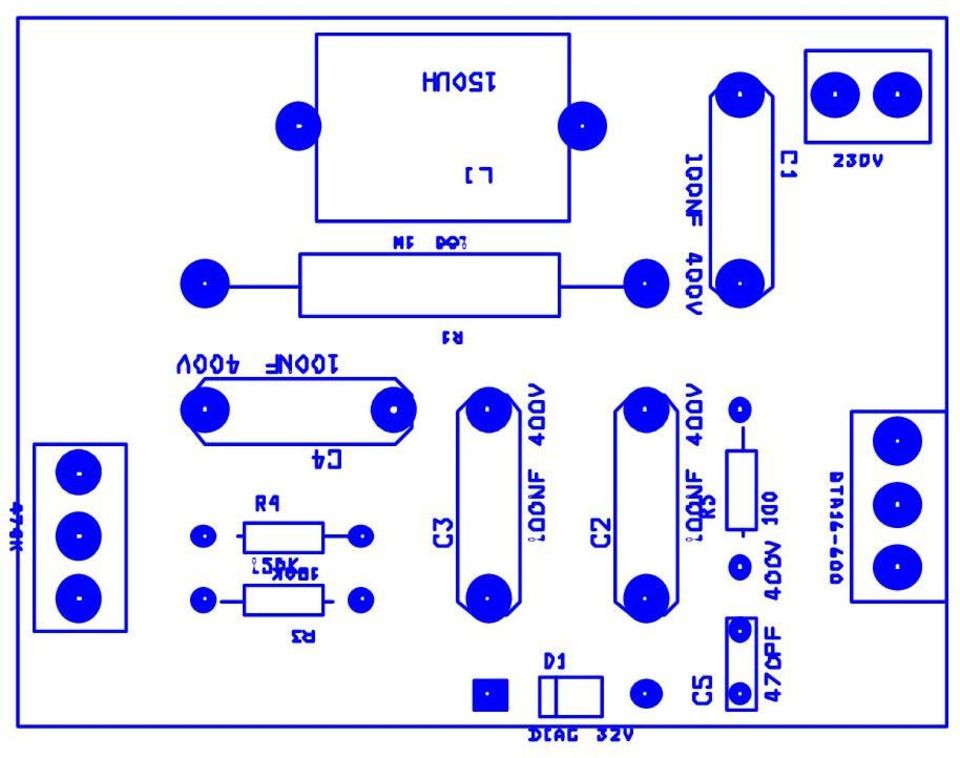
1 Réalisation de circuits imprimés EXTRA / 2002 Projet 3 - GRADATOR / Gradateur à TRIAC Projet : EXTRA1 Info : [DATA216] Révision : novembre 2000 Figure 3.1. Vue du circuit imprimé (images-composants\xx.jpg). 3.1 Liste des documents - Allure des principaux composants. - Prix du montage. - Schéma ORCAD ver 9.x. - Circuit imprimé LAYOUT. - Documentation du HEF4049B. 3.2 Liste des composants Tableau 3.3. Liste de composants (Projets-EXTRA1.xls / GRADATOR). No Quantité Référence Désignation Empreinte 1 4 C1,C2,C3,C4 100nF 400V C6PAS 2 1 C5 470pF 400V C6PAS 3 1 D1 DIAC 32V DO JP3 230V 2PL2 5 1 L1 150uH SELF Q1 BTA PL2 7 1 R W R14PAS 8 1 R2 470K 3PL2 9 1 R3 180K RC R4 150K RC R5 100 RC05 Thierry LEQUEU Novembre 2000 [DATA076] Fichier : PROJETS-EXTRA1.DOC Page 9

2 L1 JP V 2PL2 150uH SELF220 C1 100nF 400V C6PAS R4 150K RC05 R3 180K RC05 C2 100nF 400V C6PAs R2 470K 3PL2 D1 DIAC 32V DO41 C3 100nF 400V C6PAS R5 100 RC05 C5 470pF 400V CK Q1 BTA PL2 C4 100nF 400V C6PAS R W R14PAS Auteur : Thierry LEQUEU Size Document Number Rev A Gradateur 220 V / 500W 1 Date: Wednesday, November 22, 2000 Sheet 1 of 1

3
4

5 BTA12 BW/CW BTB12 BW/CW SNUBBERLESS TRIACS. FEATURES HIGH COMMUTATION : (di/dt)c > 12A/ms without snubber HIGH SURGE CURRENT : I TSM = 120A. V DRM UP TO 800V BTA Family : INSULATING VOLTAGE = 2500V (RMS) (UL RECOGNIZED : E81734) DESCRIPTION The BTA/BTB12 BW/CW triac family are high performance glass passivated chips technology. The SNUBBERLESS concept offer suppression of RC network and it is suitable for application such as phase control and static switching on inductive or resistive load. ABSOLUTE RATINGS (limiting values) A1 A2 G TO220AB (Plastic) Symbol Parameter Value Unit IT(RMS) ITSM RMS on-state current (360 conduction angle) Non repetitive surge peak on-state current ( Tj initial = 25 C ) BTA Tc = 85 C 12 A BTB Tc = 95 C tp = 8.3 ms 126 A tp = 10 ms 120 I2t I2t value tp = 10 ms 72 A2s di/dt Critical rate of rise of on-state current Gate supply : IG = 500mA dig/dt = 1A/µs Repetitive F = 50 Hz 20 A/µs Non Repetitive 100 Tstg Tj Storage and operating junction temperature range - 40 to to C C Tl Maximum lead temperature for soldering during 10 s at 4.5 mm from case 260 C Symbol Parameter BTA / BTB BW/CW Unit VDRM VRRM Repetitive peak off-state voltage Tj = 125 C V March /5
 A1 A2 G TO220AB (Plastic) Symbol Parameter Value Unit IT(RMS) ITSM RMS on-state current (360 conduction angle) Non repetitive surge peak on-state current ( Tj")
6 BTA12 BW/CW / BTB12 BW/CW THERMAL RESISTANCES Symbol Parameter Value Unit Rth (j-a) Junction to ambient 60 C/W Rth (j-c) DC Junction to case for DC BTA 3.3 C/W BTB 2.7 Rth (j-c) AC Junction to case for 360 conduction angle ( F= 50 Hz) BTA 2.5 C/W BTB 2.0 GATE CHARACTERISTICS (maximum values) PG (AV) =1W PGM = 10W (tp = 20 µs) IGM =4A(tp=20µs) VGM = 16V (tp = 20 µs). ELECTRICAL CHARACTERISTICS Symbol Test Conditions Quadrant Suffix Unit BW CW IGT VD=12V (DC) RL=33Ω Tj=25 C I-II-III MIN 2 1 ma MAX VGT VD=12V (DC) RL=33Ω Tj=25 C I-II-III MAX 1.5 V VGD VD=VDRM RL=3.3kΩ Tj=125 C I-II-III MIN 0.2 V tgt VD=VDRM IG = 500mA di G /dt = 3A/µs Tj=25 C I-II-III TYP 2 µs I L I G =1.2 I GT Tj=25 C I-III TYP 40 - ma II TYP 80 - I-III MAX - 50 II MAX - 80 I H * I T = 500mA gate open Tj=25 C MAX ma V TM * I TM = 17A tp= 380µs Tj=25 C MAX 1.60 V I DRM IRRM V DRM VRRM Rated Rated Tj=25 C MAX 0.01 ma Tj=125 C MAX 2 dv/dt * Linear slope up to V D =67%V DRM gate open Tj=125 C MIN V/µs TYP (di/dt)c * Without snubber Tj=125 C MIN A/ms * For either polarity of electrode A2 voltage with reference to electrode A1. TYP /5
 RL=33Ω Tj=25 C I-II-III MIN 2 1 ma MAX 50 35 VGT VD=12V (DC) RL=33Ω Tj=25 C I-II-III MAX 1.")
7 DB3 /DB4 / DC34 TRIGGER DIODES FEATURES VBO : 32V / 34V / 40V VERSIONS LOW BREAKOVER CURRENT DESCRIPTION High reliability glass passivation insuring parameter stability and protection against junction contamination. DO 35 (Glass) ABSOLUTE RATINGS (limiting values) Symbol Parameter Value Unit P Power dissipation on printed circuit (L = 10 mm) Ta = 65 C 150 mw I TRM Repetitive peak on-state current tp = 20 µs F= 100 Hz 2 A Tstg Tj Storage and operating junction temperature range - 40 to to +125 C C THERMAL RESISTANCES Symbol Parameter Value Unit R th (j-a) Junction to ambient 400 C/W Rth (j-l) Junction-leads 150 C/W April /4

8 DB3 / DB4 / DC34 ELECTRICAL CHARACTERISTICS (Tj = 25 C) Symbol Parameter Test Conditions Value Unit DB3 DC34 DB4 V BO Breakover voltage * C = 22nF ** see diagram 1 MIN V TYP MAX [I+VBOI-I-VBOI] Breakover voltage symmetry C = 22nF ** see diagram 1 MAX ± 3 V I V± I Dynamic breakover voltage * I =[I BO to I F =10mA] see diagram 1 MIN 5 V VO Output voltage * see diagram 2 MIN 5 V I BO Breakover current * C = 22nF ** MAX µa tr Rise time * see diagram 3 TYP 1.5 µs I B Leakage current * V B =0.5V BO max see diagram 1 * Electrical characteristic applicable in both forward and reverse directions. ** Connected in parallel with the devices. MAX 10 µa DIAGRAM 1 : Current-voltage characteristics DIAGRAM 2 : Test circuit for output voltage 10mA + I F 220 V 50 Hz 10 k 500 k 0.1 F D.U.T V O R = 20 -V I BO I B + V 0,5 V BO V V BO DIAGRAM 3 : Test circuit see diagram 2. Adjust R for lp=0.5a 90 % lp -I F 10 % tr 2/4

BTB04-600SL STANDARD 4A TRIAC MAIN FEATURES
 BTB-6SL STANDARD A TRIAC MAIN FEATURES A Symbol Value Unit I T(RMS) A V DRM /V RRM 6 V I GT(Q) ma G A A DESCRIPTION The BTB-6SL quadrants TRIAC is intended for general purpose applications where high surge
PINNING - TO220AB PIN CONFIGURATION SYMBOL
 BTA4 series GENERAL DESCRIPTION QUICK REFERENCE DATA Passivated triacs in a plastic envelope, SYMBOL PARAMETER MAX. MAX. UNIT intended for use in applications requiring high bidirectional transient and
Thyristor/Diode Modules M## 501 MCC MCD MDC
 Date: 29.9.214 Data Sheet Issue: 3 Absolute Maximum Ratings Thyristor/Diode Modules M## 51 VRRM VDRM [V] MCC MCD MDC 12 51-12io2 51-12io2 51-12io2 14 51-14io2 51-14io2 51-14io2 16 51-16io2 51-16io2 51-16io2
TIC225 SERIES SILICON TRIACS
 Copyright 200, Power Innovations Limited, UK JULY 975 - REVISED MARCH 200 Sensitive Gate Triacs 8 A RMS, 70 A Peak Glass Passivated Wafer 400 V to 800 V Off-State Voltage Max I GT of 5 ma (Quadrant ) MT
logic level for RCD/ GFI applications
 logic level for RCD/ GFI applications BT68 series GENERAL DESCRIPTION QUICK REFERENCE DATA Glass passivated, sensitive gate SYMBOL PARAMETER MAX. MAX. MAX. MAX. UNIT thyristors in a plastic envelope, intended
AN2703 Application note
 Application note list for SCRs, TRIACs, AC switches, and DIACS Introduction All datasheet parameters are rated as minimum or maximum values, corresponding to the product parameter distribution. In each
logic level for RCD/ GFI/ LCCB applications
 logic level for RCD/ GFI/ LCCB applications BT68W series GENERAL DESCRIPTION QUICK REFERENCE DATA Glass passivated, sensitive gate SYMBOL PARAMETER MAX. MAX. MAX. MAX. UNIT thyristors in a plastic envelope
I T(AV) off-state voltages. PINNING - TO92 variant PIN CONFIGURATION SYMBOL. 3 anode g
 off-state voltages. PINNING - TO92 variant PIN CONFIGURATION SYMBOL. 3 anode g") BT9 series GENERL DESCRIPTION QUICK REFERENCE DT Passivated, sensitive gate thyristors in a SYMBOL PRMETER MX. MX. MX. UNIT plastic envelope, intended for use in general purpose switching and phase BT9
BT9 series GENERL DESCRIPTION QUICK REFERENCE DT Passivated, sensitive gate thyristors in a SYMBOL PRMETER MX. MX. MX. UNIT plastic envelope, intended for use in general purpose switching and phase BT9
BTA40, BTA41 and BTB41 Series
 BTA4, BTA41 and BTB41 Series STANDARD 4A TRIACS Table 1: Main Features Symbol Value Unit I T(RMS) 4 A V DRM /V RRM 6 and 8 V I T (Q1 ) 5 ma DESCRIPTION Available in high power packages, the BTA/ BTB4-41
DISCRETE SEMICONDUCTORS DATA SHEET. BT151 series C Thyristors
 DISCRETE SEMICONDUCTORS DATA SHEET Product specification April 24 Product specification GENERAL DESCRIPTION QUICK REFERENCE DATA Passivated thyristors in a plastic SYMBOL PARAMETER MAX. MAX. MAX. UNIT
BTA12, BTB12, T12xx. 12 A Snubberless, logic level and standard triacs. Features. Applications. Order code. Description
 12 A Snubberless, logic level and standard triacs Features Medium current triac Low thermal resistance with clip bonding Low thermal resistance insulation ceramic for insulated BTA High commutation (4Q)
logic level for RCD/ GFI/ LCCB applications
 logic level for RCD/ GFI/ LCCB applications BT68GW GENERL DESCRIPTION QUICK REFERENCE DT Passivated, sensitive gate thyristor in a plastic SYMBOL PRMETER MX. UNIT envelope suitable for surface mounting,
(250 Volts Peak) SEMICONDUCTOR TECHNICAL DATA
 SEMICONDUCTOR TECHNICAL DATA") SEMICONDUCTOR TECHNICAL DATA Order this document by MOC00/D (0 Volts Peak) The MOC00 Series consists of gallium arsenide infrared emitting diodes, optically coupled to silicon bilateral switch and are
SEMICONDUCTOR TECHNICAL DATA Order this document by MOC00/D (0 Volts Peak) The MOC00 Series consists of gallium arsenide infrared emitting diodes, optically coupled to silicon bilateral switch and are
Schematic Mechanical Drawing Derating Curve. Input. Output. Product Catalogue
 Input 1 Product Catalogue Single Phase SSR (24VAC) 1 ~ 4 Amps : DC Control, : Triac output 42.5 Series : 1 J/K 3 Input (+) & 4 Input (-) 1 & 2 35.6 25.5 57.75 28. 45. A = 3.2 C/W B = 1. C/W C & D =.5 C/W
(250 Volts Peak) SEMICONDUCTOR TECHNICAL DATA
 SEMICONDUCTOR TECHNICAL DATA") SEMICONDUCTOR TECHNICAL DATA Order this document by MOC0/D (20 Volts Peak) The MOC0, MOC02 and MOC0 devices consist of gallium arsenide infrared emitting diodes optically coupled to a monolithic silicon
SEMICONDUCTOR TECHNICAL DATA Order this document by MOC0/D (20 Volts Peak) The MOC0, MOC02 and MOC0 devices consist of gallium arsenide infrared emitting diodes optically coupled to a monolithic silicon
BTW67 and BTW69 Series
 BTW67 and BTW69 Series STNDRD 50 SCRs MIN FETURES: Symbol Value Unit I T(RMS) 50 V DRM /V RRM 600 to 1200 V G K I GT 80 m G K DESCRIPTION vailable in high power packages, the BTW67 / BTW69 Series is suitable
MT..KB SERIES 55 A 90 A 110 A THREE PHASE CONTROLLED BRIDGE. Power Modules. Features. Description. Major Ratings and Characteristics
 MT..KB SERIES THREE PHASE CONTROLLED BRIDGE Power Modules Features Package fully compatible with the industry standard INT-A-pak power modules series High thermal conductivity package, electrically insulated
TISP4500H3BJ Overvoltage Protector
 *RoHS COMPLINT TISP4500H3BJ BIDIRECTIONL THYRISTOR OVERVOLTGE PROTECTORS TISP4500H3BJ Overvoltage Protector Non-Conductive During K.20/21/45 Power Contact Test - Off-State Voltage... >245 V rms - For Controlled
TISP4600F3, TISP4700F3 OBSOLETE
 *RoHS COMPLIANT TISP4600F3, TISP4700F3 HIGH OLTAGE BIDIRECTIONAL THYRISTOR OEROLTAGE PROTECTORS TISP4600F3, TISP4700F3 Ion-Implanted Breakdown Region Precise and Stable oltage Low oltage Overshoot under
SCR, 12 A, 15mA, 500 V, SOT78. Planar passivated SCR (Silicon Controlled Rectifier) in a SOT78 plastic package.
 in a SOT78 plastic package.") Rev. 5 2 March 29 Product data sheet 1. Product profile 1.1 General description Planar passivated SCR (Silicon Controlled Rectifier) in a SOT78 plastic package. 1.2 Features and benefits High reliability
Rev. 5 2 March 29 Product data sheet 1. Product profile 1.1 General description Planar passivated SCR (Silicon Controlled Rectifier) in a SOT78 plastic package. 1.2 Features and benefits High reliability
UNISONIC TECHNOLOGIES CO., LTD 50N06 Power MOSFET
 UNISONIC TECHNOLOGIES CO., LTD 50N06 50 Amps, 60 Volts N-CHANNEL POWER MOSFET DESCRIPTION TO-263 TO-25 The UTC 50N06 is three-terminal silicon device with current conduction capability of about 50A, fast
FLC21-135A LOW POWER FIRE LIGHTER CIRCUIT. Application Specific Discretes A.S.D.
 Application Specific iscretes A.S.. LC21-135A LOW POWER IRE LIGHTER CIRCUIT EATURES EICATE THYRISTOR STRUCTURE OR CAPACITIVE ISCHARGE IGNITION OPERATION HIGH PULSE CURRENT CAPABILITY I RM =90A @ tp=10µs
TISP9110LDM Overvoltage Protector
 *RoHS COMPLINT TISP9110LDM INTEGRTED COMPLEMENTRY BUFFERED-GTE SCRS FOR DUL POLRITY SLIC OEROLTGE PROTECTION TISP9110LDM Overvoltage Protector High Performance Protection for SLICs with +ve and -ve Battery
S101D01/S101D02 S201D01/S201D02
 S1D1/S1D/S1D1/S1D S1D1/S1D S1D1/S1D 1-Pin DIP Type SSR for Low Power Control Features 1. Compact ( 1-pin dual-in-line package type). RMS ON-state current I T : 1.Arms 3. Built-in zero-cross (S1D, S1D ).
Fundamental Characteristics of Thyristors
 A1001 Introduction The Thyristor family of semiconductors consists of several very useful devices. The most widely used of this family are silicon controlled rectifiers (SCRs), Triacs, SIDACs, and DIACs.
Item Symbols Conditions Ratings Units Repetitive peak reverse voltage VRRM - 600 V
 TS985C6R Low-Loss Fast Recovery Diode Maximum Rating and Characteristics Maximum ratings (at Ta=25 C unless otherwise specified.) Item Symbols Conditions Ratings Units Repetitive peak reverse voltage VRRM
Passivated, sensitive gate triacs in a SOT54 plastic package. General purpose switching and phase control
 TO-92 Rev. 9 9 November 2 Product data sheet. Product profile. General description Passivated, sensitive gate triacs in a SOT54 plastic package.2 Features and benefits Designed to be interfaced directly
C106 Series. Sensitive Gate Silicon Controlled Rectifiers
 C6 Series Sensitive Gate Silicon Controlled Rectifiers Reverse Blocking Thyristors Glassivated PNPN devices designed for high volume consumer applications such as temperature, light, and speed control;
NTE923 & NTE923D Integrated Circuit Precision Voltage Regulator
 NTE923 & NTE923D Integrated Circuit Precision Voltage Regulator Description: The NTE923 and NTE923D are voltage regulators designed primarily for series regulator applications. By themselves, these devices
5STP 06T1600 Old part no. T 906C-640-16
 Phase Control Thyristor Properties 5STP T1 Old part no. T 9C--1 Key Parameters High operational capability V DRM, V RRM = 1 V Possibility of serial and parallel connection I TAVm = 1 A Applications I TSM
(600 Volts Peak) SEMICONDUCTOR TECHNICAL DATA
 SEMICONDUCTOR TECHNICAL DATA") SEMICONDUCTOR TECHNICAL DATA Order this document by MOC0/D (00 Volts Peak) The MOC0, MOC02 and MOC0 devices consist of gallium arsenide infrared emitting diodes optically coupled to monolithic silicon
SEMICONDUCTOR TECHNICAL DATA Order this document by MOC0/D (00 Volts Peak) The MOC0, MOC02 and MOC0 devices consist of gallium arsenide infrared emitting diodes optically coupled to monolithic silicon
5STP 30T1800 Old part no. T 989C-3030-18
 Phase Control Thyristor Properties 5STP 3T18 Old part no. T 989C-33-18 Key Parameters High operational capability V DRM, V RRM = 1 8 V Possibility of serial and parallel connection I TAVm = 3 18 A Applications
5STP 21H4200 Old part no. TV 989-2100-42
 Phase Control Thyristor Properties 5STP 1H Old part no. T 989-1- Key Parameters High operational capability DRM, RRM = Possibility of serial and parallel connection I TAm = 19 A Applications I TSM = 3
MCR08B, MCR08M. Sensitive Gate Silicon Controlled Rectifiers. Reverse Blocking Thyristors. SCRs 0.8 AMPERES RMS 200 thru 600 VOLTS
 MCR8B, MCR8M Sensitive Gate Silicon Controlled Rectifiers Reverse Blocking Thyristors PNPN devices designed for line powered consumer applications such as relay and lamp drivers, small motor controls,
IRFP450. N - CHANNEL 500V - 0.33Ω - 14A - TO-247 PowerMESH MOSFET
 IRFP450 N - CHANNEL 500V - 0.33Ω - 14A - TO-247 PowerMESH MOSFET TYPE V DSS R DS(on) I D IRFP450 500 V < 0.4 Ω 14 A TYPICAL R DS(on) = 0.33 Ω EXTREMELY HIGH dv/dt CAPABILITY 100% AVALANCHE TESTED VERY
10MQ100N SCHOTTKY RECTIFIER. I F(AV) = 2.1Amp V R = 100V. Bulletin PD-20520 rev. M 07/04. Major Ratings and Characteristics. Description/ Features
 = 2.1Amp V R = 100V. Bulletin PD-20520 rev. M 07/04. Major Ratings and Characteristics. Description/ Features") 0MQ00N SCHOTTKY RECTIFIER 2. Amp I F(AV) = 2.Amp V R = 00V Major Ratings and Characteristics Characteristics 0MQ00N Units I F DC 2. A V RRM 00 V I FSM @ tp = 5 µs sine 20 A V F @.5Apk, T =25 C 0.68 V J
0MQ00N SCHOTTKY RECTIFIER 2. Amp I F(AV) = 2.Amp V R = 00V Major Ratings and Characteristics Characteristics 0MQ00N Units I F DC 2. A V RRM 00 V I FSM @ tp = 5 µs sine 20 A V F @.5Apk, T =25 C 0.68 V J
Features. Symbol JEDEC TO-220AB
 Data Sheet June 1999 File Number 2253.2 3A, 5V,.4 Ohm, N-Channel Power MOSFET This is an N-Channel enhancement mode silicon gate power field effect transistor designed for applications such as switching
IRF150 [REF:MIL-PRF-19500/543] 100V, N-CHANNEL. Absolute Maximum Ratings
![IRF150 [REF:MIL-PRF-19500/543] 100V, N-CHANNEL. Absolute Maximum Ratings](/thumbs/40/21333646.jpg "IRF150 [REF:MIL-PRF-19500/543] 100V, N-CHANNEL. Absolute Maximum Ratings") PD - 90337G REPETITIVE AVALANCHE AND dv/dt RATED HEXFET TRANSISTORS THRU-HOLE (TO-204AA/AE) Product Summary Part Number BVDSS RDS(on) ID IRF150 100V 0.055Ω 38A IRF150 JANTX2N6764 JANTXV2N6764 [REF:MIL-PRF-19500/543]
PD - 90337G REPETITIVE AVALANCHE AND dv/dt RATED HEXFET TRANSISTORS THRU-HOLE (TO-204AA/AE) Product Summary Part Number BVDSS RDS(on) ID IRF150 100V 0.055Ω 38A IRF150 JANTX2N6764 JANTXV2N6764 [REF:MIL-PRF-19500/543]
STP6N60FI N - CHANNEL ENHANCEMENT MODE POWER MOS TRANSISTOR
 N - CHANNEL ENHANCEMENT MODE POWER MOS TRANSISTOR TYPE VDSS RDS(on) ID STP6N60FI 600 V < 1.2 Ω 3.8 A TYPICAL R DS(on) =1Ω AVALANCHE RUGGED TECHNOLOGY 100% AVALANCHE TESTED REPETITIVE AVALANCHE DATA AT
IRF830. N - CHANNEL 500V - 1.35Ω - 4.5A - TO-220 PowerMESH MOSFET
 IRF830 N - CHANNEL 500V - 1.35Ω - 4.5A - TO-220 PowerMESH MOSFET TYPE V DSS R DS(on) I D IRF830 500 V < 1.5 Ω 4.5 A TYPICAL R DS(on) = 1.35 Ω EXTREMELY HIGH dv/dt CAPABILITY 100% AVALANCHE TESTED VERY
BT139B-600. 1. General description. 2. Features and benefits. 3. Applications. Quick reference data. 4Q Triac 27 September 2013 Product data sheet
 D2PAK 27 September 213 Product data sheet 1. General description Planar passivated four quadrant triac in a SOT44 (D2PAK) surface-mountable plastic package intended for use in applications requiring high
0.185 (4.70) 0.170 (4.31) 0.055 (1.39) 0.045 (1.14) Features 0.603 (15.32) 0.573 (14.55) 0.104 (2.64) 0.094 (2.39)
 0.170 (4.31) 0.055 (1.39) 0.045 (1.14) Features 0.603 (15.32) 0.573 (14.55) 0.104 (2.64) 0.094 (2.39)") *.6 (4.6).9 (2.28).25 (5.2).9 (4.83).45 (.54) Max..4 (.4).35 (8.89).54 (3.9).42 (3.6) ia. PIN S.48 (29.6).8 (28.4) * May be notched or flat.3 (2.87).2 (2.56).635 (6.3).58 (4.73).37 (.94).26 (.66).5 (2.67).95
*.6 (4.6).9 (2.28).25 (5.2).9 (4.83).45 (.54) Max..4 (.4).35 (8.89).54 (3.9).42 (3.6) ia. PIN S.48 (29.6).8 (28.4) * May be notched or flat.3 (2.87).2 (2.56).635 (6.3).58 (4.73).37 (.94).26 (.66).5 (2.67).95
CoolMOS TM Power Transistor
 CoolMOS TM Power Transistor Features New revolutionary high voltage technology Intrinsic fast-recovery body diode Extremely low reverse recovery charge Ultra low gate charge Extreme dv /dt rated Product
CA723, CA723C. Voltage Regulators Adjustable from 2V to 37V at Output Currents Up to 150mA without External Pass Transistors. Features.
 CA73, CA73C Data Sheet April 1999 File Number 788. Voltage Regulators Adjustable from V to 37V at Output Currents Up to 1mA without External Pass Transistors The CA73 and CA73C are silicon monolithic integrated
ACTP250J1BJ AC Transient Protector
 *RoHS COMPLIANT ACTP250J1BJ BIDIRECTIONAL THYRISTOR OVERVOLTAGE PROTECTORS ACTP250J1BJ AC Transient Protector Designed to withstand a 2.5 kv (1.2/50 voltage, 8/20 current) combination wave surge per IEC
Power MOSFET FEATURES. IRF520PbF SiHF520-E3 IRF520 SiHF520. PARAMETER SYMBOL LIMIT UNIT Drain-Source Voltage V DS 100 V Gate-Source Voltage V GS ± 20
 Power MOSFET PRODUCT SUMMARY (V) 100 R DS(on) ( ) = 0.7 Q g (Max.) (nc) 16 Q gs (nc) 4.4 Q gd (nc) 7.7 Configuration Single TO0AB G DS ORDERING INFORMATION Package Lead (Pb)free SnPb G D S NChannel MOSFET
www.jameco.com 1-800-831-4242
 Distributed by: www.jameco.com 1-800-831-4242 The content and copyrights of the attached material are the property of its owner. LF411 Low Offset, Low Drift JFET Input Operational Amplifier General Description
BT138-600E. 1. General description. 2. Features and benefits. 3. Applications. Quick reference data. 4Q Triac 30 August 2013 Product data sheet
 TO-22AB 3 August 213 Product data sheet 1. General description Planar passivated sensitive gate four quadrant triac in a SOT78 (TO-22AB) plastic package intended for use in general purpose bidirectional
IRLR8729PbF IRLU8729PbF
 Applications l High Frequency Synchronous Buck Converters for Computer Processor Power l High Frequency Isolated DC-DC Converters with Synchronous Rectification for Telecom and Industrial Use Benefits
ACS108. Overvoltage protected AC switch (ACS ) Description. Features. Applications
 Description. Features. Applications") Overvoltage protected AC switch (ACS ) Datasheet - production data OUT G TO-92-6SA -8SA COM COM OUT COMG -6SN -8SN Description The belongs to the AC switch range (built with A. S. D. technology). This
Overvoltage protected AC switch (ACS ) Datasheet - production data OUT G TO-92-6SA -8SA COM COM OUT COMG -6SN -8SN Description The belongs to the AC switch range (built with A. S. D. technology). This
38 Series - Relay interface modules 0.1-2 - 3-5 - 6-8 A
 38 Series - Relay interface modules 0.1-2 - 3-5 - 6-8 A Common features Instant ejection of relay by plastic retaining clip Integral coil indication and protection circuit EMR Electromechanical Relays
General purpose low power phase control General purpose low power switching Solid-state relay. Symbol Parameter Conditions Min Typ Max Unit V DRM
 TO-92 May 25 Product data sheet. General description Planar passivated very sensitive gate four quadrant triac in a SOT54 plastic package intended to be interfaced directly to microcontrollers, logic integrated
STP62NS04Z N-CHANNEL CLAMPED 12.5mΩ - 62A TO-220 FULLY PROTECTED MESH OVERLAY MOSFET
 N-CHANNEL CLAMPED 12.5mΩ - 62A TO-220 FULLY PROTECTED MESH OVERLAY MOSFET TYPE V DSS R DS(on) I D STP62NS04Z CLAMPED
Dual Common-Cathode Ultrafast Plastic Rectifier
 (F,B)6AT thru (F,B)6JT Dual Common-Cathode Ultrafast Plastic Rectifier TO-0AB 6xT PIN PIN 3 PIN CASE 3 TO-63AB ITO-0AB F6xT PIN PIN 3 PIN 3 FEATURES Glass passivated chip junction Ultrafast recovery time
Characteristics Values Units. Rectangular waveform 0.5 A. range - 55 to 150 C
 Bulletin I075 rev. C 05/06 IR0530CSPTRPbF 0.5 Amp 30 Volt Features Ultra Low V F To Footprint Area Very Low Profile (
AUTOMOTIVE MOSFET. C Soldering Temperature, for 10 seconds 300 (1.6mm from case )
") PD 9399A AUTOMOTIVE MOSFET Typical Applications Electric Power Steering (EPS) Antilock Braking System (ABS) Wiper Control Climate Control Power Door Benefits Advanced Process Technology Ultra Low OnResistance
PD 9399A AUTOMOTIVE MOSFET Typical Applications Electric Power Steering (EPS) Antilock Braking System (ABS) Wiper Control Climate Control Power Door Benefits Advanced Process Technology Ultra Low OnResistance
38 Series - Relay interface modules 0.1-2 - 3-5 - 6-8 - 16 A
 38 Series - Relay interface modules 0.1-2 - 3-5 - 6-8 - 16 A 38 SERIES Common features Instant ejection of relay by plastic retaining clip Integral coil indication and protection circuit EMR Electromechanical
38 SERIES. Relay interface modules 0.1-2 - 3-5 - 6-8 - 16 A. EMR Electromechanical Relays. Common features. SSR Solid State Relays. 6.
 38 Relay interface modules 0.1-2 - 3-5 - 6-8 - 16 A 38 Common features Instant ejection of relay by plastic retaining clip Integral coil indication and protection circuit 6.2 mm wide EMR - DC, AC or AC/DC
8ETH06 8ETH06S 8ETH06-1 8ETH06FP
 Bulletin PD-0746 rev. D 03/03 8ETH06 8ETH06S 8ETH06-8ETH06FP Hyperfast Rectifier Features Hyperfast Recovery Time Low Forward Voltage Drop Low Leakage Current 75 C Operating unction Temperature UL E78996
DATA SHEET. TDA8560Q 2 40 W/2 Ω stereo BTL car radio power amplifier with diagnostic facility INTEGRATED CIRCUITS. 1996 Jan 08
 INTEGRATED CIRCUITS DATA SHEET power amplifier with diagnostic facility Supersedes data of March 1994 File under Integrated Circuits, IC01 1996 Jan 08 FEATURES Requires very few external components High
STW34NB20 N-CHANNEL 200V - 0.062 Ω - 34A TO-247 PowerMESH MOSFET
 N-CHANNEL 200V - 0.062 Ω - 34A TO-247 PowerMESH MOSFET Table 1. General Features Figure 1. Package Type V DSS R DS(on) I D STW34NB20 200 V < 0.075 Ω 34 A FEATURES SUMMARY TYPICAL R DS(on) = 0.062 Ω EXTREMELY
TDA4605 CONTROL CIRCUIT FOR SWITCH MODE POWER SUPPLIES USING MOS TRANSISTORS
 CONTROL CIRCUIT FOR SWITCH MODE POWER SUPPLIES USING MOS TRANSISTORS Fold-Back Characteristic provides Overload Protection for External Diodes Burst Operation under Short-Circuit and no Load Conditions
Power MOSFET. IRF9520PbF SiHF9520-E3 IRF9520 SiHF9520. PARAMETER SYMBOL LIMIT UNIT Drain-Source Voltage V DS - 100 V Gate-Source Voltage V GS ± 20
 Power MOSFET PRODUCT SUMMARY (V) 100 R DS(on) ( ) = 10 V 0.60 Q g (Max.) (nc) 18 Q gs (nc) 3.0 Q gd (nc) 9.0 Configuration Single TO220AB G DS ORDERING INFORMATION Package Lead (Pb)free SnPb G S D PChannel
Trench gate field-stop IGBT, M series 650 V, 10 A low loss. Features. Description
 Trench gate field-stop IGBT, M series 650 V, 10 A low loss Datasheet - production data TAB D2PAK 1 3 Features 6 µs of short-circuit withstand time VCE(sat) = 1.55 V (typ.) @ IC = 10 A Tight parameter distribution
STP10NK60Z/FP, STB10NK60Z/-1 STW10NK60Z N-CHANNEL 600V-0.65Ω-10A TO-220/FP/D 2 PAK/I 2 PAK/TO-247 Zener-Protected SuperMESH Power MOSFET
 STP10NK60Z/FP, STB10NK60Z/-1 STW10NK60Z N-CHANNEL 600V-0.65Ω-10A TO-220/FP/D 2 PAK/I 2 PAK/TO-247 Zener-Protected SuperMESH Power MOSFET TYPE V DSS R DS(on) I D Pw STP10NK60Z STP10NK60ZFP STB10NK60Z STB10NK60Z-1
STB4NK60Z, STB4NK60Z-1, STD4NK60Z STD4NK60Z-1, STP4NK60Z,STP4NK60ZFP
 STB4NK60Z, STB4NK60Z-1, STD4NK60Z STD4NK60Z-1, STP4NK60Z,STP4NK60ZFP N-channel 600 V - 1.76 Ω - 4 A SuperMESH Power MOSFET DPAK - D 2 PAK - IPAK - I 2 PAK - TO-220 - TO-220FP Features Type V DSS R DS(on)
BUZ11. 30A, 50V, 0.040 Ohm, N-Channel Power MOSFET. Features. [ /Title (BUZ1 1) /Subject. (30A, 50V, 0.040 Ohm, N- Channel. Ordering Information
 /Subject. (30A, 50V, 0.040 Ohm, N- Channel. Ordering Information") Data Sheet June 1999 File Number 2253.2 [ /Title (BUZ1 1) /Subject (3A, 5V,.4 Ohm, N- Channel Power MOS- FET) /Autho r () /Keywords (Intersil Corporation, N- Channel Power MOS- FET, TO- 22AB ) /Creator
Data Sheet June 1999 File Number 2253.2 [ /Title (BUZ1 1) /Subject (3A, 5V,.4 Ohm, N- Channel Power MOS- FET) /Autho r () /Keywords (Intersil Corporation, N- Channel Power MOS- FET, TO- 22AB ) /Creator
STP6NK60Z - STP6NK60ZFP STB6NK60Z - STB6NK60Z-1 N-CHANNEL 600V - 1Ω - 6A TO-220/TO-220FP/D 2 PAK/I 2 PAK Zener-Protected SuperMESH Power MOSFET
 STP6NK60Z - STP6NK60ZFP STB6NK60Z - STB6NK60Z-1 N-CHANNEL 600V - 1Ω - 6A TO-220/TO-220FP/D 2 PAK/I 2 PAK Zener-Protected SuperMESH Power MOSFET TYPE V DSS R DS(on) I D Pw STP6NK60Z STP6NK60ZFP STB6NK60Z
L293B L293E PUSH-PULL FOUR CHANNEL DRIVERS. OUTPUT CURRENT 1A PER CHANNEL PEAK OUTPUT CURRENT 2A PER CHANNEL (non repetitive) INHIBIT FACILITY
 INHIBIT FACILITY") L293B L293E PUSH-PULL FOUR CHANNEL DRIVERS OUTPUT CURRENT 1A PER CHANNEL PEAK OUTPUT CURRENT 2A PER CHANNEL (non repetitive) INHIBIT FACILITY. HIGH NOISE IMMUNITY SEPARATE LOGIC SUPPLY OVERTEMPERATURE
L293B L293E PUSH-PULL FOUR CHANNEL DRIVERS OUTPUT CURRENT 1A PER CHANNEL PEAK OUTPUT CURRENT 2A PER CHANNEL (non repetitive) INHIBIT FACILITY. HIGH NOISE IMMUNITY SEPARATE LOGIC SUPPLY OVERTEMPERATURE
High Efficiency Thyristor
 LE2HB High Efficiency hyristor 2 M.4 Single hyristor Part number LE2HB Backside: anode 2 Features / dvantages: pplications: Package: O-247 hyristor for line frequency Planar passivated chip Long-term stability
C Soldering Temperature, for 10 seconds 300 (1.6mm from case )
") l Advanced Process Technology l Ultra Low On-Resistance l Dynamic dv/dt Rating l 75 C Operating Temperature l Fast Switching l Fully Avalanche Rated l Optimized for SMPS Applications Description Advanced
l Advanced Process Technology l Ultra Low On-Resistance l Dynamic dv/dt Rating l 75 C Operating Temperature l Fast Switching l Fully Avalanche Rated l Optimized for SMPS Applications Description Advanced
1 Form A Solid State Relay
 Form A Solid State Relay VOAT, VOAABTR FEATURES 9 S S DC S' 3 S' High speed SSR - t on /t off < 8 μs Maximum R ON. Isolation test voltage 3 V RMS Load voltage V Load current A DC configuration DIP- package
S112-XHS. Description. Features. Agency Approvals. Applications. Absolute Maximum Ratings. Schematic Diagram. Ordering Information
 Description Features The S112-X is a bi-directional, single-pole, single-throw, normally open multipurpose solid-state relay. The circuit is composed of one input IR LED with a series limiting resistor
STPS40L15CW. 2 x 20 Amps SCHOTTKY RECTIFIER. Case Styles. I F(AV) = 40Amp V R = 15V. Bulletin PD-20622 rev. B 10/06. Description/ Features
 = 40Amp V R = 15V. Bulletin PD-20622 rev. B 10/06. Description/ Features") Bulletin PD-20622 rev. B 0/06 STPS40L5CW SCHOTTKY RECTIFIER 2 x 20 Amps I F(AV) = 40Amp V R = 5V Major Ratings and Characteristics Characteristics Values Units I F(AV) Rectangular 40 A waveform V RRM 5
Bulletin PD-20622 rev. B 0/06 STPS40L5CW SCHOTTKY RECTIFIER 2 x 20 Amps I F(AV) = 40Amp V R = 5V Major Ratings and Characteristics Characteristics Values Units I F(AV) Rectangular 40 A waveform V RRM 5
NEW TRIACS: IS THE SNUBBER CIRCUIT NECESSARY?
 APPLICATION NOTE NEW TRIACS: IS THE SNUBBER CIRCUIT NECESSARY? T. Castagnet When driving an inductive load, triacs are designed with RC snubber. These commutation aid networks are badly optimized in most
N-channel enhancement mode TrenchMOS transistor
 FEATURES SYMBOL QUICK REFERENCE DATA Trench technology d V DSS = V Low on-state resistance Fast switching I D = A High thermal cycling performance Low thermal resistance R DS(ON) mω (V GS = V) g s R DS(ON)
.OPERATING SUPPLY VOLTAGE UP TO 46 V
 L298 DUAL FULL-BRIDGE DRIVER.OPERATING SUPPLY VOLTAGE UP TO 46 V TOTAL DC CURRENT UP TO 4 A. LOW SATURATION VOLTAGE OVERTEMPERATURE PROTECTION LOGICAL "0" INPUT VOLTAGE UP TO 1.5 V (HIGH NOISE IMMUNITY)
S102S02 Series S202S02 Series
 SS Series Non-zero cross type is also available. (SS1 Series/ SS1 Series) IT(rms) A, Zero Cross type SIP pin Triac output SSR Description SS Series and Solid State Relays (SSR) are an integration of an
TDA2040. 20W Hi-Fi AUDIO POWER AMPLIFIER
 20W Hi-Fi AUDIO POWER AMPLIFIER DESCRIPTION The TDA2040 is a monolithic integrated circuit in Pentawatt package, intended for use as an audio class AB amplifier. Typically it provides 22W output power
High Performance Schottky Rectifier, 1 A
 High Performance Schottky Rectifier, A VS-MQNPbF Cathode Anode DO-24AC (SMA) PRODUCT SUMMARY Package DO-24AC (SMA) I F(AV) A V R V V F at I F.78 V I RM ma at 25 C T J max. 5 C Diode variation Single die
TISP6NTP2C High Voltage Ringing SLIC Protector
 *RoHS COMPLINT TISP6NTP2C QUD FORWRD-CONDUCTING P-GTE THYRISTORS PROGRMMBLE OVERVOLTGE PROTECTORS TISP6NTP2C High Voltage Ringing SLIC Protector Independent Tracking Overvoltage Protection for Two SLICs:
High-speed switching diodes. Type number Package Configuration Package NXP JEITA JEDEC
 Rev. 8 18 November 2010 Product data sheet 1. Product profile 1.1 General description, encapsulated in small Surface-Mounted Device (SMD) plastic packages. Table 1. Product overview Type number Package
STPS20L15DPbF SCHOTTKY RECTIFIER. Case Styles. I F(AV) = 20Amp V R = 15V. Bulletin PD-20873 rev. A 02/07. Major Ratings and Characteristics
 = 20Amp V R = 15V. Bulletin PD-20873 rev. A 02/07. Major Ratings and Characteristics") STPS20L5DPbF SCHOTTKY RECTIFIER 20 Amps I F(AV) = 20Amp V R = 5V Major Ratings and Characteristics Characteristics Values Units I F(AV) Rectangular 20 A waveform V RRM 5 V I FSM @ tp = 5 μs sine 700 A
STPS20L5DPbF SCHOTTKY RECTIFIER 20 Amps I F(AV) = 20Amp V R = 5V Major Ratings and Characteristics Characteristics Values Units I F(AV) Rectangular 20 A waveform V RRM 5 V I FSM @ tp = 5 μs sine 700 A
TOSHIBA Insulated Gate Bipolar Transistor Silicon N Channel IGBT GT60J323
 GT6J2 TOSHIBA Insulated Gate Bipolar Transistor Silicon N Channel IGBT GT6J2 Current Resonance Inverter Switching Application Unit: mm Enhancement mode type High speed : t f =.6 μs (typ.) (I C = 6A) Low
TDA1085C. http://onsemi.com MARKING DIAGRAM ORDERING INFORMATION. Figure 1. Representative Block Diagram and Pin Connections AWLYYWW
 The TDA1085C is a phase angle triac controller having all the necessary functions for universal motor speed control in washing machines. It operates in closed loop configuration and provides two ramp possibilities.
TSM2N7002K 60V N-Channel MOSFET
 SOT-23 SOT-323 Pin Definition: 1. Gate 2. Source 3. Drain PRODUCT SUMMARY V DS (V) R DS(on) (Ω) I D (ma) 5 @ V GS = 10V 100 60 5.5 @ V GS = 5V 100 Features Low On-Resistance ESD Protection High Speed Switching
SMD version of BUK118-50DL
 DESCRIPTION QUICK REFERENCE DT Monolithic temperature and SYMBOL PRMETER MX. UNIT overload protected logic level power MOSFET in TOPFET2 technology V DS Continuous drain source voltage 50 V assembled in
TPI. Tripolar protection for ISDN interfaces. Features. Description. Complies with following standards. Benefits
 Tripolar protection for ISDN interfaces Features Bidirectional triple crowbar protection Peak pulse current: I PP = 30, 10/1000 µs Breakdown voltage: TPI80N: 80 V TPI120N: 120 V vailable in SO-8 package
MUR1520 MURB1520 MURB1520-1
 MUR520 MURB520 MURB520- Ultrafast Rectifier Features Ultrafast Recovery Time Low Forward Voltage Drop Low Leakage Current 75 C Operating Junction Temperature t rr = 35ns I F(AV) = 5Amp V R = 200V Description/
PDS5100H. Product Summary. Features and Benefits. Mechanical Data. Description and Applications. Ordering Information (Note 5) Marking Information
 Marking Information") Green 5A HIGH VOLTAGE SCHOTTKY BARRIER RECTIFIER POWERDI 5 Product Summary I F V R V F MAX (V) I R MAX (ma) (V) (A) @ +25 C @ +25 C 1 5..71.35 Description and Applications This Schottky Barrier Rectifier
Green 5A HIGH VOLTAGE SCHOTTKY BARRIER RECTIFIER POWERDI 5 Product Summary I F V R V F MAX (V) I R MAX (ma) (V) (A) @ +25 C @ +25 C 1 5..71.35 Description and Applications This Schottky Barrier Rectifier
D-PAK version of BUK117-50DL
 D-PK version of BUK117-50DL DESCRIPTION QUICK REFERENCE DT Monolithic temperature and SYMBOL PRMETER MX. UNIT overload protected logic level power MOSFET in TOPFET2 technology V DS Continuous drain source
Schottky Rectifier, 100 A
 Schottky Rectifier, A VS-BGQ Cathode Anode PowerTab PRODUCT SUMMARY Package PowerTab I F(AV) A V R V V F at I F 0.82 V I RM 180 ma at 125 C T J max. 175 C Diode variation Single die E AS 9 mj FEATURES
SMPS MOSFET. V DSS R DS (on) max I D
 max I D") Applications l Switch Mode Power Supply (SMPS) l Uninterruptable Power Supply l High speed power switching SMPS MOSFET PD 93773A IRF820A HEXFET Power MOSFET V DSS R DS (on) max I D 500V 3.0Ω 2.5A Benefits
Applications l Switch Mode Power Supply (SMPS) l Uninterruptable Power Supply l High speed power switching SMPS MOSFET PD 93773A IRF820A HEXFET Power MOSFET V DSS R DS (on) max I D 500V 3.0Ω 2.5A Benefits
200V, N-CHANNEL. Absolute Maximum Ratings. Features: www.irf.com 1 PD - 90370
 PD - 90370 REPETITIVE AVALANCHE AND dv/dt RATED HEXFET TRANSISTORS THRU-HOLE (TO-204AA/AE) IRF240 200V, N-CHANNEL Product Summary Part Number BVDSS RDS(on) ID IRF240 200V 0.18Ω 18A The HEXFET technology
Projet 5 - K3501 / Onduleur 12V DC - 220V AC.
 Thierry LEQUEU Septembre 26 [DATA76] Fichier : PROJETS-IUT1.DOC Projet 5 - K351 / Onduleur 12V DC - 22V AC. Projet : PROJETS-IUT1 Info : kit Velleman, [DATA12]. Révision : 24 janvier 2 5.1 Liste des documents
How To Test A Sidactor Series For A Power Supply
 SDP Series - SOT23-5 RoHS Pb e3 Description This new SIDACtor series is targeted for the tertiary or line driver side protection position for VDSL2+, ADSL2 applications and general I/O protection functions.
IR2117(S)/IR2118(S) & (PbF)
/IR2118(S) & (PbF)") Data Sheet No. PD14 Rev N IR2117(S)/IR211(S) & (PbF) Features Floating channel designed for bootstrap operation Fully operational to +V Tolerant to negative transient voltage dv/dt immune Gate drive supply
Data Sheet No. PD14 Rev N IR2117(S)/IR211(S) & (PbF) Features Floating channel designed for bootstrap operation Fully operational to +V Tolerant to negative transient voltage dv/dt immune Gate drive supply
TL783C, TL783Y HIGH-VOLTAGE ADJUSTABLE REGULATOR
 HIGH-VOLTAGE USTABLE REGULATOR SLVS36C SEPTEMBER 1981 REVISED APRIL 1997 Output Adjustable From 1.25 V to 125 V When Used With an External Resistor Divider 7-mA Output Current Full Short-Circuit, Safe-Operating-Area,
Lower Conduction Losses Low Thermal Resistance to PCB ( 0.5 C/W)
") PD -97428 IRFH5020PbF HEXFET Power MOSFET V DS 200 V 55 m: R DS(on) max (@V GS = V) Q g (typical) 36 nc R G (typical).9 : I D (@T c(bottom) = 25 C) 43 A PQFN 5X6 mm Applications Secondary Side Synchronous
PD -97428 IRFH5020PbF HEXFET Power MOSFET V DS 200 V 55 m: R DS(on) max (@V GS = V) Q g (typical) 36 nc R G (typical).9 : I D (@T c(bottom) = 25 C) 43 A PQFN 5X6 mm Applications Secondary Side Synchronous
STGW40NC60V N-CHANNEL 50A - 600V - TO-247 Very Fast PowerMESH IGBT
 N-CHANNEL 50A - 600V - TO-247 Very Fast PowerMESH IGBT Table 1: General Features STGW40NC60V 600 V < 2.5 V 50 A HIGH CURRENT CAPABILITY HIGH FREQUENCY OPERATION UP TO 50 KHz LOSSES INCLUDE DIODE RECOVERY