GETTING STARTED WITH PROGRAMMABLE LOGIC DEVICES, THE 16V8 AND 20V8
|
|
|
- Georgiana Lindsey
- 9 years ago
- Views:
Transcription
1 GETTING STARTED WITH PROGRAMMABLE LOGIC DEVICES, THE 16V8 AND 20V8 Robert G. Brown All Rights Reserved August 25, 2000 Alta Engineering 58 Cedar Lane New Hartford, CT (860)
 489-8003")
2 Hands on Design with Programmable Logic Devices The introduction of programmable logic devices (PLDs) was a great boon to the field of digital hardware design. The second generation PLD, the GAL (which stands for Generic Array Logic, a trademark of Lattice Semiconductor) is particularly suited for the small scale hardware designer. GALs offer the following benefits to the hardware designer: Flexibility - GALs are very flexible devices, they can implement both combinatorial logic functions (AND, OR, NAND etc.) and registered logic functions (counters, shift registers etc.) on the same chip. PAL replacement- The GAL16V8 and GAL20V8 each can directly replace over 20 of the common PAL (Programmable Array Logic - the first generation PLD) types each. This means you only need to stock 2 GAL types to handle your PLD needs. Space savings - In my experience each GAL has typically replaced between 2 and 4 standard TTL chips, saving a large amount of board space. Speed - GALs are fast devices with propagation delay down as low as 7 ns. Typical GALs have a propagation delay of only 15 ns - faster then standard 7400 or 74LS series logic. Reprogrammability - Not only are GALs programmable giving the ability to correct design errors and make board layout easier, they can be reprogrammed up to 100 times. Erasing and programming takes only a few seconds. Cost - In addition to the savings in PC board real estate, standard speed GAL16V8s and GAL20V8s (25 and 15 ns) cost only a few dollars even in small quantities. There are several varieties of GALs but I will limit this article to the GAL16V8 and GAL20V8. They are easy to design with and are the least expensive and most readily available GAL devices. Rather then get bogged down with the internal details of the devices, we'll cover what is needed to use these PLDs in your designs and then look at a real life design example. The Device Architecture The GAL16V8 is commonly packaged in a standard 20 pin DIP and the GAL20V8 is commonly packaged in a 24 pin skinny DIP (a 24 pin skinny DIP is 0.3 inches wide, the same width as a 20 pin DIP and half the width of a standard 24 pin DIP). The pinout for both devices is shown in figure 1. For the GAL16V8 pin 10 is the ground pin and pin 20 the +5 volt pin (VCC). Pins 12 through 19 are each connected to Output Logic Macro Cells (OLMC). The OLMC allows these pins to act as inputs, combinatorial outputs, registered outputs and input/output pins. Pins 2 through 9 are always general purpose input pins. If any of the OLMC are configured as registered outputs then pin 1 is a Clock input and pin 11 is the Output Enable for the registered outputs. If none of the OLMC 2
 and registered logic functions (counters, shift registers etc.) on the same chip.")
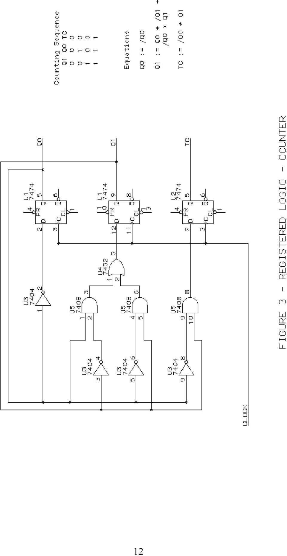
3 are registered then pins 1 and 11 are general purpose inputs. Internal to the chip is an array of and/or logic that is configured with each OLMC when the chip is programmed. The 20V8 has a similar design, the main difference from the 16V8 is the four additional input pins. The Design Tools In addition to your PC you will need only three tools to do design work with PLDs, a text editor, a logic compiler and a device programmer. A logic compiler is a program that translates a high level design file, in which the relationship between inputs and outputs is expressed in the form of equations, to a low level file device specific file for the programmer. The low level file used by the programmer is called a JEDEC file and is sometimes referred to as a 'fuse map'. (Earlier PLDs were programmed by literally blowing up fuses internal to the device leaving only the desired connections - of course they could not be reprogrammed - you threw away your mistakes.) National Semiconductor used to offer a FREE logic compiler before they got out of the PLD business. You can still get a copy of their PLAN logic compiler off of the Alta Engineering web site at The high level design file for PLAN is called an equation file and uses the extension.eqn, the output JEDEC file uses the extension.jed. Since PLAN is available to everyone I will use it in the examples, the concepts however are universal, not specific to PLAN. The equation file is a standard ASCII text file and can be produced using any text editor. Designing with Equations If you normally design with standard TTL devices, shifting to design using GALs might take a slight adjustment. However the underlying concepts are the same. In the equations a + is used to represent OR, a * to represent AND a / for NOT or inversion. In figure 2a show the equation represent by an AND gate. Each group of signals ANDed together is referred to as a product term. Figure 2b shows the equivalent representation for a two input OR gate. In figure 2c a more complicated piece of logic is represented, it includes the use of the / symbol to show inversion. Notice how the equation is organized. The equations are written in a sum of products format, a useful convention is to list each product term on a separate line. The inversion can also occur on the output as shown is in figure 2d. In the 16V8 and 20V8 up to eight outputs can be defined in this way (each of the eight OLMC). The inputs for the equations can come from any of the input or output pins either normal or inverted. A maximum of seven or eight product terms are allowed for each OLMC, this depends on the exact configuration of the OLMC. Given this, it is obvious that a single GAL can replace several packages of AND, NAND, NOR and OR gates. But this is only the start. So far all the examples have used combinatorial logic, in addition GALs can also handle sequential logic such as shift registers and counters. To do this the OLMC is configured as a register (D flip flop). If any of OLMC are configured as registered then pin 1 is the clock input to the register. Where as an = symbol is used to show a combinatorial output in an equation, a := symbol is used to show a registered equation output. For example: 3

4 Q := D The := indicates that the output Q is registered. This means that Q will take on the value of D following the rising edge of the clock on pin 1. Two or more outputs can be combined to form counters and shift registers as shown in figure 3. In this case it shows a two bit counter with a terminal count. The two outputs Q0 and Q1 will count from 0 to 3 continuously and the terminal count indication will be active when the count is at its maximum value of 3. The registered outputs have a common output enable at pin 11 on a 16V8 and pin 13 on a 20V8. When output enable is low the registered outputs are all enabled. If output enable goes high all the registered outputs will be disabled (tri-stated). Even when the outputs are tri-stated the register outputs are still available internally as feedbacks (so the counter would continue to work even if the outputs were disabled). Combinatorial outputs can each have an output enable defined, this is limited to a single product term. For example: X.OE = B * C This would indicate that output X should be enabled when B AND C are high. A Real Design Example To illustrate the use of GALs in a real design, I will use the main board from a high speed, low cost 16 channel logic analyzer. The logic analyzer main board uses a total of 17 ICs, of these 2 are static RAMs, 4 are octal latches, 4 are octal buffers and the remaining 7 are programmed GAL16V8s. All standard logic was handled by the 7 Gals, they replace about 20 high speed TTL ICs and make the logic analyzer buildable. (For more information on the logic analyzer design download RGBLOGIC.ZIP from the TCJ BBS, the schematic and all of the EQN files are included in the file, so you can review the complete design.) Central to the logic analyzer is the clock selection GAL. This allows the analyzer clock to be selected from 5 different internal clock, an external clock or a software controlled clock. The PLAN equation file, CLOCK.EQN is shown in figure 4. The lines that start with a ; are comment lines, they are ignored by the compiler and are used for documentation. The equation file must contain two sections, the declaration section and the equation section. The declaration section should appear first and is indicated by the keyword CHIP. The line: CHIP clock 16V8 begins the declaration block, it gives the chip a name (clock) and selects the device type (16V8). The next part of the declaration block is optional, but will be needed in most cases. In this section we assign symbolic names to each pin on the chip, as follows: 4

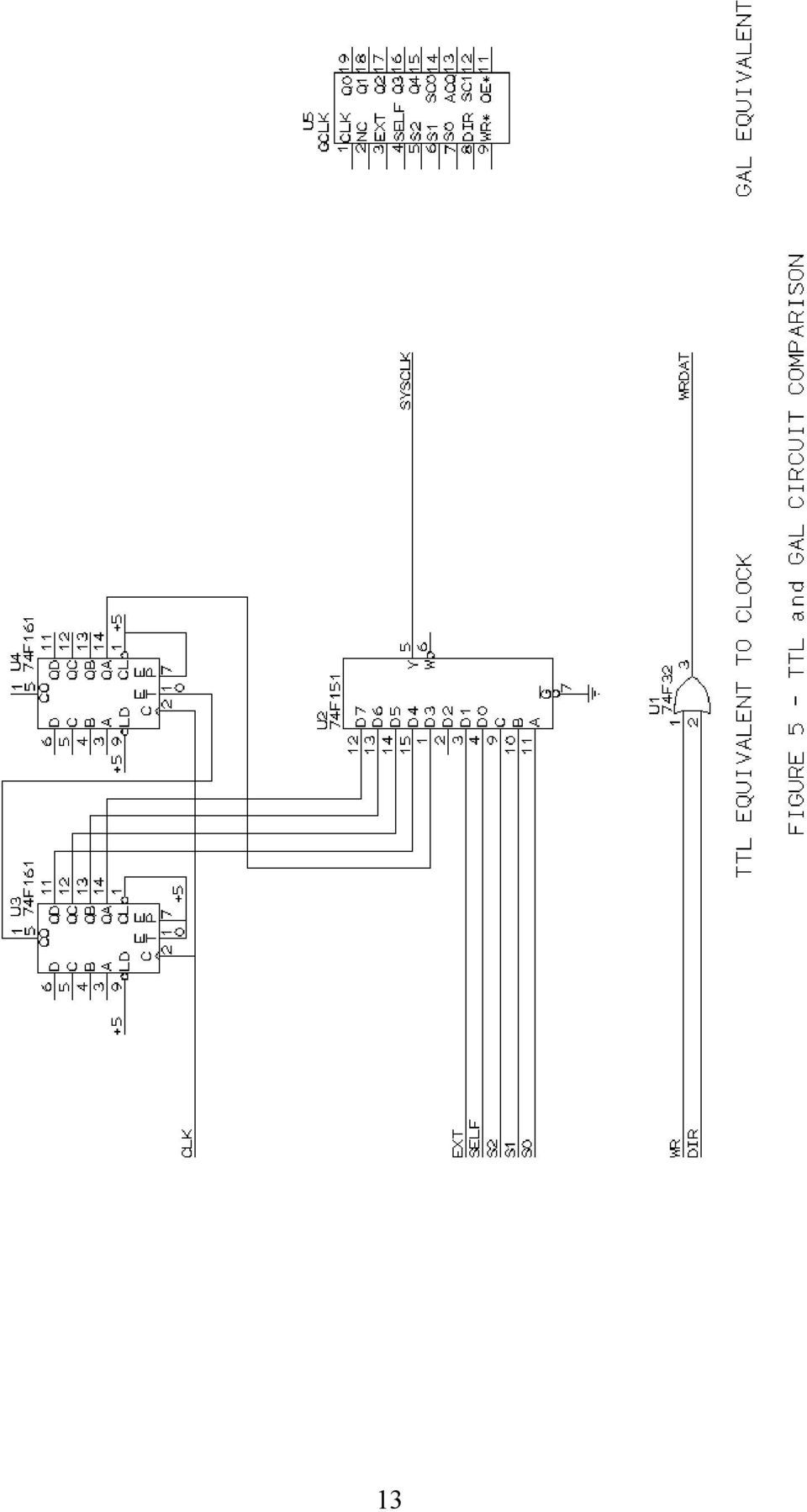
5 clk nc ext self s2 s1 s0 dir wr gnd /oe sysclk1 wrdat sysclk0 q4 q3 q2 q1 q0 vcc The symbolic names start with pin 1 and are assigned in order through pin 20. In this case pin 1 is assigned the name clk, pin 9 the name wr, pin 12 the name sysclk1 and pin 19 the name q0. If we later need to change the pin assignments, we simply rearranged the names given here. The equation section of the file is indicated by a line with the word EQUATIONS. Outputs q0, q1, q2, q3 and q4 form a 5 bit counter (a straight forward expansion of the 2 bit counter used before). This counter provides several reference frequencies at the outputs, q1 is half of q0, q2 is half of q1 etc. With a crystal oscillator of 40 Mhz connected to pin 1, q0 provides a 20 Mhz clock, q1 a 10 Mhz clock, q2 a 5 Mhz clock, q3 a 2.5 Mhz clock and q4 a 1.25 Mhz clock. The outputs sysclk0 and sysclk1 use identical equations, so I refer to them together as sysclk. The sysclk outputs are combinatorial, they allow the system clock to be selected from q0, q1, q2, q3, q4 or the inputs self or ext. The inputs s0, s1 and s2 select which clock is output to sysclk. From the equations you can see that if s0, s1 and s2 are all 0 then sysclk is the same as the input self. If s0, s1 and s2 are all 1 then the last product term will apply and sysclk will follow q0. The final output defined in the equations is wrdat, this is obviously just a simple two input OR function. I remember that Bill Kibler said he wanted to see the equivalent circuit in standard logic for all programmable logic used in TCJ. It is not always possible, but in this case I had first looked designing the logic analyzer using standard logic. The equivalent circuit to this GAL is shown in the schematic in figure 5, notice the savings in chip count and cost. The equation file is compiled it with the command line: EQN2JED -N CLOCK EQN2JED is the PLAN program that produces the JEDEC file, this will take our CLOCK.EQN file check it for errors and if error free produce the JEDEC file CLOCK.JED. The -n in the command line tells the program to produce a new log file, rather then append to the existing log file. The log file produced is CLOCK.LOG. The log file has a lot of interesting information about the programmed device the use of each device pin, the product term usage and the device pinout. A Memory Decoder Let's take a look at a real life example that was suggested to me by Dave Baldwin (Editor of The Computer Journal). Let's say that we are designing a Z80 based system and we would like the memory map to include an 8K EPROM at address 0000h, a 2K EEPROM at address 2000h and have the remainder of the 64K address space filled with static ram (2 32K devices). So a table of our memory map looks like: Address (hex) Device FFF EPROM FF EEPROM FFF SRAM FFFF SRAM1 5
.")
6 This type of decoding is a pain in the butt if we use standard TTL devices. We would need several devices and have to deal with the problems of propogation delays through the several levels of devices. If we use a 16V8 or 20V8 we can easily handle this decoding with one 20 or 24 pin device. Our total propogation delay will be the single propogation delay of the chip. This means we can have a propogation delay as low as 5 ns with a GAL rated at 5 ns. In addition we can include the decoding of the I/O space on the same chip. In this case defining the equations for each chip select output is very straight forward. We want the EPROM chip select to be active when address lines A15, A14 and A13 are low and the Z80 MREQ signal is low. Since the active state of the EPROM chip select is low we would express the equation as: /EPROM = /A15 * /A14 * /A13 * /MREQ The EEPROM chip select is only slightly more involved. The address range ff is selected when A15, A14, A12, A11 and MREQ are low, while A13 is high. This gives the equation: /EEPROM = /A15 * /A14 * A13 * /A12 * /A11 * /MREQ The first static ram has the most complicated equation (but still well within the capabilities of the 16V8). The FFF address space can be thought of as three regions FFF, FFF and FFF. The product terms defining each of these regions is then ORed together to define the complete equation as follows: /SRAM0 = /A15 * /A14 * A13 * /A12 * A11 * /MREQ + /A15 * /A14 * A13 * A12 * /MREQ + /A15 * A14 * /MREQ It is obvious that the equation for the second static RAM's chip select is: /SRAM1 = A15 * /MREQ The complete equation file with the I/O decoding using a 16V8 is printed above. If we wanted finer granularity on the I/O decode we could use a 20V8, this would give us 4 addition inputs for address lines, that could be included in the equations. If we wanted to have a 10 chip select outputs we could use a GAL22V10. Note that the pin out selected is arbitrary, in this case we could swap any of the input pins or any of the output pins just by redefining the pin list. This is a great aid if you do your own PC board design. I think this example shows you why I use programmable logic wherever I can. We have reduced our decode logic to one 20 pin device. In doing so we have reduced the number of interconnects, saved PC board space, saved money and saved both circuit and PC board design time. In addition we have increased our design flexibility and helped our parts inventory. If we later find that we must have a 16K EPROM instead of the 8K 6

7 EPROM. we can change our decode circuit by just reprogramming the GAL16V8. We can also replace our bin of spare TTL chips with few 16V8s. Once you start using programmable logic you can see the advantages continue to pile up. Circuit Layout When using PLDs you must use the same care in circuit layout as you would need to with any high speed logic device. Completely covering the topic of high speed circuit design would fill a book, but here are some things to look for. Be careful with the ground and power layouts to reduce the impedance of these signals to the chip. Use a decoupling capacitor as close as possible to each chip's power and ground pins. Device programmers The device programmer will program the device with logic as defined in the JEDEC file. One example of a device programmer that will program PLDs is the Alta Pro For more information check out the web site at I will also post follow on PLD design tutorial on the web site about using the 22V10. 7

8 ; GCLK.EQN Logic Analyzer U15 ; This is the declaration section CHIP GCLK 16V8 ; Pin labels here CLK NC EXT SELF S2 S1 S0 DIR WR GND OEN SC1 WRDAT SC0 Q4 Q3 Q2 Q1 Q0 VCC ; Next is the equation section EQUATIONS ; Q0 - Q4 form a 5 bit binary counter Q0 := /Q0 Q1 := Q0 * /Q1 + /Q0 * Q1 Q2 := Q0 * Q1 * /Q2 + Q2 * /Q0 + Q2 * /Q1 Q3 := Q0 * Q1 * Q2 * /Q3 + Q3 * /Q0 + Q3 * /Q1 + Q3 * /Q2 Q4 := Q0 * Q1 * Q2 * Q3 * /Q4 + Q4 * /Q0 + Q4 * /Q1 + Q4 * /Q2 + Q4 * /Q3 ; SC0 and SC1 output the system clock as selected by ; S0, S1 and S2 SC0 = /S0 * /S1 * /S2 * SELF + S0 * /S1 * /S2 * EXT + S0 * S1 * /S2 * Q4 + /S0 * /S1 * S2 * Q3 + S0 * /S1 * S2 * Q2 + /S0 * S1 * S2 * Q1 + S0 * S1 * S2 * Q0 SC1 = /S0 * /S1 * /S2 * SELF + S0 * /S1 * /S2 * EXT + S0 * S1 * /S2 * Q4 + /S0 * /S1 * S2 * Q3 + S0 * /S1 * S2 * Q2 + /S0 * S1 * S2 * Q1 + S0 * S1 * S2 * Q0 ; WRDAT is a simple OR function of WR and DIR WRDAT =WR + DIR 8

9 ; Z80 memory and I/O decoder example - TCJ ; Robert G. Brown - ALTA ENGINEERING (860) ; Memory Map ; FFF EPROM ; FF EEPROM ; FFF SRAM0 ; 8000-FFFF SRAM1 ; CHIP decode 16V8 ; set pinout - can be altered later if needed MREQ A15 A14 A13 A12 A11 IOREQ A7 A6 GND A5 EPROM EEPROM SRAM0 SRAM1 IO0 IO1 IO2 IO3 VCC EQUATIONS /EPROM = /A15 * /A14 * /A13 * /MREQ /EEPROM = /A15 * /A14 * A13 * /A12 * /A11 * /MREQ /SRAM0 = /A15 * /A14 * A13 * /A12 * A11 * /MREQ + /A15 * /A14 * A13 * A12 * /MREQ + /A15 * A14 * /MREQ /SRAM1 = A15 * /MREQ /IO0 = /A7 * /A6 * /A5 * /IOREQ /IO1 = /A7 * /A6 * A5 * /IOREQ /IO2 = /A7 * A6 * /A5 * /IOREQ /IO3 = /A7 * A6 * A5 * /IOREQ 9

10 10

11 11

12 12
13 13
Modeling Sequential Elements with Verilog. Prof. Chien-Nan Liu TEL: 03-4227151 ext:34534 Email: [email protected]. Sequential Circuit
 Modeling Sequential Elements with Verilog Prof. Chien-Nan Liu TEL: 03-4227151 ext:34534 Email: [email protected] 4-1 Sequential Circuit Outputs are functions of inputs and present states of storage elements
RAM & ROM Based Digital Design. ECE 152A Winter 2012
 RAM & ROM Based Digital Design ECE 152A Winter 212 Reading Assignment Brown and Vranesic 1 Digital System Design 1.1 Building Block Circuits 1.1.3 Static Random Access Memory (SRAM) 1.1.4 SRAM Blocks in
Lecture-3 MEMORY: Development of Memory:
 Lecture-3 MEMORY: It is a storage device. It stores program data and the results. There are two kind of memories; semiconductor memories & magnetic memories. Semiconductor memories are faster, smaller,
Having read this workbook you should be able to: recognise the arrangement of NAND gates used to form an S-R flip-flop.
 Objectives Having read this workbook you should be able to: recognise the arrangement of NAND gates used to form an S-R flip-flop. describe how such a flip-flop can be SET and RESET. describe the disadvantage
LAB #3 VHDL RECOGNITION AND GAL IC PROGRAMMING USING ALL-11 UNIVERSAL PROGRAMMER
 LAB #3 VHDL RECOGNITION AND GAL IC PROGRAMMING USING ALL-11 UNIVERSAL PROGRAMMER OBJECTIVES 1. Learn the basic elements of VHDL that are implemented in Warp. 2. Build a simple application using VHDL and
The components. E3: Digital electronics. Goals:
 E3: Digital electronics Goals: Basic understanding of logic circuits. Become familiar with the most common digital components and their use. Equipment: 1 st. LED bridge 1 st. 7-segment display. 2 st. IC
Module 2. Embedded Processors and Memory. Version 2 EE IIT, Kharagpur 1
 Module 2 Embedded Processors and Memory Version 2 EE IIT, Kharagpur 1 Lesson 5 Memory-I Version 2 EE IIT, Kharagpur 2 Instructional Objectives After going through this lesson the student would Pre-Requisite
NTE2053 Integrated Circuit 8 Bit MPU Compatible A/D Converter
 NTE2053 Integrated Circuit 8 Bit MPU Compatible A/D Converter Description: The NTE2053 is a CMOS 8 bit successive approximation Analog to Digital converter in a 20 Lead DIP type package which uses a differential
150127-Microprocessor & Assembly Language
 Chapter 3 Z80 Microprocessor Architecture The Z 80 is one of the most talented 8 bit microprocessors, and many microprocessor-based systems are designed around the Z80. The Z80 microprocessor needs an
CHAPTER 11: Flip Flops
 CHAPTER 11: Flip Flops In this chapter, you will be building the part of the circuit that controls the command sequencing. The required circuit must operate the counter and the memory chip. When the teach
A N. O N Output/Input-output connection
 Memory Types Two basic types: ROM: Read-only memory RAM: Read-Write memory Four commonly used memories: ROM Flash, EEPROM Static RAM (SRAM) Dynamic RAM (DRAM), SDRAM, RAMBUS, DDR RAM Generic pin configuration:
Latches, the D Flip-Flop & Counter Design. ECE 152A Winter 2012
 Latches, the D Flip-Flop & Counter Design ECE 52A Winter 22 Reading Assignment Brown and Vranesic 7 Flip-Flops, Registers, Counters and a Simple Processor 7. Basic Latch 7.2 Gated SR Latch 7.2. Gated SR
GAL-ASM-Starterkit. taskit GmbH Seelenbinderstr. 33 12555 Berlin (Germany) Telefon +49(0)30 / 611295-0 Fax +49(0)30 / 611295-10
 Telefon +49(0)30 / 611295-0 Fax +49(0)30 / 611295-10") GAL-ASM-Starterkit taskit GmbH Seelenbinderstr. 33 12555 Berlin (Germany) Telefon +49(0)30 / 611295-0 Fax +49(0)30 / 611295-10 Die Rechte der beiliegenden OPAL Jr.(tm) Software liegen bei der National
GAL-ASM-Starterkit taskit GmbH Seelenbinderstr. 33 12555 Berlin (Germany) Telefon +49(0)30 / 611295-0 Fax +49(0)30 / 611295-10 Die Rechte der beiliegenden OPAL Jr.(tm) Software liegen bei der National
DS1225Y 64k Nonvolatile SRAM
 DS1225Y 64k Nonvolatile SRAM www.maxim-ic.com FEATURES years minimum data retention in the absence of external power Data is automatically protected during power loss Directly replaces 2k x 8 volatile
Chapter 7 Memory and Programmable Logic
 NCNU_2013_DD_7_1 Chapter 7 Memory and Programmable Logic 71I 7.1 Introduction ti 7.2 Random Access Memory 7.3 Memory Decoding 7.5 Read Only Memory 7.6 Programmable Logic Array 77P 7.7 Programmable Array
Memory Basics. SRAM/DRAM Basics
 Memory Basics RAM: Random Access Memory historically defined as memory array with individual bit access refers to memory with both Read and Write capabilities ROM: Read Only Memory no capabilities for
Memory. The memory types currently in common usage are:
 ory ory is the third key component of a microprocessor-based system (besides the CPU and I/O devices). More specifically, the primary storage directly addressed by the CPU is referred to as main memory
Experiment # 9. Clock generator circuits & Counters. Eng. Waleed Y. Mousa
 Experiment # 9 Clock generator circuits & Counters Eng. Waleed Y. Mousa 1. Objectives: 1. Understanding the principles and construction of Clock generator. 2. To be familiar with clock pulse generation
Homework # 2. Solutions. 4.1 What are the differences among sequential access, direct access, and random access?
 ECE337 / CS341, Fall 2005 Introduction to Computer Architecture and Organization Instructor: Victor Manuel Murray Herrera Date assigned: 09/19/05, 05:00 PM Due back: 09/30/05, 8:00 AM Homework # 2 Solutions
To design digital counter circuits using JK-Flip-Flop. To implement counter using 74LS193 IC.
 8.1 Objectives To design digital counter circuits using JK-Flip-Flop. To implement counter using 74LS193 IC. 8.2 Introduction Circuits for counting events are frequently used in computers and other digital
DS1220Y 16k Nonvolatile SRAM
 Not Recommended for New Design DS122Y 16k Nonvolatile SRAM www.maxim-ic.com FEATURES years minimum data retention in the absence of external power Data is automatically protected during power loss Directly
ETEC 2301 Programmable Logic Devices. Chapter 10 Counters. Shawnee State University Department of Industrial and Engineering Technologies
 ETEC 2301 Programmable Logic Devices Chapter 10 Counters Shawnee State University Department of Industrial and Engineering Technologies Copyright 2007 by Janna B. Gallaher Asynchronous Counter Operation
Memory Elements. Combinational logic cannot remember
 Memory Elements Combinational logic cannot remember Output logic values are function of inputs only Feedback is needed to be able to remember a logic value Memory elements are needed in most digital logic
So far we have investigated combinational logic for which the output of the logic devices/circuits depends only on the present state of the inputs.
 equential Logic o far we have investigated combinational logic for which the output of the logic devices/circuits depends only on the present state of the inputs. In sequential logic the output of the
ECE410 Design Project Spring 2008 Design and Characterization of a CMOS 8-bit Microprocessor Data Path
 ECE410 Design Project Spring 2008 Design and Characterization of a CMOS 8-bit Microprocessor Data Path Project Summary This project involves the schematic and layout design of an 8-bit microprocessor data
Chapter 2 Logic Gates and Introduction to Computer Architecture
 Chapter 2 Logic Gates and Introduction to Computer Architecture 2.1 Introduction The basic components of an Integrated Circuit (IC) is logic gates which made of transistors, in digital system there are
BINARY CODED DECIMAL: B.C.D.
 BINARY CODED DECIMAL: B.C.D. ANOTHER METHOD TO REPRESENT DECIMAL NUMBERS USEFUL BECAUSE MANY DIGITAL DEVICES PROCESS + DISPLAY NUMBERS IN TENS IN BCD EACH NUMBER IS DEFINED BY A BINARY CODE OF 4 BITS.
Fairchild Solutions for 133MHz Buffered Memory Modules
 AN-5009 Fairchild Semiconductor Application Note April 1999 Revised December 2000 Fairchild Solutions for 133MHz Buffered Memory Modules Fairchild Semiconductor provides several products that are compatible
Contents COUNTER. Unit III- Counters
 COUNTER Contents COUNTER...1 Frequency Division...2 Divide-by-2 Counter... 3 Toggle Flip-Flop...3 Frequency Division using Toggle Flip-flops...5 Truth Table for a 3-bit Asynchronous Up Counter...6 Modulo
DS1220Y 16k Nonvolatile SRAM
 19-5579; Rev 10/10 NOT RECOENDED FOR NEW DESIGNS 16k Nonvolatile SRAM www.maxim-ic.com FEATURES 10 years minimum data retention in the absence of external power Data is automatically protected during power
Lecture 5: Gate Logic Logic Optimization
 Lecture 5: Gate Logic Logic Optimization MAH, AEN EE271 Lecture 5 1 Overview Reading McCluskey, Logic Design Principles- or any text in boolean algebra Introduction We could design at the level of irsim
Computer Systems Structure Main Memory Organization
 Computer Systems Structure Main Memory Organization Peripherals Computer Central Processing Unit Main Memory Computer Systems Interconnection Communication lines Input Output Ward 1 Ward 2 Storage/Memory
A Lesson on Digital Clocks, One Shots and Counters
 A Lesson on Digital Clocks, One Shots and Counters Topics Clocks & Oscillators LM 555 Timer IC Crystal Oscillators Selection of Variable Resistors Schmitt Gates Power-On Reset Circuits One Shots Counters
COMBINATIONAL and SEQUENTIAL LOGIC CIRCUITS Hardware implementation and software design
 PH-315 COMINATIONAL and SEUENTIAL LOGIC CIRCUITS Hardware implementation and software design A La Rosa I PURPOSE: To familiarize with combinational and sequential logic circuits Combinational circuits
A Lesson on Digital Clocks, One Shots and Counters
 A Lesson on Digital Clocks, One Shots and Counters Topics Clocks & Oscillators LM 555 Timer IC Crystal Oscillators Selection of Variable Resistors Schmitt Gates Power-On Reset Circuits One Shots Counters
Technical Note. Micron NAND Flash Controller via Xilinx Spartan -3 FPGA. Overview. TN-29-06: NAND Flash Controller on Spartan-3 Overview
 Technical Note TN-29-06: NAND Flash Controller on Spartan-3 Overview Micron NAND Flash Controller via Xilinx Spartan -3 FPGA Overview As mobile product capabilities continue to expand, so does the demand
Module 3: Floyd, Digital Fundamental
 Module 3: Lecturer : Yongsheng Gao Room : Tech - 3.25 Email : [email protected] Structure : 6 lectures 1 Tutorial Assessment: 1 Laboratory (5%) 1 Test (20%) Textbook : Floyd, Digital Fundamental
1. True or False? A voltage level in the range 0 to 2 volts is interpreted as a binary 1.
 File: chap04, Chapter 04 1. True or False? A voltage level in the range 0 to 2 volts is interpreted as a binary 1. 2. True or False? A gate is a device that accepts a single input signal and produces one
Computer Architecture
 Computer Architecture Random Access Memory Technologies 2015. április 2. Budapest Gábor Horváth associate professor BUTE Dept. Of Networked Systems and Services [email protected] 2 Storing data Possible
Modeling Latches and Flip-flops
 Lab Workbook Introduction Sequential circuits are digital circuits in which the output depends not only on the present input (like combinatorial circuits), but also on the past sequence of inputs. In effect,
Memory unit. 2 k words. n bits per word
 9- k address lines Read n data input lines Memory unit 2 k words n bits per word n data output lines 24 Pearson Education, Inc M Morris Mano & Charles R Kime 9-2 Memory address Binary Decimal Memory contents
PowerPC Microprocessor Clock Modes
 nc. Freescale Semiconductor AN1269 (Freescale Order Number) 1/96 Application Note PowerPC Microprocessor Clock Modes The PowerPC microprocessors offer customers numerous clocking options. An internal phase-lock
PLL frequency synthesizer
 ANALOG & TELECOMMUNICATION ELECTRONICS LABORATORY EXERCISE 4 Lab 4: PLL frequency synthesizer 1.1 Goal The goals of this lab exercise are: - Verify the behavior of a and of a complete PLL - Find capture
Lecture 8: Synchronous Digital Systems
 Lecture 8: Synchronous Digital Systems The distinguishing feature of a synchronous digital system is that the circuit only changes in response to a system clock. For example, consider the edge triggered
A New Paradigm for Synchronous State Machine Design in Verilog
 A New Paradigm for Synchronous State Machine Design in Verilog Randy Nuss Copyright 1999 Idea Consulting Introduction Synchronous State Machines are one of the most common building blocks in modern digital
Memory Systems. Static Random Access Memory (SRAM) Cell
 Cell") Memory Systems This chapter begins the discussion of memory systems from the implementation of a single bit. The architecture of memory chips is then constructed using arrays of bit implementations coupled
Memory Systems This chapter begins the discussion of memory systems from the implementation of a single bit. The architecture of memory chips is then constructed using arrays of bit implementations coupled
MACHINE ARCHITECTURE & LANGUAGE
 in the name of God the compassionate, the merciful notes on MACHINE ARCHITECTURE & LANGUAGE compiled by Jumong Chap. 9 Microprocessor Fundamentals A system designer should consider a microprocessor-based
MICROPROCESSOR AND MICROCOMPUTER BASICS
 Introduction MICROPROCESSOR AND MICROCOMPUTER BASICS At present there are many types and sizes of computers available. These computers are designed and constructed based on digital and Integrated Circuit
CS311 Lecture: Sequential Circuits
 CS311 Lecture: Sequential Circuits Last revised 8/15/2007 Objectives: 1. To introduce asynchronous and synchronous flip-flops (latches and pulsetriggered, plus asynchronous preset/clear) 2. To introduce
3.Basic Gate Combinations
 3.Basic Gate Combinations 3.1 TTL NAND Gate In logic circuits transistors play the role of switches. For those in the TTL gate the conducting state (on) occurs when the baseemmiter signal is high, and
Sequential Logic Design Principles.Latches and Flip-Flops
 Sequential Logic Design Principles.Latches and Flip-Flops Doru Todinca Department of Computers Politehnica University of Timisoara Outline Introduction Bistable Elements Latches and Flip-Flops S-R Latch
Chapter 9 Latches, Flip-Flops, and Timers
 ETEC 23 Programmable Logic Devices Chapter 9 Latches, Flip-Flops, and Timers Shawnee State University Department of Industrial and Engineering Technologies Copyright 27 by Janna B. Gallaher Latches A temporary
MM74HCT373 MM74HCT374 3-STATE Octal D-Type Latch 3-STATE Octal D-Type Flip-Flop
 3-STATE Octal D-Type Latch 3-STATE Octal D-Type Flip-Flop General Description The MM74HCT373 octal D-type latches and MM74HCT374 Octal D-type flip flops advanced silicongate CMOS technology, which provides
MICROPROCESSOR. Exclusive for IACE Students www.iace.co.in iacehyd.blogspot.in Ph: 9700077455/422 Page 1
 MICROPROCESSOR A microprocessor incorporates the functions of a computer s central processing unit (CPU) on a single Integrated (IC), or at most a few integrated circuit. It is a multipurpose, programmable
Introduction to Digital System Design
 Introduction to Digital System Design Chapter 1 1 Outline 1. Why Digital? 2. Device Technologies 3. System Representation 4. Abstraction 5. Development Tasks 6. Development Flow Chapter 1 2 1. Why Digital
Single 2.5V - 3.6V or 2.7V - 3.6V supply Atmel RapidS serial interface: 66MHz maximum clock frequency. SPI compatible modes 0 and 3
 32Mb, 2.5V or 2.7V Atmel ataflash ATASHEET Features Single 2.5V - 3.6V or 2.7V - 3.6V supply Atmel RapidS serial interface: 66MHz maximum clock frequency SPI compatible modes 0 and 3 User configurable
Master/Slave Flip Flops
 Master/Slave Flip Flops Page 1 A Master/Slave Flip Flop ( Type) Gated latch(master) Gated latch (slave) 1 Gate Gate GATE Either: The master is loading (the master in on) or The slave is loading (the slave
Read-only memory Implementing logic with ROM Programmable logic devices Implementing logic with PLDs Static hazards
 Points ddressed in this Lecture Lecture 8: ROM Programmable Logic Devices Professor Peter Cheung Department of EEE, Imperial College London Read-only memory Implementing logic with ROM Programmable logic
================================================================
 ==== ==== ================================================================ DR 6502 AER 201S Engineering Design 6502 Execution Simulator ================================================================
1-Mbit (128K x 8) Static RAM
 Static RAM") 1-Mbit (128K x 8) Static RAM Features Pin- and function-compatible with CY7C109B/CY7C1009B High speed t AA = 10 ns Low active power I CC = 80 ma @ 10 ns Low CMOS standby power I SB2 = 3 ma 2.0V Data Retention
1-Mbit (128K x 8) Static RAM Features Pin- and function-compatible with CY7C109B/CY7C1009B High speed t AA = 10 ns Low active power I CC = 80 ma @ 10 ns Low CMOS standby power I SB2 = 3 ma 2.0V Data Retention
INTEGRATED CIRCUITS. For a complete data sheet, please also download:
 INTEGRATED CIRCUITS DATA SEET For a complete data sheet, please also download: The IC6 74C/CT/CU/CMOS Logic Family Specifications The IC6 74C/CT/CU/CMOS Logic Package Information The IC6 74C/CT/CU/CMOS
ASYNCHRONOUS COUNTERS
 LB no.. SYNCHONOUS COUNTES. Introduction Counters are sequential logic circuits that counts the pulses applied at their clock input. They usually have 4 bits, delivering at the outputs the corresponding
DM9368 7-Segment Decoder/Driver/Latch with Constant Current Source Outputs
 DM9368 7-Segment Decoder/Driver/Latch with Constant Current Source Outputs General Description The DM9368 is a 7-segment decoder driver incorporating input latches and constant current output circuits
Decimal Number (base 10) Binary Number (base 2)
 Binary Number (base 2)") LECTURE 5. BINARY COUNTER Before starting with counters there is some vital information that needs to be understood. The most important is the fact that since the outputs of a digital chip can only be
LECTURE 5. BINARY COUNTER Before starting with counters there is some vital information that needs to be understood. The most important is the fact that since the outputs of a digital chip can only be
INTEGRATED CIRCUITS. For a complete data sheet, please also download:
 INTEGRATED CIRCUITS DATA SEET For a complete data sheet, please also download: The IC6 74C/CT/CU/CMOS ogic Family Specifications The IC6 74C/CT/CU/CMOS ogic Package Information The IC6 74C/CT/CU/CMOS ogic
TURBO PROGRAMMER USB, MMC, SIM DEVELOPMENT KIT
 TURBO PROGRAMMER USB, MMC, SIM DEVELOPMENT KIT HARDWARE GUIDE This document is part of Turbo Programmer documentation. For Developer Documentation, Applications and Examples, see http:/// PRELIMINARY (C)
Machine Architecture and Number Systems. Major Computer Components. Schematic Diagram of a Computer. The CPU. The Bus. Main Memory.
 1 Topics Machine Architecture and Number Systems Major Computer Components Bits, Bytes, and Words The Decimal Number System The Binary Number System Converting from Decimal to Binary Major Computer Components
SIMPLE EPROM PROGRAMMER. EPROM Programmer Design. Hardware
 Page 1 of 5 A simple EPROM programmer is described here. It connects to a PC's parallel port and can program EPROMs from 2716 to 27512. The design can be expanded to program even larger EPROMs. DOS based
Computers. Hardware. The Central Processing Unit (CPU) CMPT 125: Lecture 1: Understanding the Computer
 CMPT 125: Lecture 1: Understanding the Computer") Computers CMPT 125: Lecture 1: Understanding the Computer Tamara Smyth, [email protected] School of Computing Science, Simon Fraser University January 3, 2009 A computer performs 2 basic functions: 1.
Computers CMPT 125: Lecture 1: Understanding the Computer Tamara Smyth, [email protected] School of Computing Science, Simon Fraser University January 3, 2009 A computer performs 2 basic functions: 1.
Algorithms and Methods for Distributed Storage Networks 3. Solid State Disks Christian Schindelhauer
 Algorithms and Methods for Distributed Storage Networks 3. Solid State Disks Institut für Informatik Wintersemester 2007/08 Solid State Disks Motivation 2 10 5 1980 1985 1990 1995 2000 2005 2010 PRODUCTION
Flip-Flops and Sequential Circuit Design. ECE 152A Winter 2012
 Flip-Flops and Sequential Circuit Design ECE 52 Winter 22 Reading ssignment Brown and Vranesic 7 Flip-Flops, Registers, Counters and a Simple Processor 7.5 T Flip-Flop 7.5. Configurable Flip-Flops 7.6
Flip-Flops and Sequential Circuit Design
 Flip-Flops and Sequential Circuit Design ECE 52 Winter 22 Reading ssignment Brown and Vranesic 7 Flip-Flops, Registers, Counters and a Simple Processor 7.5 T Flip-Flop 7.5. Configurable Flip-Flops 7.6
8254 PROGRAMMABLE INTERVAL TIMER
 PROGRAMMABLE INTERVAL TIMER Y Y Y Compatible with All Intel and Most Other Microprocessors Handles Inputs from DC to 10 MHz 8 MHz 8254 10 MHz 8254-2 Status Read-Back Command Y Y Y Y Y Six Programmable
In-System Programming Design TM. Guidelines for ispjtag Devices. Introduction. Device-specific Connections. isplsi 1000EA Family.
 In-System Design TM February 2002 Introduction In-system programming (ISP ) has often been billed as a direct replacement for configuring a device through a programmer. The idea that devices can simply
AUTOMATIC NIGHT LAMP WITH MORNING ALARM USING MICROPROCESSOR
 AUTOMATIC NIGHT LAMP WITH MORNING ALARM USING MICROPROCESSOR INTRODUCTION This Project "Automatic Night Lamp with Morning Alarm" was developed using Microprocessor. It is the Heart of the system. The sensors
CHAPTER 3 Boolean Algebra and Digital Logic
 CHAPTER 3 Boolean Algebra and Digital Logic 3.1 Introduction 121 3.2 Boolean Algebra 122 3.2.1 Boolean Expressions 123 3.2.2 Boolean Identities 124 3.2.3 Simplification of Boolean Expressions 126 3.2.4
Programming Logic controllers
 Programming Logic controllers Programmable Logic Controller (PLC) is a microprocessor based system that uses programmable memory to store instructions and implement functions such as logic, sequencing,
The 104 Duke_ACC Machine
 The 104 Duke_ACC Machine The goal of the next two lessons is to design and simulate a simple accumulator-based processor. The specifications for this processor and some of the QuartusII design components
Programming PIC Microcontrollers in PicBasic Pro Lesson 1 Cornerstone Electronics Technology and Robotics II
 Programming PIC Microcontrollers in PicBasic Pro Lesson 1 Cornerstone Electronics Technology and Robotics II Administration: o Prayer PicBasic Pro Programs Used in This Lesson: o General PicBasic Pro Program
Digital Electronics Detailed Outline
 Digital Electronics Detailed Outline Unit 1: Fundamentals of Analog and Digital Electronics (32 Total Days) Lesson 1.1: Foundations and the Board Game Counter (9 days) 1. Safety is an important concept
Sequential Logic. (Materials taken from: Principles of Computer Hardware by Alan Clements )
") Sequential Logic (Materials taken from: Principles of Computer Hardware by Alan Clements ) Sequential vs. Combinational Circuits Combinatorial circuits: their outputs are computed entirely from their present
Sequential Logic (Materials taken from: Principles of Computer Hardware by Alan Clements ) Sequential vs. Combinational Circuits Combinatorial circuits: their outputs are computed entirely from their present
Lesson 12 Sequential Circuits: Flip-Flops
 Lesson 12 Sequential Circuits: Flip-Flops 1. Overview of a Synchronous Sequential Circuit We saw from last lesson that the level sensitive latches could cause instability in a sequential system. This instability
BP-2600 Concurrent Programming System
 BP-2600 Concurrent Programming System! With BP s 6th Generation Technology, the BP-2600 is the fastest universal production programmer available! Very Low Voltage Support down to 1.5V! Concurrent Programming
DDR4 Memory Technology on HP Z Workstations
 Technical white paper DDR4 Memory Technology on HP Z Workstations DDR4 is the latest memory technology available for main memory on mobile, desktops, workstations, and server computers. DDR stands for
Lab 11 Digital Dice. Figure 11.0. Digital Dice Circuit on NI ELVIS II Workstation
 Lab 11 Digital Dice Figure 11.0. Digital Dice Circuit on NI ELVIS II Workstation From the beginning of time, dice have been used for games of chance. Cubic dice similar to modern dice date back to before
We r e going to play Final (exam) Jeopardy! "Answers:" "Questions:" - 1 -
 Jeopardy! Answers: Questions: - 1 -") . (0 pts) We re going to play Final (exam) Jeopardy! Associate the following answers with the appropriate question. (You are given the "answers": Pick the "question" that goes best with each "answer".)
. (0 pts) We re going to play Final (exam) Jeopardy! Associate the following answers with the appropriate question. (You are given the "answers": Pick the "question" that goes best with each "answer".)
A Verilog HDL Test Bench Primer Application Note
 A Verilog HDL Test Bench Primer Application Note Table of Contents Introduction...1 Overview...1 The Device Under Test (D.U.T.)...1 The Test Bench...1 Instantiations...2 Figure 1- DUT Instantiation...2
W25Q80, W25Q16, W25Q32 8M-BIT, 16M-BIT AND 32M-BIT SERIAL FLASH MEMORY WITH DUAL AND QUAD SPI
 8M-BIT, 16M-BIT AND 32M-BIT SERIAL FLASH MEMORY WITH DUAL AND QUAD SPI - 1 - Preliminary - Revision B Table of Contents 1. GENERAL DESCRIPTION... 5 2. FEATURES... 5 3. PIN CONFIGURATION SOIC 208-MIL...
Lecture N -1- PHYS 3330. Microcontrollers
 Lecture N -1- PHYS 3330 Microcontrollers If you need more than a handful of logic gates to accomplish the task at hand, you likely should use a microcontroller instead of discrete logic gates 1. Microcontrollers
Digital Systems Based on Principles and Applications of Electrical Engineering/Rizzoni (McGraw Hill
 Digital Systems Based on Principles and Applications of Electrical Engineering/Rizzoni (McGraw Hill Objectives: Analyze the operation of sequential logic circuits. Understand the operation of digital counters.
www.jameco.com 1-800-831-4242
 Distributed by: www.jameco.com 1-800-831-4242 The content and copyrights of the attached material are the property of its owner. www.maxim-ic.com FEATURES 10 years minimum data retention in the absence
Interfacing Analog to Digital Data Converters
 Converters In most of the cases, the PIO 8255 is used for interfacing the analog to digital converters with microprocessor. We have already studied 8255 interfacing with 8086 as an I/O port, in previous
SECTION C [short essay] [Not to exceed 120 words, Answer any SIX questions. Each question carries FOUR marks] 6 x 4=24 marks
![SECTION C [short essay] [Not to exceed 120 words, Answer any SIX questions. Each question carries FOUR marks] 6 x 4=24 marks](/thumbs/35/17285180.jpg "SECTION C [short essay] [Not to exceed 120 words, Answer any SIX questions. Each question carries FOUR marks] 6 x 4=24 marks") UNIVERSITY OF KERALA First Degree Programme in Computer Applications Model Question Paper Semester I Course Code- CP 1121 Introduction to Computer Science TIME : 3 hrs Maximum Mark: 80 SECTION A [Very
UNIVERSITY OF KERALA First Degree Programme in Computer Applications Model Question Paper Semester I Course Code- CP 1121 Introduction to Computer Science TIME : 3 hrs Maximum Mark: 80 SECTION A [Very
PART B QUESTIONS AND ANSWERS UNIT I
 PART B QUESTIONS AND ANSWERS UNIT I 1. Explain the architecture of 8085 microprocessor? Logic pin out of 8085 microprocessor Address bus: unidirectional bus, used as high order bus Data bus: bi-directional
8-Bit Flash Microcontroller for Smart Cards. AT89SCXXXXA Summary. Features. Description. Complete datasheet available under NDA
 Features Compatible with MCS-51 products On-chip Flash Program Memory Endurance: 1,000 Write/Erase Cycles On-chip EEPROM Data Memory Endurance: 100,000 Write/Erase Cycles 512 x 8-bit RAM ISO 7816 I/O Port
White Paper Utilizing Leveling Techniques in DDR3 SDRAM Memory Interfaces
 White Paper Introduction The DDR3 SDRAM memory architectures support higher bandwidths with bus rates of 600 Mbps to 1.6 Gbps (300 to 800 MHz), 1.5V operation for lower power, and higher densities of 2
DIGITAL TECHNICS II. Dr. Bálint Pődör. Óbuda University, Microelectronics and Technology Institute
 DIGITAL TECHNICS II Dr. Bálint Pődör Óbuda University, Microelectronics and Technology Institute 2. LECTURE: ELEMENTARY SEUENTIAL CIRCUITS: FLIP-FLOPS 1st year BSc course 2nd (Spring) term 2012/2013 1
Feature EPM5032 EPM5064 EPM5128 EPM5130 EPM5192
 MAX 5000 Programmable Logic Device Family May 1999, ver. 5 Data Sheet Features... Advanced Multiple Array MatriX (MAX ) 5000 architecture combining speed and ease-of-use of PAL devices with the density
PROGETTO DI SISTEMI ELETTRONICI DIGITALI. Digital Systems Design. Digital Circuits Advanced Topics
 PROGETTO DI SISTEMI ELETTRONICI DIGITALI Digital Systems Design Digital Circuits Advanced Topics 1 Sequential circuit and metastability 2 Sequential circuit - FSM A Sequential circuit contains: Storage