Common Base BJT Amplifier Common Collector BJT Amplifier
|
|
|
- Emmeline West
- 9 years ago
- Views:
Transcription
1 Common Base BJT Amplifier Common Collector BJT Amplifier Common Collector (Emitter Follower) Configuration Common Base Configuration Small Signal Analysis Design Example Amplifier Input and Output Impedances 1

2 Basic Single BJT Amplifier Features CE Amplifier CC Amplifier CB Amplifier Voltage Gain (A V ) moderate (-R C /R E ) low (about 1) high Current Gain (A I ) moderate ( ) moderate ( 1) low (about 1) Input Resistance high high low Output Resistance high low high CE BJT amplifier => CS MOS amplifier CC BJT amplifier => CD MOS amplifier CB BJT amplifier => CG MOS amplifier 2

3 Common Collector ( Emitter Follower) Amplifier In the emitter follower, the output voltage is taken between emitter and ground. The voltage gain of this amplifier is nearly one the output follows the input - hence the name: emitter follower. 3

4 Emitter Follower Biasing i B Vb i E i C Then, choose/specified I E, and the rest of the design follows: R E = V E I E = V CC/2 0.7 I E Split bias voltage drops about equally across the transistor V CE (or V CB ) and V Re (or V B ). For simplicity,choose: V B = V CC 2 R 1 =R 2 For an assumed = 100: As with CE bias design, stable op. pt. => R B 1 R E, i.e. R B =R 1 R 2 = R 1 2 = 1 R E R E R 1 =R 2 =20 R E 4

5 Typical Design Choose: I E =1mA V CC =12V And the rest of the design follows immediately: R E = V E I E = 12/ =5.3k Use standard sizes! R E =5.1k R 1 =R 2 =100 k i B Vb i E i C 5

6 Equivalent Circuits R B =R 1 R 2 <=> Rb V CC /2 6

7 Multisim Bias Check I E V Rb =I B R B = 1 R B=0.495V i B <=> VRb - + Rb Identical results as expected! 7

8 Emitter Follower Small Signal Circuit Mid-band equivalent circuit: v sig ' = R B v R B R sig = 50 S v v sig sig R TH =R S R B = R S R S Rb Small signal mid-band circuit - where C B has negligible reactance (above ). Thevenin circuit consisting of R and R shows min S B effect of R B negligible, since it is much larger than R S. 8
.")
9 Follower Small Signal Analysis - Voltage Gain Circuit analysis: v sig = R S r 1 R E i b i b Solving for i b i e i b = v sig R S r 1 R E v out = R E 1 v sig R S r 1 R E A V = v out v sig = R E v sig 1 R S r 1 R E 9

10 Small Signal Analysis Voltage Gain - cont. v out v sig = R E R S r 1 R E Since, typically: R S r 1 R E A V = v out R E =1 v sig R E Note: A V is non-inverting 10

11 Blocking Capacitor - C B - Selection + i b Use the base current expression: vbg Rb - v bg =r i b R E i E = r 1 i b i b = v bg r 1 R E R B =50 k R S R S =50 R in r bg = v bg i b =r 1 R E 1 R E = k=515k To obtain the base to ground resistance of the transistor: This transistor input resistance is in parallel with the 50 k R B, forming the total amplifier input resistance: R i n =R S R B r bg R B r bg = k =45.6 k

12 C B Selection cont. Choose C B such that its reactance is 1/10 of R in at : min 1 = R i n C B 10 C B 10 min R i n C B F Assume the lowest frequency is 20 Hz: min = = =100 R i n 46 k Pick C B = 2 F (two 1 F caps in parallel), the nearest standard value in the RCA Lab. We could be (unnecessarily) more precise and include R s as part of the total resistance in the loop. It is very small compared to R in. 12
, the nearest standard value in the RCA Lab.")
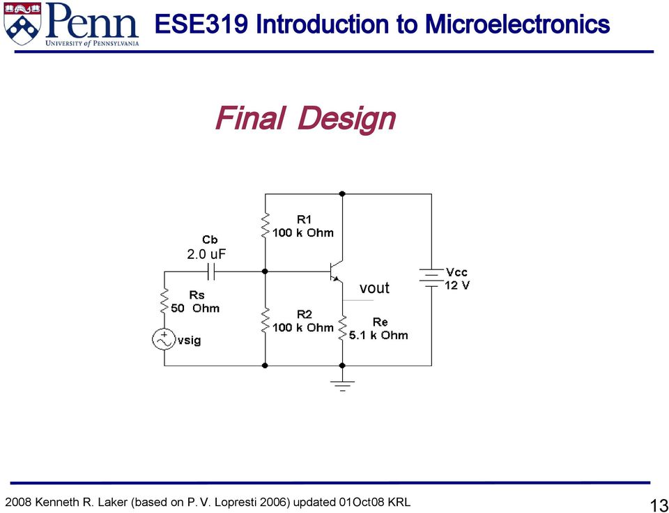
13 Final Design 2.0 uf 13

14 Multisim Simulation Results 20 Hz. Data 1 Khz. Data 14

15 Of What value is a Unity Gain Amplifier? i b i e To answer this question, we must examine the output impedance of the amplifier and its power gain. 15

16 Emitter Follower Output Resistance i b 0 i x R B =50 k R S Assume: v x R out I C =1 ma r = V T = V T =2500 I B I C =100 R S =50 i x = i b i b = 1 i b i b = i x 1 v x = i b Rs r = R S r 1 i x R out = v x = R S r i x 1 r 1 R out is the Thevenin resistance looking into the open-circuit output. R out =

17 Multisim Verification of R out Rin Rout Thevenin equivalent for the short-circuited emitter follower. If was 200, as for most good NPN transistors, R out would be lower - close to 12. i sc =i x Av*vsig A V = 1 <=> + R in =R S r 1 R E R L 1 R L v oc =A V v sig - i sc =i x Multisim short circuit check ( = 100, v out = v sig ): i x = 1 i x v sig = R S i b r i b R out = A V v sig = R r S i x 1 R out = v oc i sc = A V v sig rms i sc rms = =
: i x = 1 i x v sig = R S i b r i b R out = A V v sig = R r S i x 1 R out = v oc i")
18 Equivalent Circuits with Load R L i b i e RL Z in = v sig i e ' <=> Rin + - Rout Av*vsig + vload - RL Re R in =R S r 1 R E R L 1 R L R out = v sig rms i sc rms = =

19 Emitter Follower Power Gain Consider the case where a R L = 50 load is connected through an infinite capacitor to the emitter of the follower we designed. Using its Thevenin equivalent: vsig isig Rin v load = R L A V v sig R L R out = v sig= 2 3 v sig i load = A V v sig = v sig R out R L 75 p load =v load i load = v 2 sig + - Rout 25 iload Av*vsig vth=g vsig C= + vload - R L load is in parallel with 5.1k R E and dominates: i sig =i b = v sig R in A V 1 v sig 1 R E R L p sig =v sig i sig v 2 sig v sig G pwr = p load = = p sig

20 The Common Base Amplifier Voltage Bias Design Current Bias Design 20

21 Common Base Configuration Both voltage and current biasing follow the same rules as those applied to the common emitter amplifier. As before, insert a blocking capacitor in the input signal path to avoid disturbing the dc bias. The common base amplifier uses a bypass capacitor or a direct connection from base to ground to hold the base at ground for the signal only! The common emitter amplifier (except for intentional R E feedback) holds the emitter at signal ground, while the common collector circuit does the same for the collector. 21
22 Voltage Bias Common Base Design 47k Ohm 4.7 k Ohm 5.1k Ohm 470 Ohm We keep the same bias that we established for the gain of 10 common emitter amplifier. All that we need to do is pick the capacitor values and calculate the circuit gain. 22
23 i' b Common Base Small Signal Analysis - C i b i' e i e 4.7 k Ohm i c I' c Determine C IN : (let C B = ) IN Find a equivalent impedance for the input circuit, R S, C IN, and R E2 : i sig 470 Ohm v Re2 = R E2 r e R E2 r e R S 1 j C IN v sig r e = r 1 Z in r e R E2 r e ideally v Re2 = v for R min E2 r e R sig S 1 R min C S R E2 r e 1 = R S r e 10 C IN min C IN 10 IN = min R S r e 23
24 Determine C IN cont. A suitable value for C IN for a 20 Hz lower frequency: 10 min C IN R S r e 1 C IN 2 min R S r e = F or C IN = F! Not too practical! Must choose smaller value of C IN. 1. Choose: min C IN R S r e =1 2. Choose larger min 24
25 i b i' b R E2 >> R S i' e Small-signal Analysis - C i' c ib' i c B Determine C B : (let C IN = ) Note the reference current reversals (due to v sig polarity)! v sig =R S i ' r 1 e j C B v sig =R S i ' r e 1 j C B i ' b i e i e ' 1 Determine Z in Z in = v sig i e ' i e ' = 1 1 R S r 1 j C B v sig 25
26 Determine C B i' b i' c ib' i e ' = 1 1 R S r 1 j C B v sig i' e i e ' = v sig R E2 >> R S R S 1 1 r 1 j C B Z in Z in = v sig i e ' =R S 1 1 r 1 j C B ideally Z in R S r 1 1 C B 1 R S r for min 26
27 Determine - C B cont. i' b i' c ib' For min Z in R S r 1 1 C B 1 R S r R E2 >> R S i' e Choose: C B 10 min 1 R S r F i.e. 10 C B =10.5 F 27
28 Small-signal Analysis Voltage Gain R E2 >> R S ib' i e ' 1 R S r 1 v sig = 1 R S r e v sig ' v out =R C i c = R C i ' e = 1 R C R S r e v sig Assume: C B =C IN = A V = v out = R C = 100 v sig 1 R S r e
29 Multisim Simulation 1062 uf 29

30 Multisim Frequency Response 20 Hz. response 1 KHZ. Response 30
Common Emitter BJT Amplifier Design Current Mirror Design
 Common Emitter BJT Amplifier Design Current Mirror Design 1 Some Random Observations Conditions for stabilized voltage source biasing Emitter resistance, R E, is needed. Base voltage source will have finite
Bipolar Junction Transistors
 Bipolar Junction Transistors Physical Structure & Symbols NPN Emitter (E) n-type Emitter region p-type Base region n-type Collector region Collector (C) B C Emitter-base junction (EBJ) Base (B) (a) Collector-base
Common-Emitter Amplifier
 Common-Emitter Amplifier A. Before We Start As the title of this lab says, this lab is about designing a Common-Emitter Amplifier, and this in this stage of the lab course is premature, in my opinion,
Physics 623 Transistor Characteristics and Single Transistor Amplifier Sept. 13, 2006
 Physics 623 Transistor Characteristics and Single Transistor Amplifier Sept. 13, 2006 1 Purpose To measure and understand the common emitter transistor characteristic curves. To use the base current gain
LABORATORY 2 THE DIFFERENTIAL AMPLIFIER
 LABORATORY 2 THE DIFFERENTIAL AMPLIFIER OBJECTIVES 1. To understand how to amplify weak (small) signals in the presence of noise. 1. To understand how a differential amplifier rejects noise and common
Transistor Characteristics and Single Transistor Amplifier Sept. 8, 1997
 Physics 623 Transistor Characteristics and Single Transistor Amplifier Sept. 8, 1997 1 Purpose To measure and understand the common emitter transistor characteristic curves. To use the base current gain
CHAPTER 10 OPERATIONAL-AMPLIFIER CIRCUITS
 CHAPTER 10 OPERATIONAL-AMPLIFIER CIRCUITS Chapter Outline 10.1 The Two-Stage CMOS Op Amp 10.2 The Folded-Cascode CMOS Op Amp 10.3 The 741 Op-Amp Circuit 10.4 DC Analysis of the 741 10.5 Small-Signal Analysis
BJT AC Analysis 1 of 38. The r e Transistor model. Remind Q-poiint re = 26mv/IE
 BJT AC Analysis 1 of 38 The r e Transistor model Remind Q-poiint re = 26mv/IE BJT AC Analysis 2 of 38 Three amplifier configurations, Common Emitter Common Collector (Emitter Follower) Common Base BJT
Voltage Divider Bias
 Voltage Divider Bias ENGI 242 ELEC 222 BJT Biasing 3 For the Voltage Divider Bias Configurations Draw Equivalent Input circuit Draw Equivalent Output circuit Write necessary KVL and KCL Equations Determine
The 2N3393 Bipolar Junction Transistor
 The 2N3393 Bipolar Junction Transistor Common-Emitter Amplifier Aaron Prust Abstract The bipolar junction transistor (BJT) is a non-linear electronic device which can be used for amplification and switching.
The basic cascode amplifier consists of an input common-emitter (CE) configuration driving an output common-base (CB), as shown above.
 configuration driving an output common-base (CB), as shown above.") Cascode Amplifiers by Dennis L. Feucht Two-transistor combinations, such as the Darlington configuration, provide advantages over single-transistor amplifier stages. Another two-transistor combination
Cascode Amplifiers by Dennis L. Feucht Two-transistor combinations, such as the Darlington configuration, provide advantages over single-transistor amplifier stages. Another two-transistor combination
The BJT Differential Amplifier. Basic Circuit. DC Solution
 c Copyright 010. W. Marshall Leach, Jr., Professor, Georgia Institute of Technology, School of Electrical and Computer Engineering. The BJT Differential Amplifier Basic Circuit Figure 1 shows the circuit
TWO PORT NETWORKS h-parameter BJT MODEL
 TWO PORT NETWORKS h-parameter BJT MODEL The circuit of the basic two port network is shown on the right. Depending on the application, it may be used in a number of different ways to develop different
Transistor Amplifiers
 Physics 3330 Experiment #7 Fall 1999 Transistor Amplifiers Purpose The aim of this experiment is to develop a bipolar transistor amplifier with a voltage gain of minus 25. The amplifier must accept input
ENEE 307 Electronic Circuit Design Laboratory Spring 2012. A. Iliadis Electrical Engineering Department University of Maryland College Park MD 20742
 1.1. Differential Amplifiers ENEE 307 Electronic Circuit Design Laboratory Spring 2012 A. Iliadis Electrical Engineering Department University of Maryland College Park MD 20742 Differential Amplifiers
Bipolar Transistor Amplifiers
 Physics 3330 Experiment #7 Fall 2005 Bipolar Transistor Amplifiers Purpose The aim of this experiment is to construct a bipolar transistor amplifier with a voltage gain of minus 25. The amplifier must
MAS.836 HOW TO BIAS AN OP-AMP
 MAS.836 HOW TO BIAS AN OP-AMP Op-Amp Circuits: Bias, in an electronic circuit, describes the steady state operating characteristics with no signal being applied. In an op-amp circuit, the operating characteristic
BJT Characteristics and Amplifiers
 BJT Characteristics and Amplifiers Matthew Beckler [email protected] EE2002 Lab Section 003 April 2, 2006 Abstract As a basic component in amplifier design, the properties of the Bipolar Junction Transistor
LAB VII. BIPOLAR JUNCTION TRANSISTOR CHARACTERISTICS
 LAB VII. BIPOLAR JUNCTION TRANSISTOR CHARACTERISTICS 1. OBJECTIVE In this lab, you will study the DC characteristics of a Bipolar Junction Transistor (BJT). 2. OVERVIEW You need to first identify the physical
Unit/Standard Number. High School Graduation Years 2010, 2011 and 2012
 1 Secondary Task List 100 SAFETY 101 Demonstrate an understanding of State and School safety regulations. 102 Practice safety techniques for electronics work. 103 Demonstrate an understanding of proper
BJT Circuit Configurations
 BJT Circuit Configurations V be ~ ~ ~ v s R L v s R L V Vcc R s cc R s v s R s R L V cc Common base Common emitter Common collector Common emitter current gain BJT Current-Voltage Characteristics V CE,
BJT AC Analysis. by Kenneth A. Kuhn Oct. 20, 2001, rev Aug. 31, 2008
 by Kenneth A. Kuhn Oct. 20, 2001, rev Aug. 31, 2008 Introduction This note will discuss AC analysis using the beta, re transistor model shown in Figure 1 for the three types of amplifiers: common-emitter,
BJT Amplifier Circuits
 JT Amplifier ircuits As we have developed different models for D signals (simple large-signal model) and A signals (small-signal model), analysis of JT circuits follows these steps: D biasing analysis:
BJT Amplifier Circuits
 JT Amplifier ircuits As we have developed different models for D signals (simple large-signal model) and A signals (small-signal model), analysis of JT circuits follows these steps: D biasing analysis:
Chapter 8 Differential and Multistage Amplifiers. EE 3120 Microelectronics II
 1 Chapter 8 Differential and Multistage Amplifiers Operational Amplifier Circuit Components 2 1. Ch 7: Current Mirrors and Biasing 2. Ch 9: Frequency Response 3. Ch 8: Active-Loaded Differential Pair 4.
Differential Amplifier Common & Differential Modes
 Differential Amplifier Common & Differential Modes Common & Differential Modes BJT Differential Amplifier Diff. Amp Voltage Gain and Input Impedance Small Signal Analysis Differential Mode Small Signal
Figure 1: Common-base amplifier.
 The Common-Base Amplifier Basic Circuit Fig. 1 shows the circuit diagram of a single stage common-base amplifier. The object is to solve for the small-signal voltage gain, input resistance, and output
Transistor Biasing. The basic function of transistor is to do amplification. Principles of Electronics
 192 9 Principles of Electronics Transistor Biasing 91 Faithful Amplification 92 Transistor Biasing 93 Inherent Variations of Transistor Parameters 94 Stabilisation 95 Essentials of a Transistor Biasing
Programmable Single-/Dual-/Triple- Tone Gong SAE 800
 Programmable Single-/Dual-/Triple- Tone Gong Preliminary Data SAE 800 Bipolar IC Features Supply voltage range 2.8 V to 18 V Few external components (no electrolytic capacitor) 1 tone, 2 tones, 3 tones
Differential Amplifier Offset. Causes of dc voltage and current offset Modeling dc offset R C
 ESE39 ntroduction to Microelectronics Differential Amplifier Offset Causes of dc voltage and current offset Modeling dc offset mismatch S mismatch β mismatch transistor mismatch dc offsets in differential
Amplifier Teaching Aid
 Amplifier Teaching Aid Table of Contents Amplifier Teaching Aid...1 Preface...1 Introduction...1 Lesson 1 Semiconductor Review...2 Lesson Plan...2 Worksheet No. 1...7 Experiment No. 1...7 Lesson 2 Bipolar
Chapter 12: The Operational Amplifier
 Chapter 12: The Operational Amplifier 12.1: Introduction to Operational Amplifier (Op-Amp) Operational amplifiers (op-amps) are very high gain dc coupled amplifiers with differential inputs; they are used
11: AUDIO AMPLIFIER I. INTRODUCTION
 11: AUDIO AMPLIFIER I. INTRODUCTION The properties of an amplifying circuit using an op-amp depend primarily on the characteristics of the feedback network rather than on those of the op-amp itself. A
OPERATIONAL AMPLIFIERS
 INTRODUCTION OPERATIONAL AMPLIFIERS The student will be introduced to the application and analysis of operational amplifiers in this laboratory experiment. The student will apply circuit analysis techniques
Electronics. Discrete assembly of an operational amplifier as a transistor circuit. LD Physics Leaflets P4.2.1.1
 Electronics Operational Amplifier Internal design of an operational amplifier LD Physics Leaflets Discrete assembly of an operational amplifier as a transistor circuit P4.2.1.1 Objects of the experiment
LAB VIII. BIPOLAR JUNCTION TRANSISTOR CHARACTERISTICS
 LAB VIII. BIPOLAR JUNCTION TRANSISTOR CHARACTERISTICS 1. OBJECTIVE In this lab, you will study the DC characteristics of a Bipolar Junction Transistor (BJT). 2. OVERVIEW In this lab, you will inspect the
Analog Signal Conditioning
 Analog Signal Conditioning Analog and Digital Electronics Electronics Digital Electronics Analog Electronics 2 Analog Electronics Analog Electronics Operational Amplifiers Transistors TRIAC 741 LF351 TL084
6.101 Final Project Report Class G Audio Amplifier
 6.101 Final Project Report Class G Audio Amplifier Mark Spatz 4/3/2014 1 1 Introduction For my final project, I designed and built a 150 Watt audio amplifier to replace the underpowered and unreliable
Transistors. NPN Bipolar Junction Transistor
 Transistors They are unidirectional current carrying devices with capability to control the current flowing through them The switch current can be controlled by either current or voltage ipolar Junction
Lecture 060 Push-Pull Output Stages (1/11/04) Page 060-1. ECE 6412 - Analog Integrated Circuits and Systems II P.E. Allen - 2002
 Page 060-1. ECE 6412 - Analog Integrated Circuits and Systems II P.E. Allen - 2002") Lecture 060 PushPull Output Stages (1/11/04) Page 0601 LECTURE 060 PUSHPULL OUTPUT STAGES (READING: GHLM 362384, AH 226229) Objective The objective of this presentation is: Show how to design stages that
Lecture 060 PushPull Output Stages (1/11/04) Page 0601 LECTURE 060 PUSHPULL OUTPUT STAGES (READING: GHLM 362384, AH 226229) Objective The objective of this presentation is: Show how to design stages that
Lab 7: Operational Amplifiers Part I
 Lab 7: Operational Amplifiers Part I Objectives The objective of this lab is to study operational amplifier (op amp) and its applications. We will be simulating and building some basic op amp circuits,
http://users.ece.gatech.edu/~mleach/ece3050/notes/feedback/fbexamples.pdf
 c Copyright 2009. W. Marshall Leach, Jr., Professor, Georgia Institute of Technology, School of Electrical and Computer Engineering. Feedback Amplifiers CollectionofSolvedProblems A collection of solved
Lecture 23: Common Emitter Amplifier Frequency Response. Miller s Theorem.
 Whites, EE 320 ecture 23 Page 1 of 17 ecture 23: Common Emitter mplifier Frequency Response. Miller s Theorem. We ll use the high frequency model for the BJT we developed the previous lecture and compute
Objectives The purpose of this lab is build and analyze Differential amplifiers based on NPN transistors (or NMOS transistors).
.") 1 Lab 03: Differential Amplifiers (BJT) (20 points) NOTE: 1) Please use the basic current mirror from Lab01 for the second part of the lab (Fig. 3). 2) You can use the same chip as the basic current mirror;
1 Lab 03: Differential Amplifiers (BJT) (20 points) NOTE: 1) Please use the basic current mirror from Lab01 for the second part of the lab (Fig. 3). 2) You can use the same chip as the basic current mirror;
Laboratory 4: Feedback and Compensation
 Laboratory 4: Feedback and Compensation To be performed during Week 9 (Oct. 20-24) and Week 10 (Oct. 27-31) Due Week 11 (Nov. 3-7) 1 Pre-Lab This Pre-Lab should be completed before attending your regular
Collection of Solved Feedback Amplifier Problems
 c Copyright 2009. W. Marshall Leach, Jr., Professor, Georgia Institute of Technology, School of Electrical and Computer Engineering. Collection of Solved Feedback Amplifier Problems This document contains
3.4 - BJT DIFFERENTIAL AMPLIFIERS
 BJT Differential Amplifiers (6/4/00) Page 1 3.4 BJT DIFFERENTIAL AMPLIFIERS INTRODUCTION Objective The objective of this presentation is: 1.) Define and characterize the differential amplifier.) Show the
Section 3. Sensor to ADC Design Example
 Section 3 Sensor to ADC Design Example 3-1 This section describes the design of a sensor to ADC system. The sensor measures temperature, and the measurement is interfaced into an ADC selected by the systems
Basic Electronics Prof. Dr. Chitralekha Mahanta Department of Electronics and Communication Engineering Indian Institute of Technology, Guwahati
 Basic Electronics Prof. Dr. Chitralekha Mahanta Department of Electronics and Communication Engineering Indian Institute of Technology, Guwahati Module: 2 Bipolar Junction Transistors Lecture-2 Transistor
Properties of electrical signals
 DC Voltage Component (Average voltage) Properties of electrical signals v(t) = V DC + v ac (t) V DC is the voltage value displayed on a DC voltmeter Triangular waveform DC component Half-wave rectifier
Rectifier circuits & DC power supplies
 Rectifier circuits & DC power supplies Goal: Generate the DC voltages needed for most electronics starting with the AC power that comes through the power line? 120 V RMS f = 60 Hz T = 1667 ms) = )sin How
High Voltage Current Shunt Monitor AD8212
 High Voltage Current Shunt Monitor AD822 FEATURES Adjustable gain High common-mode voltage range 7 V to 65 V typical 7 V to >500 V with external pass transistor Current output Integrated 5 V series regulator
Designing Microphone Preamplifiers. By Gary K. Hebert 129 th AES Convention San Francisco CA, November 2010
 Designing Microphone Preamplifiers By Gary K. Hebert 129 th AES Convention San Francisco CA, November 2010 The Tutorial Overview Section 1 Support Circuitry Section 2 The Amplifier 2 Simple Block Diagram
Objective. To design and simulate a cascode amplifier circuit using bipolar transistors.
 ascode Amplifier Design. Objective. o design and simulate a cascode amplifier circuit using bipolar transistors. Assignment description he cascode amplifier utilises the advantage of the common-emitter
PIN CONFIGURATION FEATURES ORDERING INFORMATION ABSOLUTE MAXIMUM RATINGS. D, F, N Packages
 DESCRIPTION The µa71 is a high performance operational amplifier with high open-loop gain, internal compensation, high common mode range and exceptional temperature stability. The µa71 is short-circuit-protected
Design of a TL431-Based Controller for a Flyback Converter
 Design of a TL431-Based Controller for a Flyback Converter Dr. John Schönberger Plexim GmbH Technoparkstrasse 1 8005 Zürich 1 Introduction The TL431 is a reference voltage source that is commonly used
Operating Manual Ver.1.1
 Class B Amplifier (Push-Pull Emitter Follower) Operating Manual Ver.1.1 An ISO 9001 : 2000 company 94-101, Electronic Complex Pardesipura, Indore- 452010, India Tel : 91-731- 2570301/02, 4211100 Fax: 91-731-
Transistor Models. ampel
 Transistor Models Review of Transistor Fundamentals Simple Current Amplifier Model Transistor Switch Example Common Emitter Amplifier Example Transistor as a Transductance Device - Ebers-Moll Model Other
Lecture 18: Common Emitter Amplifier. Maximum Efficiency of Class A Amplifiers. Transformer Coupled Loads.
 Whites, EE 3 Lecture 18 Page 1 of 10 Lecture 18: Common Emitter Amplifier. Maximum Efficiency of Class A Amplifiers. Transformer Coupled Loads. We discussed using transistors as switches in the last lecture.
Bipolar Junction Transistor Basics
 by Kenneth A. Kuhn Sept. 29, 2001, rev 1 Introduction A bipolar junction transistor (BJT) is a three layer semiconductor device with either NPN or PNP construction. Both constructions have the identical
Diode Applications. by Kenneth A. Kuhn Sept. 1, 2008. This note illustrates some common applications of diodes.
 by Kenneth A. Kuhn Sept. 1, 2008 This note illustrates some common applications of diodes. Power supply applications A common application for diodes is converting AC to DC. Although half-wave rectification
Digital to Analog Converter. Raghu Tumati
 Digital to Analog Converter Raghu Tumati May 11, 2006 Contents 1) Introduction............................... 3 2) DAC types................................... 4 3) DAC Presented.............................
*For stability of the feedback loop, the differential gain must vary as
 ECE137a Lab project 3 You will first be designing and building an op-amp. The op-amp will then be configured as a narrow-band amplifier for amplification of voice signals in a public address system. Part
Transistor amplifiers: Biasing and Small Signal Model
 Transistor amplifiers: iasing and Small Signal Model Transistor amplifiers utilizing JT or FT are similar in design and analysis. Accordingly we will discuss JT amplifiers thoroughly. Then, similar FT
LM2576R. 3.0A, 52kHz, Step-Down Switching Regulator FEATURES. Applications DESCRIPTION TO-220 PKG TO-220V PKG TO-263 PKG ORDERING INFORMATION
 LM2576 FEATURES 3.3, 5.0, 12, 15, and Adjustable Output ersions Adjustable ersion Output oltage Range, 1.23 to 37 +/- 4% AG10Maximum Over Line and Load Conditions Guaranteed 3.0A Output Current Wide Input
Fig6-22 CB configuration. Z i [6-54] Z o [6-55] A v [6-56] Assuming R E >> r e. A i [6-57]
![Fig6-22 CB configuration. Z i [6-54] Z o [6-55] A v [6-56] Assuming R E >> r e. A i [6-57]](/thumbs/40/21338705.jpg "Fig6-22 CB configuration. Z i [6-54] Z o [6-55] A v [6-56] Assuming R E >> r e. A i [6-57]") Common-Base Configuration (CB) The CB configuration having a low input and high output impedance and a current gain less than 1, the voltage gain can be quite large, r o in MΩ so that ignored in parallel
Common-Base Configuration (CB) The CB configuration having a low input and high output impedance and a current gain less than 1, the voltage gain can be quite large, r o in MΩ so that ignored in parallel
How To Calculate The Power Gain Of An Opamp
 A. M. Niknejad University of California, Berkeley EE 100 / 42 Lecture 8 p. 1/23 EE 42/100 Lecture 8: Op-Amps ELECTRONICS Rev C 2/8/2012 (9:54 AM) Prof. Ali M. Niknejad University of California, Berkeley
GenTech Practice Questions
 GenTech Practice Questions Basic Electronics Test: This test will assess your knowledge of and ability to apply the principles of Basic Electronics. This test is comprised of 90 questions in the following
LM 358 Op Amp. If you have small signals and need a more useful reading we could amplify it using the op amp, this is commonly used in sensors.
 LM 358 Op Amp S k i l l L e v e l : I n t e r m e d i a t e OVERVIEW The LM 358 is a duel single supply operational amplifier. As it is a single supply it eliminates the need for a duel power supply, thus
Reading: HH Sections 4.11 4.13, 4.19 4.20 (pgs. 189-212, 222 224)
") 6 OP AMPS II 6 Op Amps II In the previous lab, you explored several applications of op amps. In this exercise, you will look at some of their limitations. You will also examine the op amp integrator and
6 OP AMPS II 6 Op Amps II In the previous lab, you explored several applications of op amps. In this exercise, you will look at some of their limitations. You will also examine the op amp integrator and
AMPLIFIERS BJT BJT TRANSISTOR. Types of BJT BJT. devices that increase the voltage, current, or power level
 AMPLFERS Prepared by Engr. JP Timola Reference: Electronic Devices by Floyd devices that increase the voltage, current, or power level have at least three terminals with one controlling the flow between
2N3903, 2N3904. General Purpose Transistors. NPN Silicon. Features Pb Free Package May be Available. The G Suffix Denotes a Pb Free Lead Finish
 N393, N393 is a Preferred Device General Purpose Transistors NPN Silicon Features PbFree Package May be Available. The GSuffix Denotes a PbFree Lead Finish MAXIMUM RATINGS Rating Symbol Value Unit CollectorEmitter
Understanding Power Impedance Supply for Optimum Decoupling
 Introduction Noise in power supplies is not only caused by the power supply itself, but also the load s interaction with the power supply (i.e. dynamic loads, switching, etc.). To lower load induced noise,
W04 Transistors and Applications. Yrd. Doç. Dr. Aytaç Gören
 W04 Transistors and Applications W04 Transistors and Applications ELK 2018 - Contents W01 Basic Concepts in Electronics W02 AC to DC Conversion W03 Analysis of DC Circuits (self and condenser) W04 Transistors
Impedance Matching and Matching Networks. Valentin Todorow, December, 2009
 Impedance Matching and Matching Networks Valentin Todorow, December, 2009 RF for Plasma Processing - Definition of RF What is RF? The IEEE Standard Dictionary of Electrical and Electronics Terms defines
ADJUSTABLE VOLTAGE AND CURRENT REGULATOR
 L200 ADJUSTABLE VOLTAGE AND CURRENT REGULATOR ADJUSTABLE OUTPUT CURRENT UP TO 2 A (GUARANTEED UP TO Tj = 150 C) ADJUSTABLE OUTPUT VOLTAGE DOWN TO 2.85 V INPUT OVERVOLTAGE PROTECTION (UP TO 60 V, 10 ms)
Frequency Response of Filters
 School of Engineering Department of Electrical and Computer Engineering 332:224 Principles of Electrical Engineering II Laboratory Experiment 2 Frequency Response of Filters 1 Introduction Objectives To
NPN Darlington Power Silicon Transistor Qualified per MIL-PRF-19500/472
 and Available on commercial versions NPN Darlington Power Silicon Transistor Qualified per MIL-PRF-19500/472 DESCRIPTION Qualified Levels: JAN, JANTX, and JANTX This high speed NPN transistor is military
Bob York. Transistor Basics - BJTs
 ob York Transistor asics - JTs ipolar Junction Transistors (JTs) Key points: JTs are current-controlled devices very JT has a base, collector, and emitter The base current controls the collector current
css Custom Silicon Solutions, Inc.
 css Custom Silicon Solutions, Inc. CSS555(C) CSS555/ PART DESCRIPTION The CSS555 is a micro-power version of the popular 555 Timer IC. It is pin-for-pin compatible with the standard 555 timer and features
Single Supply Op Amp Circuits Dr. Lynn Fuller
 ROCHESTER INSTITUTE OF TECHNOLOGY MICROELECTRONIC ENGINEERING Single Supply Op Amp Circuits Dr. Lynn Fuller Webpage: http://people.rit.edu/lffeee 82 Lomb Memorial Drive Rochester, NY 146235604 Tel (585)
Precision Diode Rectifiers
 by Kenneth A. Kuhn March 21, 2013 Precision half-wave rectifiers An operational amplifier can be used to linearize a non-linear function such as the transfer function of a semiconductor diode. The classic
TL084 TL084A - TL084B
 A B GENERAL PURPOSE JFET QUAD OPERATIONAL AMPLIFIERS WIDE COMMONMODE (UP TO V + CC ) AND DIFFERENTIAL VOLTAGE RANGE LOW INPUT BIAS AND OFFSET CURRENT OUTPUT SHORTCIRCUIT PROTECTION HIGH INPUT IMPEDANCE
Measuring Biased Inductors with the GenRad Digibridge
 534 Main Street, Westbury NY 11590 www.ietlabs.com [email protected] P: 5163345959, 8008998438 pplication Note Measuring Biased Inductors with the GenRad Digibridge This note is intended for those who
Notes about Small Signal Model. for EE 40 Intro to Microelectronic Circuits
 Notes about Small Signal Model for EE 40 Intro to Microelectronic Circuits 1. Model the MOSFET Transistor For a MOSFET transistor, there are NMOS and PMOS. The examples shown here would be for NMOS. Figure
P2N2222ARL1G. Amplifier Transistors. NPN Silicon. These are Pb Free Devices* Features. http://onsemi.com
 Amplifier Transistors NPN Silicon Features These are PbFree Devices* MAXIMUM RATINGS (T A = 25 C unless otherwise noted) Characteristic Symbol Value Unit CollectorEmitter Voltage V CEO 4 CollectorBase
Diodes have an arrow showing the direction of the flow.
 The Big Idea Modern circuitry depends on much more than just resistors and capacitors. The circuits in your computer, cell phone, Ipod depend on circuit elements called diodes, inductors, transistors,
Current vs. Voltage Feedback Amplifiers
 Current vs. ltage Feedback Amplifiers One question continuously troubles the analog design engineer: Which amplifier topology is better for my application, current feedback or voltage feedback? In most
Op amp DC error characteristics and the effect on high-precision applications
 Op amp DC error characteristics and the effect on high-precision applications Srudeep Patil, Member of Technical Staff, Maxim Integrated - January 01, 2014 This article discusses the DC limitations of
SERIES-PARALLEL DC CIRCUITS
 Name: Date: Course and Section: Instructor: EXPERIMENT 1 SERIES-PARALLEL DC CIRCUITS OBJECTIVES 1. Test the theoretical analysis of series-parallel networks through direct measurements. 2. Improve skills
Field Effect Transistors and Noise
 Physics 3330 Experiment #8 Fall 2005 Field Effect Transistors and Noise Purpose In this experiment we introduce field effect transistors. We will measure the output characteristics of a FET, and then construct
Local Oscillator for FM broadcast band 88-108 MHz
 Local Oscillator for FM broadcast band 88-108 MHz Wang Luhao Yan Shubo Supervisor: Göran Jönsson Department of Electrical and Information Technology Lund University 2012.05.15 Abstract In this project
Operational Amplifier - IC 741
 Operational Amplifier - IC 741 Tabish December 2005 Aim: To study the working of an 741 operational amplifier by conducting the following experiments: (a) Input bias current measurement (b) Input offset
LAB 7 MOSFET CHARACTERISTICS AND APPLICATIONS
 LAB 7 MOSFET CHARACTERISTICS AND APPLICATIONS Objective In this experiment you will study the i-v characteristics of an MOS transistor. You will use the MOSFET as a variable resistor and as a switch. BACKGROUND
OPERATIONAL AMPLIFIERS. o/p
 OPERATIONAL AMPLIFIERS 1. If the input to the circuit of figure is a sine wave the output will be i/p o/p a. A half wave rectified sine wave b. A fullwave rectified sine wave c. A triangular wave d. A
Op-Amp Simulation EE/CS 5720/6720. Read Chapter 5 in Johns & Martin before you begin this assignment.
 Op-Amp Simulation EE/CS 5720/6720 Read Chapter 5 in Johns & Martin before you begin this assignment. This assignment will take you through the simulation and basic characterization of a simple operational
OBJECTIVE QUESTIONS IN ANALOG ELECTRONICS
 1. The early effect in a bipolar junction transistor is caused by (a) fast turn-on (c) large collector-base reverse bias (b)fast turn-off (d) large emitter-base forward bias 2. MOSFET can be used as a
1.5A Very L.D.O Voltage Regulator LM29150/29151/29152
 FEATURES High Current Capability 1.5A Low Dropout Voltage 350mV Low Ground Current Accurate 1% Guaranteed Initial Tolerance Extremely Fast Transient Response Reverse-Battery and "Load Dump" Protection
2N4401. General Purpose Transistors. NPN Silicon. Pb Free Packages are Available* http://onsemi.com. Features MAXIMUM RATINGS THERMAL CHARACTERISTICS
 General Purpose Transistors NPN Silicon Features PbFree Packages are Available* MAXIMUM RATINGS Rating Symbol Value Unit Collector Emitter Voltage V CEO 4 Vdc Collector Base Voltage V CBO 6 Vdc Emitter
Homework Assignment 03
 Question 1 (2 points each unless noted otherwise) Homework Assignment 03 1. A 9-V dc power supply generates 10 W in a resistor. What peak-to-peak amplitude should an ac source have to generate the same