BJT AC Analysis. by Kenneth A. Kuhn Oct. 20, 2001, rev Aug. 31, 2008
|
|
|
- Gervase Mason
- 7 years ago
- Views:
Transcription
1 by Kenneth A. Kuhn Oct. 20, 2001, rev Aug. 31, 2008 Introduction This note will discuss AC analysis using the beta, re transistor model shown in Figure 1 for the three types of amplifiers: common-emitter, common-base, and common-collector. For each type of amplifier the goal is to determine the input resistance, r IN, output resistance, r O, and voltage gain. The voltage gain may be either the unloaded stage gain, the loaded stage gain, or the net voltage gain depending on what is needed. The analysis is simplified by first developing general equations for the AC terminal resistances of the transistor and then using this result to compute the input and output resistances of each of the three amplifier types. Before proceeding with AC analysis, we must have values for beta and r e. We nominally use a beta of 100 unless we want to know the specific characteristics over a specific range of beta. The dynamic resistance of the forward biased base-emitter junction is given by r e = V T / I E Eq. 1 where V T is the thermal voltage. We nominally use a V T of Volts but if specific AC characteristics for a particular temperature are needed, then the V T for that temperature is used instead. AC terminal resistances The first step in AC analysis is to develop equations that give us the AC resistance looking into each transistor terminal. The result of these calculations will enable us to easily calculate the input and output resistances of transistor amplifiers including the bias circuit. The beta, r e model for the transistor and the standard circuit is shown in Figure 2. We define one set of AC resistances looking out of the transistor terminals and another set of AC resistances looking into the transistor terminals. Each of these is easy to calculate. Any combination of resistances can be reduced to a single resistor. In order that we do not have to be concerned about the specific resistors in the external circuit for our analysis, the external circuit is reduced to three resistances, R B, R E, and R C. These are the external AC resistances seen looking out of the particular terminal of the transistor. 1

2 Figure 1: Simple transistor model and equivalent circuit 2

3 Figure 2: Transistor impedances 3
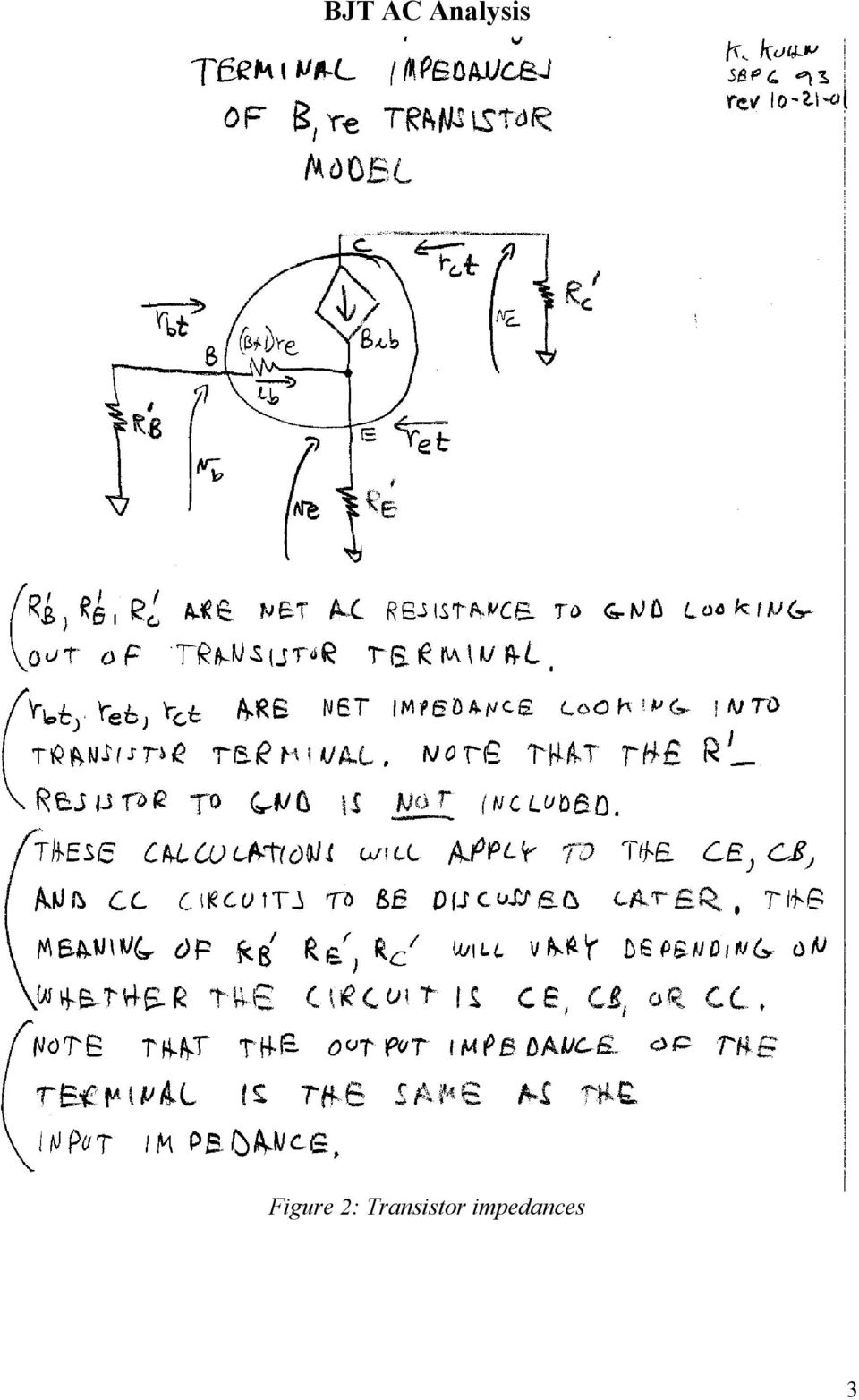
4 For the three types of amplifiers, R B, R E,and R C wil consist of external resistance combinations different for each amplifier type. In all cases, it should be obvious how to compute these resistances. Simply imagine yourself looking out of the specific transistor terminal and seeing the net AC resistance to ground. For example, for the commonemitter amplifier, R B may be the paralel combination of the voltage divider bias resistors, R B1 and R B2, also in parallel with R S since the coupling capacitor is an AC short. R E may be R E in parallel with R E1 for a common-emitter circuit or R E in parallel with R L in a common-collector circuit. R C may be R C in parallel with R L for commonemitter and common-base circuits. For the common-base circuit, R E is generaly just R E. The point is that no matter what the external circuit, it will be reduced to a single resistance representing the AC resistance. For this process, all coupling and bypass capacitors are treated as short circuits to AC which in fact they are at the signal frequencies we are using. The AC resistances looking into the terminals of the transistor are called r bt, r et, and r ct. Just to clarify the nomenclature, r bt is the AC resistance looking into the base terminal. Note that r bt does not include R B but is afected by R E, r et does not include R E but is affected by R B, and that r ct does not include R C. Calculation of r bt r bt = v b / i b by Ohms law Eq. 2 i b = (v b - v e ) / [(B + 1) * r e ] by inspection of the circuit Eq. 3 v e = (B + 1) * i b * R E by definition of transistor emitter current Eq. 4 v b = v e + i b * (B + 1) * r e by Kirchof s voltage law Eq. 5 v b = (B + 1) * i b * R E + i b * (B + 1) * r e by substituting equation for v e above Eq. 6 v b = (B + 1) * i b * (re + R E ) by combining terms Eq. 7 r bt = (B + 1) * (r e + R E ) dividing by i b produces Eq. 8 4

5 Calculation of r et r et = v e / (-i e ) By Ohm s law. Negative because i e is defined as positive for current leaving the emitter. We are looking in. Eq. 9 i e = (B + 1) * i b By definition Eq. 10 i b = -v e / [(B + 1) * r e + R B ] Notice that v e is across the sum of these two resistances Eq. 11 i e = (B + 1) *(-v e ) / [(B + 1) * r e + R B ] by combining the two previous equations Eq. 12 r et = [(B + 1) * r e + R B ] / (B + 1) By solving the above equation for r et Eq. 13 r et = r e + R B / (B + 1) Simplifying the above equation Eq. 14 Calculation of r ct r ct = v c / i c By Ohm s law Eq. 15 i c = 0 We note that i c = 0 because i b = 0 Eq. 16 r ct = infinity This should not be surprising since we are looking into a current source. A more complete model of the transistor would show that r ct is generally between about 30,000 and 1,000,000 Ohms. Eq. 17 The above analysis is very quick and may not be understood by all. If you have trouble understanding it then perform a two loop mesh analysis on the circuit in Figure 2 and the results should become more clear. Calculation of Input Resistance, Output Resistance, and Voltage Gain We are now ready to use r bt, r et, and r ct to perform specific AC analysis for each of the three types of amplifiers. Note that the impedance calculations can now be performed by inspection. We will do an analysis for each of the three amplifier types commonemitter, common-base, and common-collector. The circuits for these are in Figure 3. 5
![12 r et = [(B + 1) * r e + R B ] / (B + 1) By solving the above equation for r et Eq. 13 r et = r e + R B / (B + 1) Simplifying the above equation Eq.](/docs-images/46/21338709/images/page_5.jpg "14 Calculation of r ct r ct = v c / i c By Ohm s law Eq. 15 i c = 0 We note that i c = 0 because i b = 0 Eq.")
6 Figure 3: Transistor AC circuits 6
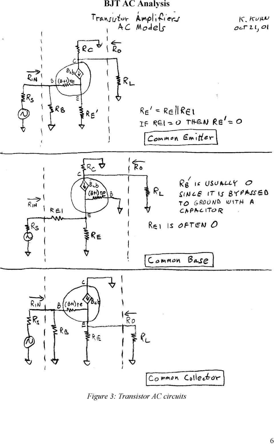
7 Common-Emitter analysis BJT AC Analysis r IN = R B r bt = R B [(B + 1) * (r e + R E )] Eq. 18 Note that R E = R E R E1. If R E1 is zero then R E is also zero. Eq. 19 r O = R C r ct = R C since for the beta, re model, r ct is taken to be infinity although real values are in the 30,000 to 1,000,000 Ohm range. Eq. 20 To find the voltage gain, we note that: v c = -i c * R C = -B * i b * R C = -B * [v b /[(B + 1) * (r e + R E )] * R C Eq. 21 Noting that voltage gain is v c /v b, then by rearranging the above equation we can write: -B R C Unloaded voltage gain = * Eq. 22 B + 1 r e + R E The voltage gain is negative because the output signal is inverted from the input signal. The output voltage division factor is R L / (R O + R L ). Using R O = R C, the -B R C R L Loaded voltage gain = * * Eq. 23 B + 1 r e + R E R C + R L The input voltage division factor is r IN / (R S + r IN ). The net voltage gain from the source to the load is: r IN -B R C R L Net voltage gain = * * * Eq. 24 R S + r IN B + 1 r e + R E R C + R L 7
 * (r e + R E )] * R C Eq.")
8 Common-Base Analysis BJT AC Analysis r IN = R E1 + R E r et = R E1 + R E [r e + R B /(B + 1)] Eq. 25 R B is often bypassed to ground using a capacitor that is a short circuit at the signal frequencies of interest. In that case R B is zero andthen: r IN = R E1 + R E r e Eq. 26 r O = R C r ct = R C Eq. 27 To find the gain we note that: v c = -i c * R C = -B * i b * R C = -B * (-i e / (B + 1)) * R C = (B / (B + 1)) * (v e / r e ) * R C Eq. 28 v e = v in * (r e R E ) / (R E1 + r e R E ) Eq. 29 Noting that gain is v c /v in we can write: 1 B R C Unloaded voltage gain = * * Eq. 30 R E1 / (r e R E ) + 1 B + 1 r e Considering the output voltage division we can write: 1 B R C R L Loaded voltage gain = * * * Eq. 31 R E1 / (r e R E ) + 1 B + 1 r e R C + R L Including the input voltage division factor, the net gain from signal source to output is: r IN 1 B R C R L Net voltage gain = * * * * Eq. 32 R S + r IN R E1 / (r e R E ) + 1 B + 1 r e R C + R L 8
 / (R E1 + r e R E ) Eq. 29 Noting that gain is v c /v in we can write: 1 B R C Unloaded voltage gain = -------------------- * -------- * ------ Eq.")
9 Common-Collector analysis BJT AC Analysis r IN = R B r bt = R B [(B + 1) * (r e + R E R L )] Eq. 33 Note that the input resistance is influenced by the load resistance. r O = R E r et = R E [r e + (R B R S )/(B + 1)] Eq. 34 Note that the output resistance is influenced by the source resistance. To calculate the unloaded gain we note that: v e = i e * R E = (B + 1) * i b * R E Eq. 35 i b = v b / [(B + 1) * (r e + R E )] Eq. 36 Solving Equations 34 and 35 for the ratio of v e to v b gives: v e R E Unloaded voltage gain = ---- = Eq. 37 v b r e + R E The influence that load impedance has on input resistance and the influence that source impedance has on output impedance leads to an algebraic mess when trying to calculate loaded gain. A better approach is to directly calculate loaded gain without using the usual output voltage division equation. By replacing R E with R E R L, we can directly calculate the loaded gain following the same procedure for unloaded gain. v e = i e * R E R L = (B + 1) * i b * R E R L Eq. 38 i b = v b / [(B + 1) * (r e + R E R L )] Eq. 39 v e R E R L Loaded voltage gain = = Eq. 40 v b r e + R E R L The net loaded gain from signal source to load is: r IN R E R L Net voltage gain = * Eq. 41 R S + r IN r e + R E R L 9
![To calculate the unloaded gain we note that: v e = i e * R E = (B + 1) * i b * R E Eq. 35 i b = v b / [(B + 1) * (r e + R E )] Eq.](/docs-images/46/21338709/images/page_9.jpg "36 Solving Equations 34 and 35 for the ratio of v e to v b gives: v e R E Unloaded voltage gain = ---- = ---------- Eq.")
Bipolar Junction Transistor Basics
 by Kenneth A. Kuhn Sept. 29, 2001, rev 1 Introduction A bipolar junction transistor (BJT) is a three layer semiconductor device with either NPN or PNP construction. Both constructions have the identical
Bipolar Junction Transistors
 Bipolar Junction Transistors Physical Structure & Symbols NPN Emitter (E) n-type Emitter region p-type Base region n-type Collector region Collector (C) B C Emitter-base junction (EBJ) Base (B) (a) Collector-base
Transistor Characteristics and Single Transistor Amplifier Sept. 8, 1997
 Physics 623 Transistor Characteristics and Single Transistor Amplifier Sept. 8, 1997 1 Purpose To measure and understand the common emitter transistor characteristic curves. To use the base current gain
The basic cascode amplifier consists of an input common-emitter (CE) configuration driving an output common-base (CB), as shown above.
 configuration driving an output common-base (CB), as shown above.") Cascode Amplifiers by Dennis L. Feucht Two-transistor combinations, such as the Darlington configuration, provide advantages over single-transistor amplifier stages. Another two-transistor combination
Cascode Amplifiers by Dennis L. Feucht Two-transistor combinations, such as the Darlington configuration, provide advantages over single-transistor amplifier stages. Another two-transistor combination
Physics 623 Transistor Characteristics and Single Transistor Amplifier Sept. 13, 2006
 Physics 623 Transistor Characteristics and Single Transistor Amplifier Sept. 13, 2006 1 Purpose To measure and understand the common emitter transistor characteristic curves. To use the base current gain
Series and Parallel Resistive Circuits
 Series and Parallel Resistive Circuits The configuration of circuit elements clearly affects the behaviour of a circuit. Resistors connected in series or in parallel are very common in a circuit and act
LAB VII. BIPOLAR JUNCTION TRANSISTOR CHARACTERISTICS
 LAB VII. BIPOLAR JUNCTION TRANSISTOR CHARACTERISTICS 1. OBJECTIVE In this lab, you will study the DC characteristics of a Bipolar Junction Transistor (BJT). 2. OVERVIEW You need to first identify the physical
BJT Characteristics and Amplifiers
 BJT Characteristics and Amplifiers Matthew Beckler beck0778@umn.edu EE2002 Lab Section 003 April 2, 2006 Abstract As a basic component in amplifier design, the properties of the Bipolar Junction Transistor
The 2N3393 Bipolar Junction Transistor
 The 2N3393 Bipolar Junction Transistor Common-Emitter Amplifier Aaron Prust Abstract The bipolar junction transistor (BJT) is a non-linear electronic device which can be used for amplification and switching.
LAB VIII. BIPOLAR JUNCTION TRANSISTOR CHARACTERISTICS
 LAB VIII. BIPOLAR JUNCTION TRANSISTOR CHARACTERISTICS 1. OBJECTIVE In this lab, you will study the DC characteristics of a Bipolar Junction Transistor (BJT). 2. OVERVIEW In this lab, you will inspect the
Fig6-22 CB configuration. Z i [6-54] Z o [6-55] A v [6-56] Assuming R E >> r e. A i [6-57]
![Fig6-22 CB configuration. Z i [6-54] Z o [6-55] A v [6-56] Assuming R E >> r e. A i [6-57]](/thumbs/40/21338705.jpg "Fig6-22 CB configuration. Z i [6-54] Z o [6-55] A v [6-56] Assuming R E >> r e. A i [6-57]") Common-Base Configuration (CB) The CB configuration having a low input and high output impedance and a current gain less than 1, the voltage gain can be quite large, r o in MΩ so that ignored in parallel
Common-Base Configuration (CB) The CB configuration having a low input and high output impedance and a current gain less than 1, the voltage gain can be quite large, r o in MΩ so that ignored in parallel
http://users.ece.gatech.edu/~mleach/ece3050/notes/feedback/fbexamples.pdf
 c Copyright 2009. W. Marshall Leach, Jr., Professor, Georgia Institute of Technology, School of Electrical and Computer Engineering. Feedback Amplifiers CollectionofSolvedProblems A collection of solved
Transistor Amplifiers
 Physics 3330 Experiment #7 Fall 1999 Transistor Amplifiers Purpose The aim of this experiment is to develop a bipolar transistor amplifier with a voltage gain of minus 25. The amplifier must accept input
Common-Emitter Amplifier
 Common-Emitter Amplifier A. Before We Start As the title of this lab says, this lab is about designing a Common-Emitter Amplifier, and this in this stage of the lab course is premature, in my opinion,
BJT Amplifier Circuits
 JT Amplifier ircuits As we have developed different models for D signals (simple large-signal model) and A signals (small-signal model), analysis of JT circuits follows these steps: D biasing analysis:
Basic Electronics Prof. Dr. Chitralekha Mahanta Department of Electronics and Communication Engineering Indian Institute of Technology, Guwahati
 Basic Electronics Prof. Dr. Chitralekha Mahanta Department of Electronics and Communication Engineering Indian Institute of Technology, Guwahati Module: 2 Bipolar Junction Transistors Lecture-2 Transistor
MAS.836 HOW TO BIAS AN OP-AMP
 MAS.836 HOW TO BIAS AN OP-AMP Op-Amp Circuits: Bias, in an electronic circuit, describes the steady state operating characteristics with no signal being applied. In an op-amp circuit, the operating characteristic
Bipolar Transistor Amplifiers
 Physics 3330 Experiment #7 Fall 2005 Bipolar Transistor Amplifiers Purpose The aim of this experiment is to construct a bipolar transistor amplifier with a voltage gain of minus 25. The amplifier must
Common Emitter BJT Amplifier Design Current Mirror Design
 Common Emitter BJT Amplifier Design Current Mirror Design 1 Some Random Observations Conditions for stabilized voltage source biasing Emitter resistance, R E, is needed. Base voltage source will have finite
Figure 1: Common-base amplifier.
 The Common-Base Amplifier Basic Circuit Fig. 1 shows the circuit diagram of a single stage common-base amplifier. The object is to solve for the small-signal voltage gain, input resistance, and output
BJT AC Analysis 1 of 38. The r e Transistor model. Remind Q-poiint re = 26mv/IE
 BJT AC Analysis 1 of 38 The r e Transistor model Remind Q-poiint re = 26mv/IE BJT AC Analysis 2 of 38 Three amplifier configurations, Common Emitter Common Collector (Emitter Follower) Common Base BJT
BJT Amplifier Circuits
 JT Amplifier ircuits As we have developed different models for D signals (simple large-signal model) and A signals (small-signal model), analysis of JT circuits follows these steps: D biasing analysis:
Series and Parallel Circuits
 Direct Current (DC) Direct current (DC) is the unidirectional flow of electric charge. The term DC is used to refer to power systems that use refer to the constant (not changing with time), mean (average)
BIPOLAR JUNCTION TRANSISTORS
 CHAPTER 3 BIPOLAR JUNCTION TRANSISTORS A bipolar junction transistor, BJT, is a single piece of silicon with two back-to-back P-N junctions. However, it cannot be made with two independent back-to-back
Lecture-7 Bipolar Junction Transistors (BJT) Part-I Continued
 Part-I Continued") 1 Lecture-7 ipolar Junction Transistors (JT) Part-I ontinued 1. ommon-emitter (E) onfiguration: Most JT circuits employ the common-emitter configuration shown in Fig.1. This is due mainly to the fact that
1 Lecture-7 ipolar Junction Transistors (JT) Part-I ontinued 1. ommon-emitter (E) onfiguration: Most JT circuits employ the common-emitter configuration shown in Fig.1. This is due mainly to the fact that
Differential Amplifier Offset. Causes of dc voltage and current offset Modeling dc offset R C
 ESE39 ntroduction to Microelectronics Differential Amplifier Offset Causes of dc voltage and current offset Modeling dc offset mismatch S mismatch β mismatch transistor mismatch dc offsets in differential
VI. Transistor amplifiers: Biasing and Small Signal Model
 VI. Transistor amplifiers: iasing and Small Signal Model 6.1 Introduction Transistor amplifiers utilizing JT or FET are similar in design and analysis. Accordingly we will discuss JT amplifiers thoroughly.
CIRCUITS LABORATORY. In this experiment, the output I-V characteristic curves, the small-signal low
 CIRCUITS LABORATORY EXPERIMENT 6 TRANSISTOR CHARACTERISTICS 6.1 ABSTRACT In this experiment, the output I-V characteristic curves, the small-signal low frequency equivalent circuit parameters, and the
Lecture 12: DC Analysis of BJT Circuits.
 Whites, 320 Lecture 12 Page 1 of 9 Lecture 12: D Analysis of JT ircuits. n this lecture we will consider a number of JT circuits and perform the D circuit analysis. For those circuits with an active mode
Differential transistor amplifiers
 Differential transistor amplifiers This worksheet and all related files are licensed under the Creative Commons Attribution License, version 1.0. To view a copy of this license, visit http://creativecommons.org/licenses/by/1.0/,
Objectives The purpose of this lab is build and analyze Differential amplifiers based on NPN transistors (or NMOS transistors).
.") 1 Lab 03: Differential Amplifiers (BJT) (20 points) NOTE: 1) Please use the basic current mirror from Lab01 for the second part of the lab (Fig. 3). 2) You can use the same chip as the basic current mirror;
1 Lab 03: Differential Amplifiers (BJT) (20 points) NOTE: 1) Please use the basic current mirror from Lab01 for the second part of the lab (Fig. 3). 2) You can use the same chip as the basic current mirror;
BIASING OF CONSTANT CURRENT MMIC AMPLIFIERS (e.g., ERA SERIES) (AN-60-010)
 (AN-60-010)") BIASING OF CONSTANT CURRENT MMIC AMPLIFIERS (e.g., ERA SERIES) (AN-60-010) Introduction The Mini-Circuits family of microwave monolithic integrated circuit (MMIC) Darlington amplifiers offers the RF designer
BIASING OF CONSTANT CURRENT MMIC AMPLIFIERS (e.g., ERA SERIES) (AN-60-010) Introduction The Mini-Circuits family of microwave monolithic integrated circuit (MMIC) Darlington amplifiers offers the RF designer
PROCEDURE: 1. Measure and record the actual values of the four resistors listed in Table 10-1.
 The answer to two questions will help you identify a series or parallel connection: (1) Will the identical current go through both components? f the answer is yes, the components are in series. (2) Are
Scaling and Biasing Analog Signals
 Scaling and Biasing Analog Signals November 2007 Introduction Scaling and biasing the range and offset of analog signals is a useful skill for working with a variety of electronics. Not only can it interface
Transistors. NPN Bipolar Junction Transistor
 Transistors They are unidirectional current carrying devices with capability to control the current flowing through them The switch current can be controlled by either current or voltage ipolar Junction
W03 Analysis of DC Circuits. Yrd. Doç. Dr. Aytaç Gören
 W03 Analysis of DC Circuits Yrd. Doç. Dr. Aytaç Gören ELK 2018 - Contents W01 Basic Concepts in Electronics W02 AC to DC Conversion W03 Analysis of DC Circuits (self and condenser) W04 Transistors and
AMPLIFIERS BJT BJT TRANSISTOR. Types of BJT BJT. devices that increase the voltage, current, or power level
 AMPLFERS Prepared by Engr. JP Timola Reference: Electronic Devices by Floyd devices that increase the voltage, current, or power level have at least three terminals with one controlling the flow between
Kirchhoff's Current Law (KCL)
") Kirchhoff's Current Law (KCL) I. Charge (current flow) conservation law (the Kirchhoff s Current law) Pipe Pipe Pipe 3 Total volume of water per second flowing through pipe = total volume of water per
Kirchhoff's Current Law (KCL) I. Charge (current flow) conservation law (the Kirchhoff s Current law) Pipe Pipe Pipe 3 Total volume of water per second flowing through pipe = total volume of water per
Chapter 12: The Operational Amplifier
 Chapter 12: The Operational Amplifier 12.1: Introduction to Operational Amplifier (Op-Amp) Operational amplifiers (op-amps) are very high gain dc coupled amplifiers with differential inputs; they are used
= (0.400 A) (4.80 V) = 1.92 W = (0.400 A) (7.20 V) = 2.88 W
 (4.80 V) = 1.92 W = (0.400 A) (7.20 V) = 2.88 W") Physics 2220 Module 06 Homework 0. What are the magnitude and direction of the current in the 8 Ω resister in the figure? Assume the current is moving clockwise. Then use Kirchhoff's second rule: 3.00
Physics 2220 Module 06 Homework 0. What are the magnitude and direction of the current in the 8 Ω resister in the figure? Assume the current is moving clockwise. Then use Kirchhoff's second rule: 3.00
LM 358 Op Amp. If you have small signals and need a more useful reading we could amplify it using the op amp, this is commonly used in sensors.
 LM 358 Op Amp S k i l l L e v e l : I n t e r m e d i a t e OVERVIEW The LM 358 is a duel single supply operational amplifier. As it is a single supply it eliminates the need for a duel power supply, thus
Lecture 18: Common Emitter Amplifier. Maximum Efficiency of Class A Amplifiers. Transformer Coupled Loads.
 Whites, EE 3 Lecture 18 Page 1 of 10 Lecture 18: Common Emitter Amplifier. Maximum Efficiency of Class A Amplifiers. Transformer Coupled Loads. We discussed using transistors as switches in the last lecture.
LABORATORY 2 THE DIFFERENTIAL AMPLIFIER
 LABORATORY 2 THE DIFFERENTIAL AMPLIFIER OBJECTIVES 1. To understand how to amplify weak (small) signals in the presence of noise. 1. To understand how a differential amplifier rejects noise and common
Common Base BJT Amplifier Common Collector BJT Amplifier
 Common Base BJT Amplifier Common Collector BJT Amplifier Common Collector (Emitter Follower) Configuration Common Base Configuration Small Signal Analysis Design Example Amplifier Input and Output Impedances
05 Bipolar Junction Transistors (BJTs) basics
 basics") The first bipolar transistor was realized in 1947 by Brattain, Bardeen and Shockley. The three of them received the Nobel prize in 1956 for their invention. The bipolar transistor is composed of two PN
The first bipolar transistor was realized in 1947 by Brattain, Bardeen and Shockley. The three of them received the Nobel prize in 1956 for their invention. The bipolar transistor is composed of two PN
A Comparison of Various Bipolar Transistor Biasing Circuits Application Note 1293
 A omparison of Various Bipolar Transistor Biasing ircuits Application Note 1293 Introduction The bipolar junction transistor (BJT) is quite often used as a low noise amplifier in cellular, PS, and pager
Content Map For Career & Technology
 Content Strand: Applied Academics CT-ET1-1 analysis of electronic A. Fractions and decimals B. Powers of 10 and engineering notation C. Formula based problem solutions D. Powers and roots E. Linear equations
Basic Op Amp Circuits
 Basic Op Amp ircuits Manuel Toledo INEL 5205 Instrumentation August 3, 2008 Introduction The operational amplifier (op amp or OA for short) is perhaps the most important building block for the design of
Diode Circuits. Operating in the Reverse Breakdown region. (Zener Diode)
") Diode Circuits Operating in the Reverse Breakdown region. (Zener Diode) In may applications, operation in the reverse breakdown region is highly desirable. The reverse breakdown voltage is relatively insensitive
Diode Circuits Operating in the Reverse Breakdown region. (Zener Diode) In may applications, operation in the reverse breakdown region is highly desirable. The reverse breakdown voltage is relatively insensitive
Without the pre amp, these microphones sound very good with tube equipment that provided a very high impedance load to the element.
 N9WB D-104 Project Revision 2 Pre Amp Modifications for higher load impedance. By Walter A. Breining, N9WB D-104 Discussion The D-104 has been around since the 30 s and is still popular today for communications.
WHY DIFFERENTIAL? instruments connected to the circuit under test and results in V COMMON.
 WHY DIFFERENTIAL? Voltage, The Difference Whether aware of it or not, a person using an oscilloscope to make any voltage measurement is actually making a differential voltage measurement. By definition,
Bipolar transistor biasing circuits
 Bipolar transistor biasing circuits This worksheet and all related files are licensed under the Creative Commons Attribution License, version 1.0. To view a copy of this license, visit http://creativecommons.org/licenses/by/1.0/,
Lab 7: Operational Amplifiers Part I
 Lab 7: Operational Amplifiers Part I Objectives The objective of this lab is to study operational amplifier (op amp) and its applications. We will be simulating and building some basic op amp circuits,
Collection of Solved Feedback Amplifier Problems
 c Copyright 2009. W. Marshall Leach, Jr., Professor, Georgia Institute of Technology, School of Electrical and Computer Engineering. Collection of Solved Feedback Amplifier Problems This document contains
Chapter 8 Differential and Multistage Amplifiers. EE 3120 Microelectronics II
 1 Chapter 8 Differential and Multistage Amplifiers Operational Amplifier Circuit Components 2 1. Ch 7: Current Mirrors and Biasing 2. Ch 9: Frequency Response 3. Ch 8: Active-Loaded Differential Pair 4.
30. Bode Plots. Introduction
 0. Bode Plots Introduction Each of the circuits in this problem set is represented by a magnitude Bode plot. The network function provides a connection between the Bode plot and the circuit. To solve these
3.4 - BJT DIFFERENTIAL AMPLIFIERS
 BJT Differential Amplifiers (6/4/00) Page 1 3.4 BJT DIFFERENTIAL AMPLIFIERS INTRODUCTION Objective The objective of this presentation is: 1.) Define and characterize the differential amplifier.) Show the
Electronics. Discrete assembly of an operational amplifier as a transistor circuit. LD Physics Leaflets P4.2.1.1
 Electronics Operational Amplifier Internal design of an operational amplifier LD Physics Leaflets Discrete assembly of an operational amplifier as a transistor circuit P4.2.1.1 Objects of the experiment
Measurement of Capacitance
 Measurement of Capacitance Pre-Lab Questions Page Name: Class: Roster Number: Instructor:. A capacitor is used to store. 2. What is the SI unit for capacitance? 3. A capacitor basically consists of two
TWO PORT NETWORKS h-parameter BJT MODEL
 TWO PORT NETWORKS h-parameter BJT MODEL The circuit of the basic two port network is shown on the right. Depending on the application, it may be used in a number of different ways to develop different
Precision Diode Rectifiers
 by Kenneth A. Kuhn March 21, 2013 Precision half-wave rectifiers An operational amplifier can be used to linearize a non-linear function such as the transfer function of a semiconductor diode. The classic
LM2576R. 3.0A, 52kHz, Step-Down Switching Regulator FEATURES. Applications DESCRIPTION TO-220 PKG TO-220V PKG TO-263 PKG ORDERING INFORMATION
 LM2576 FEATURES 3.3, 5.0, 12, 15, and Adjustable Output ersions Adjustable ersion Output oltage Range, 1.23 to 37 +/- 4% AG10Maximum Over Line and Load Conditions Guaranteed 3.0A Output Current Wide Input
Transistor amplifiers: Biasing and Small Signal Model
 Transistor amplifiers: iasing and Small Signal Model Transistor amplifiers utilizing JT or FT are similar in design and analysis. Accordingly we will discuss JT amplifiers thoroughly. Then, similar FT
SIMULATIONS OF PARALLEL RESONANT CIRCUIT POWER ELECTRONICS COLORADO STATE UNIVERSITY
 SIMULATIONS OF PARALLEL RESONANT CIRCUIT POWER ELECTRONICS COLORADO STATE UNIVERSITY Page 1 of 25 PURPOSE: The purpose of this lab is to simulate the LCC circuit using MATLAB and ORCAD Capture CIS to better
Operational Amplifier - IC 741
 Operational Amplifier - IC 741 Tabish December 2005 Aim: To study the working of an 741 operational amplifier by conducting the following experiments: (a) Input bias current measurement (b) Input offset
Superposition Examples
 Superposition Examples The following examples illustrate the proper use of superposition of dependent sources. All superposition equations are written by inspection using voltage division, current division,
Student Exploration: Circuits
 Name: Date: Student Exploration: Circuits Vocabulary: ammeter, circuit, current, ohmmeter, Ohm s law, parallel circuit, resistance, resistor, series circuit, voltage Prior Knowledge Questions (Do these
Transistor Biasing. The basic function of transistor is to do amplification. Principles of Electronics
 192 9 Principles of Electronics Transistor Biasing 91 Faithful Amplification 92 Transistor Biasing 93 Inherent Variations of Transistor Parameters 94 Stabilisation 95 Essentials of a Transistor Biasing
Chapter 24. Three-Phase Voltage Generation
 Chapter 24 Three-Phase Systems Three-Phase Voltage Generation Three-phase generators Three sets of windings and produce three ac voltages Windings are placed 120 apart Voltages are three identical sinusoidal
POWER SUPPLY MODEL XP-15. Instruction Manual ELENCO
 POWER SUPPLY MODEL XP-15 Instruction Manual ELENCO Copyright 2013 by Elenco Electronics, Inc. REV-A 753020 All rights reserved. No part of this book shall be reproduced by any means; electronic, photocopying,
V out. Figure 1: A voltage divider on the left, and potentiometer on the right.
 Living with the Lab Fall 202 Voltage Dividers and Potentiometers Gerald Recktenwald v: November 26, 202 gerry@me.pdx.edu Introduction Voltage dividers and potentiometers are passive circuit components
Lecture 21: Junction Field Effect Transistors. Source Follower Amplifier
 Whites, EE 322 Lecture 21 Page 1 of 8 Lecture 21: Junction Fiel Effect Transistors. Source Follower Amplifier As mentione in Lecture 16, there are two major families of transistors. We ve worke with BJTs
GenTech Practice Questions
 GenTech Practice Questions Basic Electronics Test: This test will assess your knowledge of and ability to apply the principles of Basic Electronics. This test is comprised of 90 questions in the following
Basic Laws Circuit Theorems Methods of Network Analysis Non-Linear Devices and Simulation Models
 EE Modul 1: Electric Circuits Theory Basic Laws Circuit Theorems Methods of Network Analysis Non-Linear Devices and Simulation Models EE Modul 1: Electric Circuits Theory Current, Voltage, Impedance Ohm
Application Note 142 August 2013. New Linear Regulators Solve Old Problems AN142-1
 August 2013 New Linear Regulators Solve Old Problems Bob Dobkin, Vice President, Engineering and CTO, Linear Technology Corp. Regulators regulate but are capable of doing much more. The architecture of
Reading: HH Sections 4.11 4.13, 4.19 4.20 (pgs. 189-212, 222 224)
") 6 OP AMPS II 6 Op Amps II In the previous lab, you explored several applications of op amps. In this exercise, you will look at some of their limitations. You will also examine the op amp integrator and
6 OP AMPS II 6 Op Amps II In the previous lab, you explored several applications of op amps. In this exercise, you will look at some of their limitations. You will also examine the op amp integrator and
Inductors in AC Circuits
 Inductors in AC Circuits Name Section Resistors, inductors, and capacitors all have the effect of modifying the size of the current in an AC circuit and the time at which the current reaches its maximum
6.101 Final Project Report Class G Audio Amplifier
 6.101 Final Project Report Class G Audio Amplifier Mark Spatz 4/3/2014 1 1 Introduction For my final project, I designed and built a 150 Watt audio amplifier to replace the underpowered and unreliable
Operating Manual Ver.1.1
 Class B Amplifier (Push-Pull Emitter Follower) Operating Manual Ver.1.1 An ISO 9001 : 2000 company 94-101, Electronic Complex Pardesipura, Indore- 452010, India Tel : 91-731- 2570301/02, 4211100 Fax: 91-731-
Tristan s Guide to: Solving Parallel Circuits. Version: 1.0 Written in 2006. Written By: Tristan Miller Tristan@CatherineNorth.com
 Tristan s Guide to: Solving Parallel Circuits. Version: 1.0 Written in 2006 Written By: Tristan Miller Tristan@CatherineNorth.com Parallel Circuits. Parallel Circuits are a little bit more complicated
Chapter 19 Operational Amplifiers
 Chapter 19 Operational Amplifiers The operational amplifier, or op-amp, is a basic building block of modern electronics. Op-amps date back to the early days of vacuum tubes, but they only became common
Experiment 4 ~ Resistors in Series & Parallel
 Experiment 4 ~ Resistors in Series & Parallel Objective: In this experiment you will set up three circuits: one with resistors in series, one with resistors in parallel, and one with some of each. You
Preamble. Kirchoff Voltage Law (KVL) Series Resistors. In this section of my lectures we will be. resistor arrangements; series and
 Series Resistors. In this section of my lectures we will be. resistor arrangements; series and") Preamble Series and Parallel Circuits Physics, 8th Edition Custom Edition Cutnell & Johnson Chapter 0.6-0.8, 0.0 Pages 60-68, 69-6 n this section of my lectures we will be developing the two common types
Preamble Series and Parallel Circuits Physics, 8th Edition Custom Edition Cutnell & Johnson Chapter 0.6-0.8, 0.0 Pages 60-68, 69-6 n this section of my lectures we will be developing the two common types
Lecture 30: Biasing MOSFET Amplifiers. MOSFET Current Mirrors.
 Whites, EE 320 Lecture 30 Page 1 of 8 Lecture 30: Biasing MOSFET Amplifiers. MOSFET Current Mirrors. There are two different environments in which MOSFET amplifiers are found, (1) discrete circuits and
5B5BBasic RC Oscillator Circuit
 5B5BBasic RC Oscillator Circuit The RC Oscillator which is also called a Phase Shift Oscillator, produces a sine wave output signal using regenerative feedback from the resistor-capacitor combination.
Building the AMP Amplifier
 Building the AMP Amplifier Introduction For about 80 years it has been possible to amplify voltage differences and to increase the associated power, first with vacuum tubes using electrons from a hot filament;
Transistor Models. ampel
 Transistor Models Review of Transistor Fundamentals Simple Current Amplifier Model Transistor Switch Example Common Emitter Amplifier Example Transistor as a Transductance Device - Ebers-Moll Model Other
Positive Feedback and Oscillators
 Physics 3330 Experiment #6 Fall 1999 Positive Feedback and Oscillators Purpose In this experiment we will study how spontaneous oscillations may be caused by positive feedback. You will construct an active
Unit/Standard Number. High School Graduation Years 2010, 2011 and 2012
 1 Secondary Task List 100 SAFETY 101 Demonstrate an understanding of State and School safety regulations. 102 Practice safety techniques for electronics work. 103 Demonstrate an understanding of proper
Experiment NO.3 Series and parallel connection
 Experiment NO.3 Series and parallel connection Object To study the properties of series and parallel connection. Apparatus 1. DC circuit training system 2. Set of wires. 3. DC Power supply 4. Digital A.V.O.
Operational Amplifiers
 Module 6 Amplifiers Operational Amplifiers The Ideal Amplifier What you ll learn in Module 6. Section 6.0. Introduction to Operational Amplifiers. Understand Concept of the Ideal Amplifier and the Need
RLC Resonant Circuits
 C esonant Circuits Andrew McHutchon April 20, 203 Capacitors and Inductors There is a lot of inconsistency when it comes to dealing with reactances of complex components. The format followed in this document
Homework Assignment 03
 Question 1 (2 points each unless noted otherwise) Homework Assignment 03 1. A 9-V dc power supply generates 10 W in a resistor. What peak-to-peak amplitude should an ac source have to generate the same
The BJT Differential Amplifier. Basic Circuit. DC Solution
 c Copyright 010. W. Marshall Leach, Jr., Professor, Georgia Institute of Technology, School of Electrical and Computer Engineering. The BJT Differential Amplifier Basic Circuit Figure 1 shows the circuit
Power Amplifiers. Introduction to Power Amplifiers. Amplifiers. Module 5
 Module 5 Amplifiers Introduction to What you ll learn in Module 5. Section 5.0 Introduction to. Understand the Operation of. Section 5.1 Power Transistors & Heat Sinks. Power Transistor Construction. Power
A Short Discussion on Summing Busses and Summing Amplifiers By Fred Forssell Copyright 2001, by Forssell Technologies All Rights Reserved
 A Short Discussion on Summing Busses and Summing Amplifiers By Fred Forssell Copyright 2001, by Forssell Technologies All Rights Reserved The summing network in mixing consoles is an easily misunderstood
Parallel and Series Resistors, Kirchoff s Law
 Experiment 2 31 Kuwait University Physics 107 Physics Department Parallel and Series Resistors, Kirchoff s Law Introduction In this experiment the relations among voltages, currents and resistances for
Impedance Matching and Matching Networks. Valentin Todorow, December, 2009
 Impedance Matching and Matching Networks Valentin Todorow, December, 2009 RF for Plasma Processing - Definition of RF What is RF? The IEEE Standard Dictionary of Electrical and Electronics Terms defines
Gates, Circuits, and Boolean Algebra
 Gates, Circuits, and Boolean Algebra Computers and Electricity A gate is a device that performs a basic operation on electrical signals Gates are combined into circuits to perform more complicated tasks