Bipolar Junction Transistor Basics
|
|
|
- Henry Short
- 7 years ago
- Views:
Transcription
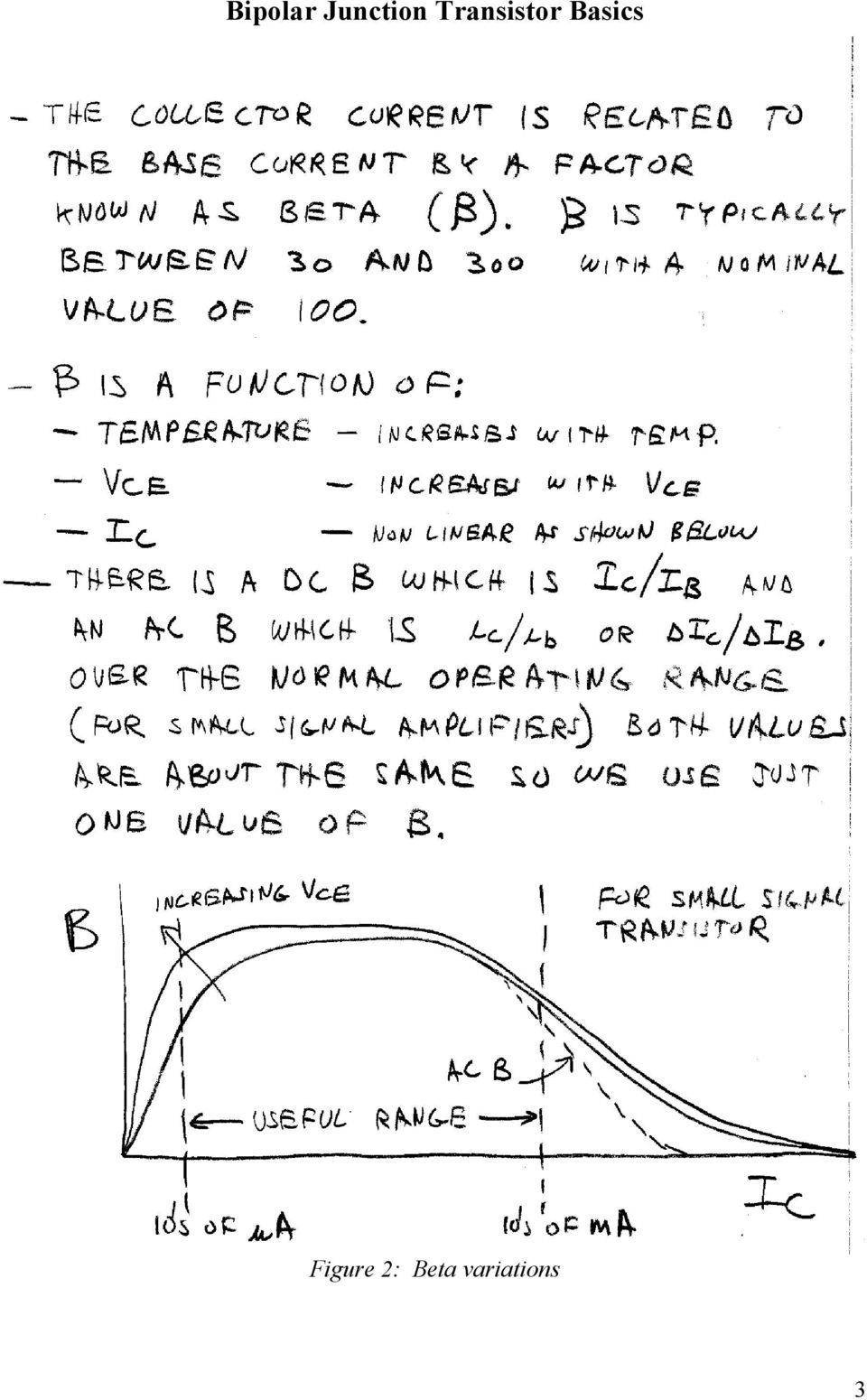
1 by Kenneth A. Kuhn Sept. 29, 2001, rev 1 Introduction A bipolar junction transistor (BJT) is a three layer semiconductor device with either NPN or PNP construction. Both constructions have the identical mathematical model but differ in that the terminal currents are inverted from each other. There are three terminals described as follows: Base Emitter Collector the control terminal the source of majority carriers the collector of majority carriers The basic mathematical model of the BJT is a current controlled current source. A current between the base and emitter terminals controls a current between the collector and emitter terminals. The name for the control factor is beta. The symbol for beta is β although B is often used too. The collector current is the base current multiplied by beta. The beta for typical small signal BJTs ranges from about 50 to 300. For linear amplifiers the base-emitter junction is always forward biased and the basecollector junction is always reversed biased. All of the math we use is based on this and will produce incorrect results if either condition is not true. An amplifier is based on a small base-emitter current controlling a much larger collector-emitter current. Although we treat beta as if it were a constant, we must keep in mind that beta is a complex function of temperature, collector current, and collector to emitter voltage. At first it would seem that it would be difficult to design a BJT circuit since the exact value of beta is not known for a particular transistor other than roughly the broad range described above. But, with proper design techniques, the bias design for a BJT circuit can be made to be very independent of beta. Figure 1 shows the construction and schematic symbols of NPN and PNP structures. The plots at the bottom show a family of characteristic curves. Linear operation is in the current saturation region as shown on the plots. In this region the collector current is very independent of the voltage across the transistor thus the name, current saturation. At very low voltages across the transistor the collector current has a strong dependency on voltage thus the name, ohmic region. Figure 2 shows how beta varies with temperature, voltage, and current through the transistor. Note that there is a DC beta (I C / I B ) term and an AC beta (ΔI C / ΔI B ) term. For most normal cases these two values are practically identical and for this course we will not make a distinction. 1

2 Figure 1: Basic transistor characteristics 2

3 Figure 2: Beta variations 3
4 Transistor Nomenclature Bipolar Junction Transistor Basics Figure 3 illustrates standard transistor nomenclature. Note that DC values are in upper case and AC or signal values are in lower case. This is done because there is a significant difference between the DC and AC solution. We always calculate the DC or bias solution first and then that result is used to calculate the AC or signal characteristics. It is very important to note that the signal is generally a small value compared to the corresponding bias value Transistor Equations Here are the two fundamental bipolar transistor equations for linear circuit analysis. Everything we do with bipolar transistors is based on these two equations. I C = B * I B I E = I B + I C The collector current is controlled by the base current The emitter current is the sum of the base and collector currents The following equations are derived from the first two (The student should become proficient at deriving these). I B = I C / B I E = (B + 1) * I B I B = I E / (B + 1) I C = (B / (B + 1)) * I E Note that B/(B+1) is always slightly less than 1 I E = ((B + 1) / B) * I C Note that (B+1)/B is always slightly greater than 1 The following is a summary of all the possible permutations of the above equations. The student should develop the ability to quickly derive all of them. It is very important to note that these equations only apply if the transistor is being operated in the current saturation region (i.e. linear region for building amplifiers). These equations do not apply in the ohmic region. Known Unknown I C I B I E I C = * B * I B (B / (B + 1)) * I E I B = I C /B * I E / (B + 1) I E = ((B + 1) / B) * I C (B + 1) * I B * 4

5 Figure 3: Transistor nomenclature 5

LAB VII. BIPOLAR JUNCTION TRANSISTOR CHARACTERISTICS
 LAB VII. BIPOLAR JUNCTION TRANSISTOR CHARACTERISTICS 1. OBJECTIVE In this lab, you will study the DC characteristics of a Bipolar Junction Transistor (BJT). 2. OVERVIEW You need to first identify the physical
AMPLIFIERS BJT BJT TRANSISTOR. Types of BJT BJT. devices that increase the voltage, current, or power level
 AMPLFERS Prepared by Engr. JP Timola Reference: Electronic Devices by Floyd devices that increase the voltage, current, or power level have at least three terminals with one controlling the flow between
BJT AC Analysis. by Kenneth A. Kuhn Oct. 20, 2001, rev Aug. 31, 2008
 by Kenneth A. Kuhn Oct. 20, 2001, rev Aug. 31, 2008 Introduction This note will discuss AC analysis using the beta, re transistor model shown in Figure 1 for the three types of amplifiers: common-emitter,
Lecture 17. Bipolar Junction Transistors (BJT): Part 1 Qualitative Understanding - How do they work? Reading: Pierret 10.1-10.6, 11.
: Part 1 Qualitative Understanding - How do they work? Reading: Pierret 10.1-10.6, 11.") Lecture 17 Bipolar Junction Transistors (BJT): Part 1 Qualitative Understanding - How do they work? Reading: Pierret 10.1-10.6, 11.1 Looks sort of like two diodes back to back pnp mnemonic: Pouring N Pot
Lecture 17 Bipolar Junction Transistors (BJT): Part 1 Qualitative Understanding - How do they work? Reading: Pierret 10.1-10.6, 11.1 Looks sort of like two diodes back to back pnp mnemonic: Pouring N Pot
Basic Electronics Prof. Dr. Chitralekha Mahanta Department of Electronics and Communication Engineering Indian Institute of Technology, Guwahati
 Basic Electronics Prof. Dr. Chitralekha Mahanta Department of Electronics and Communication Engineering Indian Institute of Technology, Guwahati Module: 2 Bipolar Junction Transistors Lecture-2 Transistor
Bipolar Junction Transistors
 Bipolar Junction Transistors Physical Structure & Symbols NPN Emitter (E) n-type Emitter region p-type Base region n-type Collector region Collector (C) B C Emitter-base junction (EBJ) Base (B) (a) Collector-base
Transistor Characteristics and Single Transistor Amplifier Sept. 8, 1997
 Physics 623 Transistor Characteristics and Single Transistor Amplifier Sept. 8, 1997 1 Purpose To measure and understand the common emitter transistor characteristic curves. To use the base current gain
LAB VIII. BIPOLAR JUNCTION TRANSISTOR CHARACTERISTICS
 LAB VIII. BIPOLAR JUNCTION TRANSISTOR CHARACTERISTICS 1. OBJECTIVE In this lab, you will study the DC characteristics of a Bipolar Junction Transistor (BJT). 2. OVERVIEW In this lab, you will inspect the
CIRCUITS LABORATORY. In this experiment, the output I-V characteristic curves, the small-signal low
 CIRCUITS LABORATORY EXPERIMENT 6 TRANSISTOR CHARACTERISTICS 6.1 ABSTRACT In this experiment, the output I-V characteristic curves, the small-signal low frequency equivalent circuit parameters, and the
Transistors. NPN Bipolar Junction Transistor
 Transistors They are unidirectional current carrying devices with capability to control the current flowing through them The switch current can be controlled by either current or voltage ipolar Junction
Physics 623 Transistor Characteristics and Single Transistor Amplifier Sept. 13, 2006
 Physics 623 Transistor Characteristics and Single Transistor Amplifier Sept. 13, 2006 1 Purpose To measure and understand the common emitter transistor characteristic curves. To use the base current gain
BJT Characteristics and Amplifiers
 BJT Characteristics and Amplifiers Matthew Beckler beck0778@umn.edu EE2002 Lab Section 003 April 2, 2006 Abstract As a basic component in amplifier design, the properties of the Bipolar Junction Transistor
Bipolar Transistor Amplifiers
 Physics 3330 Experiment #7 Fall 2005 Bipolar Transistor Amplifiers Purpose The aim of this experiment is to construct a bipolar transistor amplifier with a voltage gain of minus 25. The amplifier must
Transistor Amplifiers
 Physics 3330 Experiment #7 Fall 1999 Transistor Amplifiers Purpose The aim of this experiment is to develop a bipolar transistor amplifier with a voltage gain of minus 25. The amplifier must accept input
BIPOLAR JUNCTION TRANSISTORS
 CHAPTER 3 BIPOLAR JUNCTION TRANSISTORS A bipolar junction transistor, BJT, is a single piece of silicon with two back-to-back P-N junctions. However, it cannot be made with two independent back-to-back
Lecture 17 The Bipolar Junction Transistor (I) Forward Active Regime
 Forward Active Regime") Lecture 17 The Bipolar Junction Transistor (I) Forward Active Regime Outline The Bipolar Junction Transistor (BJT): structure and basic operation I-V characteristics in forward active regime Reading Assignment:
Lecture 17 The Bipolar Junction Transistor (I) Forward Active Regime Outline The Bipolar Junction Transistor (BJT): structure and basic operation I-V characteristics in forward active regime Reading Assignment:
Diodes and Transistors
 Diodes What do we use diodes for? Diodes and Transistors protect circuits by limiting the voltage (clipping and clamping) turn AC into DC (voltage rectifier) voltage multipliers (e.g. double input voltage)
Unit/Standard Number. High School Graduation Years 2010, 2011 and 2012
 1 Secondary Task List 100 SAFETY 101 Demonstrate an understanding of State and School safety regulations. 102 Practice safety techniques for electronics work. 103 Demonstrate an understanding of proper
Transistor Models. ampel
 Transistor Models Review of Transistor Fundamentals Simple Current Amplifier Model Transistor Switch Example Common Emitter Amplifier Example Transistor as a Transductance Device - Ebers-Moll Model Other
W04 Transistors and Applications. Yrd. Doç. Dr. Aytaç Gören
 W04 Transistors and Applications W04 Transistors and Applications ELK 2018 - Contents W01 Basic Concepts in Electronics W02 AC to DC Conversion W03 Analysis of DC Circuits (self and condenser) W04 Transistors
05 Bipolar Junction Transistors (BJTs) basics
 basics") The first bipolar transistor was realized in 1947 by Brattain, Bardeen and Shockley. The three of them received the Nobel prize in 1956 for their invention. The bipolar transistor is composed of two PN
The first bipolar transistor was realized in 1947 by Brattain, Bardeen and Shockley. The three of them received the Nobel prize in 1956 for their invention. The bipolar transistor is composed of two PN
Electronics. Discrete assembly of an operational amplifier as a transistor circuit. LD Physics Leaflets P4.2.1.1
 Electronics Operational Amplifier Internal design of an operational amplifier LD Physics Leaflets Discrete assembly of an operational amplifier as a transistor circuit P4.2.1.1 Objects of the experiment
Fundamentals of Microelectronics
 Fundamentals of Microelectronics H1 Why Microelectronics? H2 Basic Physics of Semiconductors H3 Diode ircuits H4 Physics of Bipolar ransistors H5 Bipolar Amplifiers H6 Physics of MOS ransistors H7 MOS
Transistor Biasing. The basic function of transistor is to do amplification. Principles of Electronics
 192 9 Principles of Electronics Transistor Biasing 91 Faithful Amplification 92 Transistor Biasing 93 Inherent Variations of Transistor Parameters 94 Stabilisation 95 Essentials of a Transistor Biasing
BJT Ebers-Moll Model and SPICE MOSFET model
 Department of Electrical and Electronic Engineering mperial College London EE 2.3: Semiconductor Modelling in SPCE Course homepage: http://www.imperial.ac.uk/people/paul.mitcheson/teaching BJT Ebers-Moll
Content Map For Career & Technology
 Content Strand: Applied Academics CT-ET1-1 analysis of electronic A. Fractions and decimals B. Powers of 10 and engineering notation C. Formula based problem solutions D. Powers and roots E. Linear equations
Bob York. Transistor Basics - BJTs
 ob York Transistor asics - JTs ipolar Junction Transistors (JTs) Key points: JTs are current-controlled devices very JT has a base, collector, and emitter The base current controls the collector current
Lecture 12: DC Analysis of BJT Circuits.
 Whites, 320 Lecture 12 Page 1 of 9 Lecture 12: D Analysis of JT ircuits. n this lecture we will consider a number of JT circuits and perform the D circuit analysis. For those circuits with an active mode
Field-Effect (FET) transistors
 transistors") Field-Effect (FET) transistors References: Hayes & Horowitz (pp 142-162 and 244-266), Rizzoni (chapters 8 & 9) In a field-effect transistor (FET), the width of a conducting channel in a semiconductor and,
Field-Effect (FET) transistors References: Hayes & Horowitz (pp 142-162 and 244-266), Rizzoni (chapters 8 & 9) In a field-effect transistor (FET), the width of a conducting channel in a semiconductor and,
Lecture-7 Bipolar Junction Transistors (BJT) Part-I Continued
 Part-I Continued") 1 Lecture-7 ipolar Junction Transistors (JT) Part-I ontinued 1. ommon-emitter (E) onfiguration: Most JT circuits employ the common-emitter configuration shown in Fig.1. This is due mainly to the fact that
1 Lecture-7 ipolar Junction Transistors (JT) Part-I ontinued 1. ommon-emitter (E) onfiguration: Most JT circuits employ the common-emitter configuration shown in Fig.1. This is due mainly to the fact that
The 2N3393 Bipolar Junction Transistor
 The 2N3393 Bipolar Junction Transistor Common-Emitter Amplifier Aaron Prust Abstract The bipolar junction transistor (BJT) is a non-linear electronic device which can be used for amplification and switching.
Amplifier Teaching Aid
 Amplifier Teaching Aid Table of Contents Amplifier Teaching Aid...1 Preface...1 Introduction...1 Lesson 1 Semiconductor Review...2 Lesson Plan...2 Worksheet No. 1...7 Experiment No. 1...7 Lesson 2 Bipolar
Lecture 060 Push-Pull Output Stages (1/11/04) Page 060-1. ECE 6412 - Analog Integrated Circuits and Systems II P.E. Allen - 2002
 Page 060-1. ECE 6412 - Analog Integrated Circuits and Systems II P.E. Allen - 2002") Lecture 060 PushPull Output Stages (1/11/04) Page 0601 LECTURE 060 PUSHPULL OUTPUT STAGES (READING: GHLM 362384, AH 226229) Objective The objective of this presentation is: Show how to design stages that
Lecture 060 PushPull Output Stages (1/11/04) Page 0601 LECTURE 060 PUSHPULL OUTPUT STAGES (READING: GHLM 362384, AH 226229) Objective The objective of this presentation is: Show how to design stages that
Differential Amplifier Offset. Causes of dc voltage and current offset Modeling dc offset R C
 ESE39 ntroduction to Microelectronics Differential Amplifier Offset Causes of dc voltage and current offset Modeling dc offset mismatch S mismatch β mismatch transistor mismatch dc offsets in differential
BD241A BD241C. NPN power transistors. Features. Applications. Description. NPN transistors. Audio, general purpose switching and amplifier transistors
 BD241A BD241C NPN power transistors Features. NPN transistors Applications Audio, general purpose switching and amplifier transistors Description The devices are manufactured in Planar technology with
BD238. Low voltage PNP power transistor. Features. Applications. Description. Low saturation voltage PNP transistor
 Low voltage PNP power transistor Features Low saturation voltage PNP transistor Applications Audio, power linear and switching applications Description The device is manufactured in planar technology with
LABORATORY 2 THE DIFFERENTIAL AMPLIFIER
 LABORATORY 2 THE DIFFERENTIAL AMPLIFIER OBJECTIVES 1. To understand how to amplify weak (small) signals in the presence of noise. 1. To understand how a differential amplifier rejects noise and common
Fig6-22 CB configuration. Z i [6-54] Z o [6-55] A v [6-56] Assuming R E >> r e. A i [6-57]
![Fig6-22 CB configuration. Z i [6-54] Z o [6-55] A v [6-56] Assuming R E >> r e. A i [6-57]](/thumbs/40/21338705.jpg "Fig6-22 CB configuration. Z i [6-54] Z o [6-55] A v [6-56] Assuming R E >> r e. A i [6-57]") Common-Base Configuration (CB) The CB configuration having a low input and high output impedance and a current gain less than 1, the voltage gain can be quite large, r o in MΩ so that ignored in parallel
Common-Base Configuration (CB) The CB configuration having a low input and high output impedance and a current gain less than 1, the voltage gain can be quite large, r o in MΩ so that ignored in parallel
Diode Circuits. Operating in the Reverse Breakdown region. (Zener Diode)
") Diode Circuits Operating in the Reverse Breakdown region. (Zener Diode) In may applications, operation in the reverse breakdown region is highly desirable. The reverse breakdown voltage is relatively insensitive
Diode Circuits Operating in the Reverse Breakdown region. (Zener Diode) In may applications, operation in the reverse breakdown region is highly desirable. The reverse breakdown voltage is relatively insensitive
6.101 Final Project Report Class G Audio Amplifier
 6.101 Final Project Report Class G Audio Amplifier Mark Spatz 4/3/2014 1 1 Introduction For my final project, I designed and built a 150 Watt audio amplifier to replace the underpowered and unreliable
Series and Parallel Circuits
 Direct Current (DC) Direct current (DC) is the unidirectional flow of electric charge. The term DC is used to refer to power systems that use refer to the constant (not changing with time), mean (average)
Transistor amplifiers: Biasing and Small Signal Model
 Transistor amplifiers: iasing and Small Signal Model Transistor amplifiers utilizing JT or FT are similar in design and analysis. Accordingly we will discuss JT amplifiers thoroughly. Then, similar FT
The basic cascode amplifier consists of an input common-emitter (CE) configuration driving an output common-base (CB), as shown above.
 configuration driving an output common-base (CB), as shown above.") Cascode Amplifiers by Dennis L. Feucht Two-transistor combinations, such as the Darlington configuration, provide advantages over single-transistor amplifier stages. Another two-transistor combination
Cascode Amplifiers by Dennis L. Feucht Two-transistor combinations, such as the Darlington configuration, provide advantages over single-transistor amplifier stages. Another two-transistor combination
TWO PORT NETWORKS h-parameter BJT MODEL
 TWO PORT NETWORKS h-parameter BJT MODEL The circuit of the basic two port network is shown on the right. Depending on the application, it may be used in a number of different ways to develop different
3 The TTL NAND Gate. Fig. 3.1 Multiple Input Emitter Structure of TTL
 3 The TTL NAND Gate 3. TTL NAND Gate Circuit Structure The circuit structure is identical to the previous TTL inverter circuit except for the multiple emitter input transistor. This is used to implement
I-V Characteristics of BJT Common-Emitter Output Characteristics
 I-V Characteristics of BJT Common-Emitter Output Characteristics C i C C i C B v CE B v EC i B E i B E Lecture 26 26-1 To illustrate the I C -V CE characteristics, we use an enlarged β R Collector Current
Objectives The purpose of this lab is build and analyze Differential amplifiers based on NPN transistors (or NMOS transistors).
.") 1 Lab 03: Differential Amplifiers (BJT) (20 points) NOTE: 1) Please use the basic current mirror from Lab01 for the second part of the lab (Fig. 3). 2) You can use the same chip as the basic current mirror;
1 Lab 03: Differential Amplifiers (BJT) (20 points) NOTE: 1) Please use the basic current mirror from Lab01 for the second part of the lab (Fig. 3). 2) You can use the same chip as the basic current mirror;
Features: Characteristic Symbol Rating Unit. Collector-Emitter Voltage V CEO 100 Collector-Base Voltage I C
 Designed for use in general purpose power amplifier and switching applications. Features: Collector-Emitter Sustaining Voltage V CEO(sus) = 100V (Minimum) - TIP35C, TIP36C DC Current Gain h FE = 25 (Minimum)
Theory of Transistors and Other Semiconductor Devices
 Theory of Transistors and Other Semiconductor Devices 1. SEMICONDUCTORS 1.1. Metals and insulators 1.1.1. Conduction in metals Metals are filled with electrons. Many of these, typically one or two per
Current vs. Voltage Feedback Amplifiers
 Current vs. ltage Feedback Amplifiers One question continuously troubles the analog design engineer: Which amplifier topology is better for my application, current feedback or voltage feedback? In most
Bipolar transistor biasing circuits
 Bipolar transistor biasing circuits This worksheet and all related files are licensed under the Creative Commons Attribution License, version 1.0. To view a copy of this license, visit http://creativecommons.org/licenses/by/1.0/,
Voltage Divider Bias
 Voltage Divider Bias ENGI 242 ELEC 222 BJT Biasing 3 For the Voltage Divider Bias Configurations Draw Equivalent Input circuit Draw Equivalent Output circuit Write necessary KVL and KCL Equations Determine
Chapter 19 Operational Amplifiers
 Chapter 19 Operational Amplifiers The operational amplifier, or op-amp, is a basic building block of modern electronics. Op-amps date back to the early days of vacuum tubes, but they only became common
Vdc. Vdc. Adc. W W/ C T J, T stg 65 to + 200 C
 2N6284 (NPN); 2N6286, Preferred Device Darlington Complementary Silicon Power Transistors These packages are designed for general purpose amplifier and low frequency switching applications. Features High
Figure 1: Common-base amplifier.
 The Common-Base Amplifier Basic Circuit Fig. 1 shows the circuit diagram of a single stage common-base amplifier. The object is to solve for the small-signal voltage gain, input resistance, and output
BJT Circuit Configurations
 BJT Circuit Configurations V be ~ ~ ~ v s R L v s R L V Vcc R s cc R s v s R s R L V cc Common base Common emitter Common collector Common emitter current gain BJT Current-Voltage Characteristics V CE,
TIP31, TIP32 High Power Bipolar Transistor
 Features: Collector-Emitter sustaining voltage - V CEO(sus) = 60V (Minimum) - TIP31A, TIP32A = 100V (Minimum) - TIP31C,. Collector-Emitter saturation voltage - V CE(sat) = 1.2V (Maximum) at I C = 3.0A.
EN: This Datasheet is presented by the m anufacturer. Please v isit our website for pricing and availability at www.hest ore.hu.
 EN: This Datasheet is presented by the m anufacturer. Please v isit our website for pricing and availability at www.hest ore.hu. 2N3055, MJ2955 Complementary power transistors Features Datasheet - production
DESIGN considerations for a microwave amplifier include
 IEEE TRANSACTIONS ON ELECTRON DEVICES, VOL. 45, NO. 9, SEPTEMBER 1998 1993 Three-Dimensional Base Distributed Effects of Long Stripe BJT s: AC Effects on Input Characteristics Ming-Yeh Chuang, Mark E.
DISCRETE SEMICONDUCTORS DATA SHEET
 DISCRETE SEMICONDUCTORS DATA SHEET book, halfpage M3D186 Supersedes data of 1999 Apr 23 2001 Oct 10 FEATURES High current (max. 1 A) Low voltage (max. 80 V). APPLICATIONS Audio and video amplifiers. PINNING
http://users.ece.gatech.edu/~mleach/ece3050/notes/feedback/fbexamples.pdf
 c Copyright 2009. W. Marshall Leach, Jr., Professor, Georgia Institute of Technology, School of Electrical and Computer Engineering. Feedback Amplifiers CollectionofSolvedProblems A collection of solved
ELEC 3908, Physical Electronics, Lecture 15. BJT Structure and Fabrication
 ELEC 3908, Physical Electronics, Lecture 15 Lecture Outline Now move on to bipolar junction transistor (BJT) Strategy for next few lectures similar to diode: structure and processing, basic operation,
University of California, Berkeley Department of Electrical Engineering and Computer Sciences EE 105: Microelectronic Devices and Circuits
 University of California, Berkeley Department of Electrical Engineering and Computer Sciences EE 105: Microelectronic Devices and Circuits LTSpice LTSpice is a free circuit simulator based on Berkeley
2N4921G, 2N4922G, 2N4923G. Medium-Power Plastic NPN Silicon Transistors 1.0 AMPERE GENERAL PURPOSE POWER TRANSISTORS 40 80 VOLTS, 30 WATTS
 ,, Medium-Power Plastic NPN Silicon Transistors These highperformance plastic devices are designed for driver circuits, switching, and amplifier applications. Features Low Saturation Voltage Excellent
A Comparison of Various Bipolar Transistor Biasing Circuits Application Note 1293
 A omparison of Various Bipolar Transistor Biasing ircuits Application Note 1293 Introduction The bipolar junction transistor (BJT) is quite often used as a low noise amplifier in cellular, PS, and pager
Temperature Sensors. Resistance Temperature Detectors (RTDs) Thermistors IC Temperature Sensors
 Thermistors IC Temperature Sensors") Temperature Sensors Resistance Temperature Detectors (RTDs) Thermistors IC Temperature Sensors Drew Gilliam GE/MfgE 330: Introduction to Mechatronics 03.19.2003 Introduction There are a wide variety of
Temperature Sensors Resistance Temperature Detectors (RTDs) Thermistors IC Temperature Sensors Drew Gilliam GE/MfgE 330: Introduction to Mechatronics 03.19.2003 Introduction There are a wide variety of
Figure 1. Diode circuit model
 Semiconductor Devices Non-linear Devices Diodes Introduction. The diode is two terminal non linear device whose I-V characteristic besides exhibiting non-linear behavior is also polarity dependent. The
3.4 - BJT DIFFERENTIAL AMPLIFIERS
 BJT Differential Amplifiers (6/4/00) Page 1 3.4 BJT DIFFERENTIAL AMPLIFIERS INTRODUCTION Objective The objective of this presentation is: 1.) Define and characterize the differential amplifier.) Show the
Differential transistor amplifiers
 Differential transistor amplifiers This worksheet and all related files are licensed under the Creative Commons Attribution License, version 1.0. To view a copy of this license, visit http://creativecommons.org/licenses/by/1.0/,
Lab 7: Operational Amplifiers Part I
 Lab 7: Operational Amplifiers Part I Objectives The objective of this lab is to study operational amplifier (op amp) and its applications. We will be simulating and building some basic op amp circuits,
40 V, 200 ma NPN switching transistor
 Rev. 01 21 July 2009 Product data sheet BOTTOM VIEW 1. Product profile 1.1 General description NPN single switching transistor in a SOT883 (SC-101) leadless ultra small Surface-Mounted Device (SMD) plastic
MAS.836 HOW TO BIAS AN OP-AMP
 MAS.836 HOW TO BIAS AN OP-AMP Op-Amp Circuits: Bias, in an electronic circuit, describes the steady state operating characteristics with no signal being applied. In an op-amp circuit, the operating characteristic
Regulated D.C. Power Supply
 442 17 Principles of Electronics Regulated D.C. Power Supply 17.1 Ordinary D.C. Power Supply 17.2 Important Terms 17.3 Regulated Power Supply 17.4 Types of Voltage Regulators 17.5 Zener Diode Voltage Regulator
Lecture 18: Common Emitter Amplifier. Maximum Efficiency of Class A Amplifiers. Transformer Coupled Loads.
 Whites, EE 3 Lecture 18 Page 1 of 10 Lecture 18: Common Emitter Amplifier. Maximum Efficiency of Class A Amplifiers. Transformer Coupled Loads. We discussed using transistors as switches in the last lecture.
Common-Emitter Amplifier
 Common-Emitter Amplifier A. Before We Start As the title of this lab says, this lab is about designing a Common-Emitter Amplifier, and this in this stage of the lab course is premature, in my opinion,
1. True or False? A voltage level in the range 0 to 2 volts is interpreted as a binary 1.
 File: chap04, Chapter 04 1. True or False? A voltage level in the range 0 to 2 volts is interpreted as a binary 1. 2. True or False? A gate is a device that accepts a single input signal and produces one
Field Effect Transistors
 506 19 Principles of Electronics Field Effect Transistors 191 Types of Field Effect Transistors 193 Principle and Working of JFET 195 Importance of JFET 197 JFET as an Amplifier 199 Salient Features of
2N2222A. Small Signal Switching Transistor. NPN Silicon. MIL PRF 19500/255 Qualified Available as JAN, JANTX, and JANTXV. http://onsemi.com.
 Small Signal Switching Transistor NPN Silicon Features MILPRF19/ Qualified Available as JAN, JANTX, and JANTXV COLLECTOR MAXIMUM RATINGS (T A = unless otherwise noted) Characteristic Symbol Value Unit
TOSHIBA Insulated Gate Bipolar Transistor Silicon N Channel IGBT GT60J323
 GT6J2 TOSHIBA Insulated Gate Bipolar Transistor Silicon N Channel IGBT GT6J2 Current Resonance Inverter Switching Application Unit: mm Enhancement mode type High speed : t f =.6 μs (typ.) (I C = 6A) Low
ST13005. High voltage fast-switching NPN power transistor. Features. Applications. Description
 High voltage fast-switching NPN power transistor Datasheet production data Features Low spread of dynamic parameters Minimum lot-to-lot spread for reliable operation Very high switching speed Applications
BD239, BD239A, BD239B, BD239C NPN SILICON POWER TRANSISTORS
 Copyright 1997, Power Innovations Limited, UK Designed for Complementary Use with the BD240 Series 30 W at 25 C Case Temperature TO-220 PACKAGE (TOP VIEW) 2 A Continuous Collector Current B 1 4 A Peak
Field Effect Transistors and Noise
 Physics 3330 Experiment #8 Fall 2005 Field Effect Transistors and Noise Purpose In this experiment we introduce field effect transistors. We will measure the output characteristics of a FET, and then construct
Peak Atlas DCA. Semiconductor Component Analyser Model DCA55. User Guide
 GB55-7 Peak Atlas DCA Semiconductor Component Analyser Model DCA55 User Guide Peak Electronic Design Limited 2000/2007 In the interests of development, information in this guide is subject to change without
2N6387, 2N6388. Plastic Medium-Power Silicon Transistors DARLINGTON NPN SILICON POWER TRANSISTORS 8 AND 10 AMPERES 65 WATTS, 60-80 VOLTS
 2N6388 is a Preferred Device Plastic MediumPower Silicon Transistors These devices are designed for generalpurpose amplifier and lowspeed switching applications. Features High DC Current Gain h FE = 2500
TOSHIBA Transistor Silicon PNP Epitaxial Type (PCT Process) 2SA1020
 2SA1020") 2SA12 TOSHIBA Transistor Silicon PNP Epitaxial Type (PCT Process) 2SA12 Power Amplifier Applications Power Switching Applications Unit: mm Low Collector saturation voltage: V CE (sat) =.5 V (max) (I C
2SA12 TOSHIBA Transistor Silicon PNP Epitaxial Type (PCT Process) 2SA12 Power Amplifier Applications Power Switching Applications Unit: mm Low Collector saturation voltage: V CE (sat) =.5 V (max) (I C
45 V, 100 ma NPN/PNP general-purpose transistor
 Rev. 4 18 February 29 Product data sheet 1. Product profile 1.1 General description NPN/PNP general-purpose transistor pair in a very small SOT363 (SC-88) Surface-Mounted Device (SMD) plastic package.
Common Emitter BJT Amplifier Design Current Mirror Design
 Common Emitter BJT Amplifier Design Current Mirror Design 1 Some Random Observations Conditions for stabilized voltage source biasing Emitter resistance, R E, is needed. Base voltage source will have finite
BJT Amplifier Circuits
 JT Amplifier ircuits As we have developed different models for D signals (simple large-signal model) and A signals (small-signal model), analysis of JT circuits follows these steps: D biasing analysis:
Low Noise, Matched Dual PNP Transistor MAT03
 a FEATURES Dual Matched PNP Transistor Low Offset Voltage: 100 V Max Low Noise: 1 nv/ Hz @ 1 khz Max High Gain: 100 Min High Gain Bandwidth: 190 MHz Typ Tight Gain Matching: 3% Max Excellent Logarithmic
DEANSHIP OF ACADEMIC DEVELOPMENT e-learning Center GUIDELINES FOR
 DEANSHIP OF ACADEMIC DEVELOPMENT e-learning Center GUIDELINES FOR LAST REVISED: May 2005 TABLE OF CONTENTS Page 1. INTRODUCTION 1 2. ONLINE COURSES 1 3. ELIGIBLITY 2 4. SELECTION CRIERIA 3 5. CONDITIONS
arxiv:1205.4604v2 [physics.gen-ph] 20 Apr 2013
![arxiv:1205.4604v2 [physics.gen-ph] 20 Apr 2013](/thumbs/40/21801090.jpg "arxiv:1205.4604v2 [physics.gen-ph] 20 Apr 2013") TANSISTO AS A ECTIFIE aju Baddi National Center for adio Astrophysics, TIF, Ganeshkhind, P.O.Bag 3, PUNE 47. arxiv:25.464v2 [physics.gen-ph] 2 Apr 23 Abstract Transistor is a three terminal semiconductor
TANSISTO AS A ECTIFIE aju Baddi National Center for adio Astrophysics, TIF, Ganeshkhind, P.O.Bag 3, PUNE 47. arxiv:25.464v2 [physics.gen-ph] 2 Apr 23 Abstract Transistor is a three terminal semiconductor
DATA SHEET. BC875; BC879 NPN Darlington transistors DISCRETE SEMICONDUCTORS. Product specification Supersedes data of 1999 May 28.
 DISCRETE SEMICONDUCTORS DATA SHEET book, halfpage M3D186 Supersedes data of 1999 May 28 2004 Nov 05 FEATURES High DC current gain (min. 1000) High current (max. 1 A) Low voltage (max. 80 V) Integrated
MJD112 (NPN), MJD117 (PNP) Complementary Darlington Power Transistors. DPAK For Surface Mount Applications
, MJD117 (PNP) Complementary Darlington Power Transistors. DPAK For Surface Mount Applications") MJD (NPN), MJD7 (PNP) Complementary Darlington Power Transistors For Surface Mount Applications Designed for general purpose power and switching such as output or driver stages in applications such as
MJD (NPN), MJD7 (PNP) Complementary Darlington Power Transistors For Surface Mount Applications Designed for general purpose power and switching such as output or driver stages in applications such as
(!' ) "' # "*# "!(!' +,
 ' # *# !(!' +,") ( Controls Signal Processing Telecommunications Network and processor modeling and simulation http://www.mathworks.com/academia/classroom-resources/departments/electrical-computerengineering.html ( MATLAB
( Controls Signal Processing Telecommunications Network and processor modeling and simulation http://www.mathworks.com/academia/classroom-resources/departments/electrical-computerengineering.html ( MATLAB
Building the AMP Amplifier
 Building the AMP Amplifier Introduction For about 80 years it has been possible to amplify voltage differences and to increase the associated power, first with vacuum tubes using electrons from a hot filament;
BDX33/A/B/C. Symbol Parameter Value Units V CBO Collector-Base Voltage : BDX33 : BDX33A : BDX33B : BDX33C
 Power Linear and Switching Applications High Gain General Purpose Power Darlington TR Complement to BDX34/34A/34B/34C respectively 1 TO-220 1.Base 2.Collector 3.Emitter NPN Epitaxial Silicon Transistor
OBJECTIVE QUESTIONS IN ANALOG ELECTRONICS
 1. The early effect in a bipolar junction transistor is caused by (a) fast turn-on (c) large collector-base reverse bias (b)fast turn-off (d) large emitter-base forward bias 2. MOSFET can be used as a
Semiconductors, diodes, transistors
 Semiconductors, diodes, transistors (Horst Wahl, QuarkNet presentation, June 2001) Electrical conductivity! Energy bands in solids! Band structure and conductivity Semiconductors! Intrinsic semiconductors!