TIMING-DRIVEN PHYSICAL DESIGN FOR DIGITAL SYNCHRONOUS VLSI CIRCUITS USING RESONANT CLOCKING
|
|
|
- Clementine Osborne
- 10 years ago
- Views:
Transcription
1 TIMING-DRIVEN PHYSICAL DESIGN FOR DIGITAL SYNCHRONOUS VLSI CIRCUITS USING RESONANT CLOCKING BARIS TASKIN, JOHN WOOD, IVAN S. KOURTEV February 28, 2005

2 Research Objective Objective: Electronic design automation and synchronization of digital IC systems with rotary resonant clocking technology.

3 Problems: Clocking at GHz Low-skew low-jitter uncharacteristic Timing violations Power dissipation Some solutions Multi-domain clocking Skew-tolerant multi-phase clocking Alternative technologies Opticalclocking Transmission-line based clocking

4 Resonant Clocking 1 Oscillator Type Phase Voltage Coupled LC Constant Constant Standing Wave Constant Variable Traveling Wave Variable Constant 1: Abstract from IBM Research

5 Transmission Line Long interconnect L (variation with process) 1% C (Variation with process) < 30% Vp(variation with process) 15%
 < 30% Vp(variation with")
6 Mobius Termination Shunt connected inverters between lines f osc ~ 1/ L 2 laps to complete 360 o phase

7 Rotary Clock Waveforms Waveforms for line voltage and line current at 2.4GHz

8 Rotary Clocking Low-jitter ~6ps for 2.4GHz 0.25um 1% of clock period Non-sinusoidal clock signal 20ps rise and fall times (0.25um) 5% of the clock period 16GHz theoretical upper limit in 0.25um
 5% of the clock period 16GHz theoretical")
9 Rotary Cycles 360 o Phase/ring Multi-phase! No distribution, generated across the die Energy preserving Self-replenishing

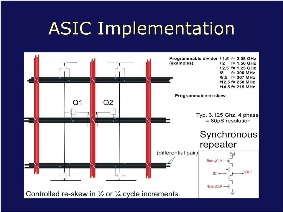
10 ASIC Implementation
11 Capacitive Loading Reduce propagation velocity Independent of parasitic capacitance Increase current in wires, but no CV 2 f power

12 Rotary Wires for ASIC Rotary distribution Synchronous components

13 Modes of Operation ASIC drive Global rotary clock to synchronize any number of: Derived clocks Other global signals Reset, Enable, Step, Scan Retain standard FFs Minimal flow impact Direct Drive Maximum power benefit. One high frequency clock grid over whole chip directly driving all FFs. Custom FFs for lowest power. Modified flow.

14 DFF Load High internal capacitance High dynamic power consumption Direct drive: Rotary clock drives Nfet and Pfet pass devices directly

15 Latch Load Less clocked C: save CV 2 f power No need to gate clock (only data)

16 Rotary Modes

17 CAD: Extraction and Simulation RLC extraction for rotary RC for data Fast SPICE for confirmation Internal STA engine

18 Physical Design Flow DESIGN ENTRY Partitioning PARTITIONING ROA SIZE PARTITIONING REGISTER INSERTION NO ROA FEASIBLE? YES CSS CLOCK SKEW SCHEDULING CSS on PARTITION I CSS on PARTITION N NO CSS on TOP BLOCK CSS FEASIBLE? YES Placement PLACEMENT REGISTER MAPPING LOGIC PLACEMENT

19 CAD: Placement & Route 1 Select rotary rings Physical implementation

20 CAD: Placement & Route 2 Clock Pin Identify communicating register-toregister paths Partitioning Static timing analysis Clock skew scheduling 28% average improvement Parallelization

21 CSS Parallelization 10k registers 25k local paths 2.5 hours 10*10 rotary clocking 150 registers 500 paths 2 secs Speed up: 44X without parallelization 1286X with parallelization Sub-optimality
22 CAD: Placement & Route 3 45 o 225 o 0 o 180 o 270 o 90 o = T/4 delay 315 o 135 o Pre-place register banks Map registers to phase Proceed with logic synthesis
23 Conclusions Look-ahead to next-generation Rotary clocking Non-zero clock skew Parallelization Implementation results to follow
24 TIMING-DRIVEN PHYSICAL DESIGN FOR DIGITAL SYNCHRONOUS VLSI CIRCUITS USING RESONANT CLOCKING QUESTIONS?
25 DESIGN AND TIMING ANALYSIS OF LEVEL-SENSITIVE DIGITAL INTEGRATED CIRCUITS BACKUP SLIDES
26 Clock Period Minimization Problem - 1 Objective function : min T Problem variables For each register R i Earliest/latest arrival times a i, A i Earliest/latest departure times d i, D i Clock signal delay t i
27 Clock Period Minimization Problem - 2 Problem Parameters For each register R i Clock-to-output delay D CQ Data-to-output D DQ Setup time S i Hold time H i For each local data path R i R j Data propagation time D P if
28 Practical Causes of Clock Skew Size Mismatches Buffer Size, Interconnect length Process Variations L eff, T ox etc. Temperature Gradients Power Supply Voltage Drop
29 Rotary Implementation Odd number of crossovers Multi-phase Relative phase information on ring Non-zero clock skew Cross-coupled inverters Low power
30 Capacitive Loading of the Rotary Ring 4.5 pf each side 0.13u x e-18 / micron [sq] = 12.7 ff on each gate Assume 10 ff on each line for wiring cap. of spur = 22.7 ff * 200 loads 4.5 pf each side
31 Benefits of Rotary Clock Architecture No practical upper frequency limitation No practical size limitation Negates the dynamic clock power Guaranteed near-zero skew Precise skew scheduling possible Negligible jitter
32 Benefits of Rotary Clock Architecture (cont d.) Largely independent of: Process variations Temperature variations Supply voltage Inherently low noise No SSN generated by clock. Differential Greater immunity to noise Less generation of noise
33 Benefits of Rotary Clock Architecture (cont d) Works for all existing IC processes Short and predictable design cycle Automated CAD tooling
Clocking. Figure by MIT OCW. 6.884 - Spring 2005 2/18/05 L06 Clocks 1
 ing Figure by MIT OCW. 6.884 - Spring 2005 2/18/05 L06 s 1 Why s and Storage Elements? Inputs Combinational Logic Outputs Want to reuse combinational logic from cycle to cycle 6.884 - Spring 2005 2/18/05
Alpha CPU and Clock Design Evolution
 Alpha CPU and Clock Design Evolution This lecture uses two papers that discuss the evolution of the Alpha CPU and clocking strategy over three CPU generations Gronowski, Paul E., et.al., High Performance
Agenda. Michele Taliercio, Il circuito Integrato, Novembre 2001
 Agenda Introduzione Il mercato Dal circuito integrato al System on a Chip (SoC) La progettazione di un SoC La tecnologia Una fabbrica di circuiti integrati 28 How to handle complexity G The engineering
How To Design A Chip Layout
 Spezielle Anwendungen des VLSI Entwurfs Applied VLSI design (IEF170) Course and contest Intermediate meeting 3 Prof. Dirk Timmermann, Claas Cornelius, Hagen Sämrow, Andreas Tockhorn, Philipp Gorski, Martin
Introduction to CMOS VLSI Design (E158) Lecture 8: Clocking of VLSI Systems
 Lecture 8: Clocking of VLSI Systems") Harris Introduction to CMOS VLSI Design (E158) Lecture 8: Clocking of VLSI Systems David Harris Harvey Mudd College [email protected] Based on EE271 developed by Mark Horowitz, Stanford University MAH
Harris Introduction to CMOS VLSI Design (E158) Lecture 8: Clocking of VLSI Systems David Harris Harvey Mudd College [email protected] Based on EE271 developed by Mark Horowitz, Stanford University MAH
Timing Methodologies (cont d) Registers. Typical timing specifications. Synchronous System Model. Short Paths. System Clock Frequency
 Registers. Typical timing specifications. Synchronous System Model. Short Paths. System Clock Frequency") Registers Timing Methodologies (cont d) Sample data using clock Hold data between clock cycles Computation (and delay) occurs between registers efinition of terms setup time: minimum time before the clocking
Registers Timing Methodologies (cont d) Sample data using clock Hold data between clock cycles Computation (and delay) occurs between registers efinition of terms setup time: minimum time before the clocking
Latch Timing Parameters. Flip-flop Timing Parameters. Typical Clock System. Clocking Overhead
 Clock - key to synchronous systems Topic 7 Clocking Strategies in VLSI Systems Peter Cheung Department of Electrical & Electronic Engineering Imperial College London Clocks help the design of FSM where
S. Venkatesh, Mrs. T. Gowri, Department of ECE, GIT, GITAM University, Vishakhapatnam, India
 Power reduction on clock-tree using Energy recovery and clock gating technique S. Venkatesh, Mrs. T. Gowri, Department of ECE, GIT, GITAM University, Vishakhapatnam, India Abstract Power consumption of
LOW POWER DESIGN OF DIGITAL SYSTEMS USING ENERGY RECOVERY CLOCKING AND CLOCK GATING
 LOW POWER DESIGN OF DIGITAL SYSTEMS USING ENERGY RECOVERY CLOCKING AND CLOCK GATING A thesis work submitted to the faculty of San Francisco State University In partial fulfillment of the requirements for
ISSCC 2003 / SESSION 13 / 40Gb/s COMMUNICATION ICS / PAPER 13.7
 ISSCC 2003 / SESSION 13 / 40Gb/s COMMUNICATION ICS / PAPER 13.7 13.7 A 40Gb/s Clock and Data Recovery Circuit in 0.18µm CMOS Technology Jri Lee, Behzad Razavi University of California, Los Angeles, CA
Power Reduction Techniques in the SoC Clock Network. Clock Power
 Power Reduction Techniques in the SoC Network Low Power Design for SoCs ASIC Tutorial SoC.1 Power Why clock power is important/large» Generally the signal with the highest frequency» Typically drives a
Lecture 7: Clocking of VLSI Systems
 Lecture 7: Clocking of VLSI Systems MAH, AEN EE271 Lecture 7 1 Overview Reading Wolf 5.3 Two-Phase Clocking (good description) W&E 5.5.1, 5.5.2, 5.5.3, 5.5.4, 5.5.9, 5.5.10 - Clocking Note: The analysis
PROGETTO DI SISTEMI ELETTRONICI DIGITALI. Digital Systems Design. Digital Circuits Advanced Topics
 PROGETTO DI SISTEMI ELETTRONICI DIGITALI Digital Systems Design Digital Circuits Advanced Topics 1 Sequential circuit and metastability 2 Sequential circuit - FSM A Sequential circuit contains: Storage
EE 459/500 HDL Based Digital Design with Programmable Logic. Lecture 16 Timing and Clock Issues
 EE 459/500 HDL Based Digital Design with Programmable Logic Lecture 16 Timing and Clock Issues 1 Overview Sequential system timing requirements Impact of clock skew on timing Impact of clock jitter on
IL2225 Physical Design
 IL2225 Physical Design Nasim Farahini [email protected] Outline Physical Implementation Styles ASIC physical design Flow Floor and Power planning Placement Clock Tree Synthesis Routing Timing Analysis Verification
NTE2053 Integrated Circuit 8 Bit MPU Compatible A/D Converter
 NTE2053 Integrated Circuit 8 Bit MPU Compatible A/D Converter Description: The NTE2053 is a CMOS 8 bit successive approximation Analog to Digital converter in a 20 Lead DIP type package which uses a differential
Topics of Chapter 5 Sequential Machines. Memory elements. Memory element terminology. Clock terminology
 Topics of Chapter 5 Sequential Machines Memory elements Memory elements. Basics of sequential machines. Clocking issues. Two-phase clocking. Testing of combinational (Chapter 4) and sequential (Chapter
A NEAR FIELD INJECTION MODEL FOR SUSCEPTIBILITY PREDICTION IN INTEGRATED CIRCUITS
 ICONIC 2007 St. Louis, MO, USA June 27-29, 2007 A NEAR FIELD INJECTION MODEL FOR SUSCEPTIBILITY PREDICTION IN INTEGRATED CIRCUITS Ali Alaeldine 12, Alexandre Boyer 3, Richard Perdriau 1, Sonia Ben Dhia
Asynchronous IC Interconnect Network Design and Implementation Using a Standard ASIC Flow
 Asynchronous IC Interconnect Network Design and Implementation Using a Standard ASIC Flow Bradley R. Quinton Dept. of Electrical and Computer Engineering University of British Columbia [email protected]
Lecture 11: Sequential Circuit Design
 Lecture 11: Sequential Circuit esign Outline Sequencing Sequencing Element esign Max and Min-elay Clock Skew Time Borrowing Two-Phase Clocking 2 Sequencing Combinational logic output depends on current
Fairchild Solutions for 133MHz Buffered Memory Modules
 AN-5009 Fairchild Semiconductor Application Note April 1999 Revised December 2000 Fairchild Solutions for 133MHz Buffered Memory Modules Fairchild Semiconductor provides several products that are compatible
Sentinel-SSO: Full DDR-Bank Power and Signal Integrity. Design Automation Conference 2014
 Sentinel-SSO: Full DDR-Bank Power and Signal Integrity Design Automation Conference 2014 1 Requirements for I/O DDR SSO Analysis Modeling Package and board I/O circuit and layout PI + SI feedback Tool
NAME AND SURNAME. TIME: 1 hour 30 minutes 1/6
 E.T.S.E.T.B. MSc in ICT FINAL EXAM VLSI Digital Design Spring Course 2005-2006 June 6, 2006 Score publication date: June 19, 2006 Exam review request deadline: June 22, 2006 Academic consultancy: June
EE 42/100 Lecture 24: Latches and Flip Flops. Rev B 4/21/2010 (2:04 PM) Prof. Ali M. Niknejad
 Prof. Ali M. Niknejad") A. M. Niknejad University of California, Berkeley EE 100 / 42 Lecture 24 p. 1/20 EE 42/100 Lecture 24: Latches and Flip Flops ELECTRONICS Rev B 4/21/2010 (2:04 PM) Prof. Ali M. Niknejad University of California,
A. M. Niknejad University of California, Berkeley EE 100 / 42 Lecture 24 p. 1/20 EE 42/100 Lecture 24: Latches and Flip Flops ELECTRONICS Rev B 4/21/2010 (2:04 PM) Prof. Ali M. Niknejad University of California,
PROGETTO DI SISTEMI ELETTRONICI DIGITALI. Digital Systems Design. Digital Circuits Advanced Topics
 PROGETTO DI SISTEMI ELETTRONICI DIGITALI Digital Systems Design Digital Circuits Advanced Topics 1 Sequential circuit and metastability 2 Sequential circuit A Sequential circuit contains: Storage elements:
Reconfigurable ECO Cells for Timing Closure and IR Drop Minimization. TingTing Hwang Tsing Hua University, Hsin-Chu
 Reconfigurable ECO Cells for Timing Closure and IR Drop Minimization TingTing Hwang Tsing Hua University, Hsin-Chu 1 Outline Introduction Engineering Change Order (ECO) Voltage drop (IR-DROP) New design
INTEGRATED CIRCUITS. For a complete data sheet, please also download:
 INTEGRATED CIRCUITS DATA SEET For a complete data sheet, please also download: The IC6 74C/CT/CU/CMOS Logic Family Specifications The IC6 74C/CT/CU/CMOS Logic Package Information The IC6 74C/CT/CU/CMOS
路 論 Chapter 15 System-Level Physical Design
 Introduction to VLSI Circuits and Systems 路 論 Chapter 15 System-Level Physical Design Dept. of Electronic Engineering National Chin-Yi University of Technology Fall 2007 Outline Clocked Flip-flops CMOS
Design Verification & Testing Design for Testability and Scan
 Overview esign for testability (FT) makes it possible to: Assure the detection of all faults in a circuit Reduce the cost and time associated with test development Reduce the execution time of performing
ICS379. Quad PLL with VCXO Quick Turn Clock. Description. Features. Block Diagram
 Quad PLL with VCXO Quick Turn Clock Description The ICS379 QTClock TM generates up to 9 high quality, high frequency clock outputs including a reference from a low frequency pullable crystal. It is designed
Architectural Level Power Consumption of Network on Chip. Presenter: YUAN Zheng
 Architectural Level Power Consumption of Network Presenter: YUAN Zheng Why Architectural Low Power Design? High-speed and large volume communication among different parts on a chip Problem: Power consumption
TRUE SINGLE PHASE CLOCKING BASED FLIP-FLOP DESIGN
 TRUE SINGLE PHASE CLOCKING BASED FLIP-FLOP DESIGN USING DIFFERENT FOUNDRIES Priyanka Sharma 1 and Rajesh Mehra 2 1 ME student, Department of E.C.E, NITTTR, Chandigarh, India 2 Associate Professor, Department
Lecture 10: Sequential Circuits
 Introduction to CMOS VLSI esign Lecture 10: Sequential Circuits avid Harris Harvey Mudd College Spring 2004 Outline q Sequencing q Sequencing Element esign q Max and Min-elay q Clock Skew q Time Borrowing
Set-Reset (SR) Latch
 Latch") et-eset () Latch Asynchronous Level sensitive cross-coupled Nor gates active high inputs (only one can be active) + + Function 0 0 0 1 0 1 eset 1 0 1 0 et 1 1 0-? 0-? Indeterminate cross-coupled Nand gates
et-eset () Latch Asynchronous Level sensitive cross-coupled Nor gates active high inputs (only one can be active) + + Function 0 0 0 1 0 1 eset 1 0 1 0 et 1 1 0-? 0-? Indeterminate cross-coupled Nand gates
DS2187 Receive Line Interface
 Receive Line Interface www.dalsemi.com FEATURES Line interface for T1 (1.544 MHz) and CEPT (2.048 MHz) primary rate networks Extracts clock and data from twisted pair or coax Meets requirements of PUB
Model-Based Synthesis of High- Speed Serial-Link Transmitter Designs
 Model-Based Synthesis of High- Speed Serial-Link Transmitter Designs Ikchan Jang 1, Soyeon Joo 1, SoYoung Kim 1, Jintae Kim 2, 1 College of Information and Communication Engineering, Sungkyunkwan University,
Lecture 10: Latch and Flip-Flop Design. Outline
 Lecture 1: Latch and Flip-Flop esign Slides orginally from: Vladimir Stojanovic Computer Systems Laboratory Stanford University [email protected] 1 Outline Recent interest in latches and flip-flops
An All-Digital Phase-Locked Loop with High Resolution for Local On-Chip Clock Synthesis
 An All-Digital Phase-Locked Loop with High Resolution for Local On-Chip Clock Synthesis Oliver Schrape 1, Frank Winkler 2, Steffen Zeidler 1, Markus Petri 1, Eckhard Grass 1, Ulrich Jagdhold 1 International
On-Chip Interconnect: The Past, Present, and Future
 On-Chip Interconnect: The Past, Present, and Future Professor Eby G. Friedman Department of Electrical and Computer Engineering University of Rochester URL: http://www.ece.rochester.edu/~friedman Future
IBIS for SSO Analysis
 IBIS for SSO Analysis Asian IBIS Summit, November 15, 2010 (Presented previously at Asian IBIS Summits, Nov. 9 & 12, 2010) Haisan Wang Joshua Luo Jack Lin Zhangmin Zhong Contents Traditional I/O SSO Analysis
Low Power AMD Athlon 64 and AMD Opteron Processors
 Low Power AMD Athlon 64 and AMD Opteron Processors Hot Chips 2004 Presenter: Marius Evers Block Diagram of AMD Athlon 64 and AMD Opteron Based on AMD s 8 th generation architecture AMD Athlon 64 and AMD
Sequential 4-bit Adder Design Report
 UNIVERSITY OF WATERLOO Faculty of Engineering E&CE 438: Digital Integrated Circuits Sequential 4-bit Adder Design Report Prepared by: Ian Hung (ixxxxxx), 99XXXXXX Annette Lo (axxxxxx), 99XXXXXX Pamela
AVX EMI SOLUTIONS Ron Demcko, Fellow of AVX Corporation Chris Mello, Principal Engineer, AVX Corporation Brian Ward, Business Manager, AVX Corporation
 AVX EMI SOLUTIONS Ron Demcko, Fellow of AVX Corporation Chris Mello, Principal Engineer, AVX Corporation Brian Ward, Business Manager, AVX Corporation Abstract EMC compatibility is becoming a key design
Introduction to Digital System Design
 Introduction to Digital System Design Chapter 1 1 Outline 1. Why Digital? 2. Device Technologies 3. System Representation 4. Abstraction 5. Development Tasks 6. Development Flow Chapter 1 2 1. Why Digital
TIMING ISSUES IN DIGITAL CIRCUITS
 chapter10_141.fm Page 42 Tuesday, April 16, 2002 9:12 AM CHAPTER 10 TIMING ISSUES IN DIGITAL CIRCUITS Impact of clock skew and jitter on performance and functionality n Alternative timing methodologies
University of Texas at Dallas. Department of Electrical Engineering. EEDG 6306 - Application Specific Integrated Circuit Design
 University of Texas at Dallas Department of Electrical Engineering EEDG 6306 - Application Specific Integrated Circuit Design Synopsys Tools Tutorial By Zhaori Bi Minghua Li Fall 2014 Table of Contents
Class 11: Transmission Gates, Latches
 Topics: 1. Intro 2. Transmission Gate Logic Design 3. X-Gate 2-to-1 MUX 4. X-Gate XOR 5. X-Gate 8-to-1 MUX 6. X-Gate Logic Latch 7. Voltage Drop of n-ch X-Gates 8. n-ch Pass Transistors vs. CMOS X-Gates
ECE124 Digital Circuits and Systems Page 1
 ECE124 Digital Circuits and Systems Page 1 Chip level timing Have discussed some issues related to timing analysis. Talked briefly about longest combinational path for a combinational circuit. Talked briefly
PowerPC Microprocessor Clock Modes
 nc. Freescale Semiconductor AN1269 (Freescale Order Number) 1/96 Application Note PowerPC Microprocessor Clock Modes The PowerPC microprocessors offer customers numerous clocking options. An internal phase-lock
Application Note 58 Crystal Considerations with Dallas Real Time Clocks
 www.dalsemi.com Application Note 58 Crystal Considerations with Dallas Real Time Clocks Dallas Semiconductor offers a variety of real time clocks (RTCs). The majority of these are available either as integrated
11. High-Speed Differential Interfaces in Cyclone II Devices
 11. High-Speed Differential Interfaces in Cyclone II Devices CII51011-2.2 Introduction From high-speed backplane applications to high-end switch boxes, low-voltage differential signaling (LVDS) is the
CMOS, the Ideal Logic Family
 CMOS, the Ideal Logic Family INTRODUCTION Let s talk about the characteristics of an ideal logic family. It should dissipate no power, have zero propagation delay, controlled rise and fall times, and have
Lecture 11. Clocking High-Performance Microprocessors
 Lecture 11 Clocking High-Performance Microprocessors Computer Systems Laboratory Stanford University [email protected] Copyright 2007 Ron Ho, Mark Horowitz 1 Overview Readings (Actually for today s
Efficient Interconnect Design with Novel Repeater Insertion for Low Power Applications
 Efficient Interconnect Design with Novel Repeater Insertion for Low Power Applications TRIPTI SHARMA, K. G. SHARMA, B. P. SINGH, NEHA ARORA Electronics & Communication Department MITS Deemed University,
MADR-009443-0001TR. Quad Driver for GaAs FET or PIN Diode Switches and Attenuators. Functional Schematic. Features. Description. Pin Configuration 2
 Features Functional Schematic High Voltage CMOS Technology Four Channel Positive Voltage Control CMOS device using TTL input levels Low Power Dissipation Low Cost 4x4 mm, 20-lead PQFN Package 100% Matte
Hunting Asynchronous CDC Violations in the Wild
 Hunting Asynchronous Violations in the Wild Chris Kwok Principal Engineer May 4, 2015 is the #2 Verification Problem Why is a Big Problem: 10 or More Clock Domains are Common Even FPGA Users Are Suffering
Harmonics and Noise in Photovoltaic (PV) Inverter and the Mitigation Strategies
 Inverter and the Mitigation Strategies") Soonwook Hong, Ph. D. Michael Zuercher Martinson Harmonics and Noise in Photovoltaic (PV) Inverter and the Mitigation Strategies 1. Introduction PV inverters use semiconductor devices to transform the
Soonwook Hong, Ph. D. Michael Zuercher Martinson Harmonics and Noise in Photovoltaic (PV) Inverter and the Mitigation Strategies 1. Introduction PV inverters use semiconductor devices to transform the
Layout of Multiple Cells
 Layout of Multiple Cells Beyond the primitive tier primitives add instances of primitives add additional transistors if necessary add substrate/well contacts (plugs) add additional polygons where needed
1. Description. 2. Feature. 3. PIN Configuration
 1. Description is a 9-channel LED driver control IC. Internal integrated with MCU digital interface, data flip-latch, LED high voltage driver and so on.through the external MCU control, the chip can achieve
A 1.62/2.7/5.4 Gbps Clock and Data Recovery Circuit for DisplayPort 1.2 with a single VCO
 JOURNAL OF SEMICONDUCTOR TECHNOLOGY AND SCIENCE, VOL.13, NO.3, JUNE, 2013 http://dx.doi.org/10.5573/jsts.2013.13.3.185 A 1.62/2.7/5.4 Clock and Data Recovery Circuit for DisplayPort 1.2 with a single VCO
Phase-Locked Loop Based Clock Generators
 Phase-Locked Loop Based Clock Generators INTRODUCTION As system clock frequencies reach 100 MHz and beyond maintaining control over clock becomes very important In addition to generating the various clocks
DATA SHEET. HEF40193B MSI 4-bit up/down binary counter. For a complete data sheet, please also download: INTEGRATED CIRCUITS
 INTEGRATED CIRCUITS DATA SHEET For a complete data sheet, please also download: The IC04 LOCMOS HE4000B Logic Family Specifications HEF, HEC The IC04 LOCMOS HE4000B Logic Package Outlines/Information HEF,
Abstract. Cycle Domain Simulator for Phase-Locked Loops
 Abstract Cycle Domain Simulator for Phase-Locked Loops Norman James December 1999 As computers become faster and more complex, clock synthesis becomes critical. Due to the relatively slower bus clocks
Programmable Single-/Dual-/Triple- Tone Gong SAE 800
 Programmable Single-/Dual-/Triple- Tone Gong Preliminary Data SAE 800 Bipolar IC Features Supply voltage range 2.8 V to 18 V Few external components (no electrolytic capacitor) 1 tone, 2 tones, 3 tones
Signal Types and Terminations
 Helping Customers Innovate, Improve & Grow Application Note Signal Types and Terminations Introduction., H, LV, Sinewave, Clipped Sinewave, TTL, PECL,,, CML Oscillators and frequency control devices come
Clock Distribution Networks in Synchronous Digital Integrated Circuits
 Clock Distribution Networks in Synchronous Digital Integrated Circuits EBY G. FRIEDMAN Invited Paper Clock distribution networks synchronize the flow of data signals among synchronous data paths. The design
DESIGN CHALLENGES OF TECHNOLOGY SCALING
 DESIGN CHALLENGES OF TECHNOLOGY SCALING IS PROCESS TECHNOLOGY MEETING THE GOALS PREDICTED BY SCALING THEORY? AN ANALYSIS OF MICROPROCESSOR PERFORMANCE, TRANSISTOR DENSITY, AND POWER TRENDS THROUGH SUCCESSIVE
Contents. Preface. xiii. Part I 1
 Contents Preface xiii Part I 1 Chapter 1 Introduction to Frequency-Modulated Continuous-Wave 3 Radar 1.1 Brief History 3 1.2 Examples of Use of FMCW Radar 5 1.2.1 Radio Altimeters 5 1.2.2 Level-Measuring
Sequential Logic. (Materials taken from: Principles of Computer Hardware by Alan Clements )
") Sequential Logic (Materials taken from: Principles of Computer Hardware by Alan Clements ) Sequential vs. Combinational Circuits Combinatorial circuits: their outputs are computed entirely from their present
Sequential Logic (Materials taken from: Principles of Computer Hardware by Alan Clements ) Sequential vs. Combinational Circuits Combinatorial circuits: their outputs are computed entirely from their present
MM74C150 MM82C19 16-Line to 1-Line Multiplexer 3-STATE 16-Line to 1-Line Multiplexer
 MM74C150 MM82C19 16-Line to 1-Line Multiplexer 3-STATE 16-Line to 1-Line Multiplexer General Description The MM74C150 and MM82C19 multiplex 16 digital lines to 1 output. A 4-bit address code determines
Spread-Spectrum Crystal Multiplier DS1080L. Features
 Rev 1; 3/0 Spread-Spectrum Crystal Multiplier General Description The is a low-jitter, crystal-based clock generator with an integrated phase-locked loop (PLL) to generate spread-spectrum clock outputs
Gate Delay Model. Estimating Delays. Effort Delay. Gate Delay. Computing Logical Effort. Logical Effort
 Estimating Delays Would be nice to have a back of the envelope method for sizing gates for speed Logical Effort Book by Sutherland, Sproull, Harris Chapter 1 is on our web page Also Chapter 4 in our textbook
International Journal of Electronics and Computer Science Engineering 1482
 International Journal of Electronics and Computer Science Engineering 1482 Available Online at www.ijecse.org ISSN- 2277-1956 Behavioral Analysis of Different ALU Architectures G.V.V.S.R.Krishna Assistant
ATE-A1 Testing Without Relays - Using Inductors to Compensate for Parasitic Capacitance
 Introduction (Why Get Rid of Relays?) Due to their size, cost and relatively slow (millisecond) operating speeds, minimizing the number of mechanical relays is a significant goal of any ATE design. This
ISSCC 2003 / SESSION 4 / CLOCK RECOVERY AND BACKPLANE TRANSCEIVERS / PAPER 4.7
 ISSCC 2003 / SESSION 4 / CLOCK RECOVERY AND BACKPLANE TRANSCEIVERS / PAPER 4.7 4.7 A 2.7 Gb/s CDMA-Interconnect Transceiver Chip Set with Multi-Level Signal Data Recovery for Re-configurable VLSI Systems
ASYNCHRONOUS COUNTERS
 LB no.. SYNCHONOUS COUNTES. Introduction Counters are sequential logic circuits that counts the pulses applied at their clock input. They usually have 4 bits, delivering at the outputs the corresponding
Class 18: Memories-DRAMs
 Topics: 1. Introduction 2. Advantages and Disadvantages of DRAMs 3. Evolution of DRAMs 4. Evolution of DRAMs 5. Basics of DRAMs 6. Basics of DRAMs 7. Write Operation 8. SA-Normal Operation 9. SA-Read Operation
On-chip clock error characterization for clock distribution system
 On-chip clock error characterization for clock distribution system Chuan Shan, Dimitri Galayko, François Anceau Laboratoire d informatique de Paris 6 (LIP6) Université Pierre & Marie Curie (UPMC), Paris,
Figure 1 FPGA Growth and Usage Trends
 White Paper Avoiding PCB Design Mistakes in FPGA-Based Systems System design using FPGAs is significantly different from the regular ASIC and processor based system design. In this white paper, we will
ZL40221 Precision 2:6 LVDS Fanout Buffer with Glitchfree Input Reference Switching and On-Chip Input Termination Data Sheet
 Features Inputs/Outputs Accepts two differential or single-ended inputs LVPECL, LVDS, CML, HCSL, LVCMOS Glitch-free switching of references On-chip input termination and biasing for AC coupled inputs Six
SPREAD SPECTRUM CLOCK GENERATOR. Features
 DATASHEET ICS7152 Description The ICS7152-01, -02, -11, and -12 are clock generators for EMI (Electro Magnetic Interference) reduction (see below for frequency ranges and multiplier ratios). Spectral peaks
3-Phase DC Brushless Motor Pre-Drivers Technical Information NJM2625A
 3Phase DC Brushless Motor PreDrivers 1.FEATURE NJM2625 is a controller and predriver for speed control 3phase blushless DC motor. The device provides the proper sequencing of 3phase drive output with external
Asynchronous counters, except for the first block, work independently from a system clock.
 Counters Some digital circuits are designed for the purpose of counting and this is when counters become useful. Counters are made with flip-flops, they can be asynchronous or synchronous and they can
Chapter 13: Verification
 Chapter 13: Verification Prof. Ming-Bo Lin Department of Electronic Engineering National Taiwan University of Science and Technology Digital System Designs and Practices Using Verilog HDL and FPGAs @ 2008-2010,
A 3.2Gb/s Clock and Data Recovery Circuit Without Reference Clock for a High-Speed Serial Data Link
 A 3.2Gb/s Clock and Data Recovery Circuit Without Reference Clock for a High-Speed Serial Data Link Kang jik Kim, Ki sang Jeong, Seong ik Cho The Department of Electronics Engineering Chonbuk National
INTEGRATED CIRCUITS. For a complete data sheet, please also download:
 INTEGRATED CIRCUITS DATA SEET For a complete data sheet, please also download: The IC6 74C/CT/CU/CMOS ogic Family Specifications The IC6 74C/CT/CU/CMOS ogic Package Information The IC6 74C/CT/CU/CMOS ogic
CERAMIC RESONATOR PRINCIPLES
 CERAMIC RESONATOR PRINCIPLES Principles of Operation for Ceramic Resonators Equivalent Circuit Constants: Fig.1.2 shows the symbol for a ceramic resonator. The impedance and phase characteristics measured
SECTION 2 Transmission Line Theory
 SEMICONDUCTOR DESIGN GUIDE Transmission Line Theory SECTION 2 Transmission Line Theory Introduction The ECLinPS family has pushed the world of ECL into the realm of picoseconds. When output transitions
Curriculum for a Master s Degree in ECE with focus on Mixed Signal SOC Design
 Curriculum for a Master s Degree in ECE with focus on Mixed Signal SOC Design Department of Electrical and Computer Engineering Overview The VLSI Design program is part of two tracks in the department:
Application Note 58 Crystal Considerations for Dallas Real-Time Clocks
 www.maxim-ic.com Application Note 58 Crystal Considerations for Dallas Real-Time Clocks OVERVIEW This application note describes crystal selection and layout techniques for connecting a 32,768Hz crystal
Application Note: PCB Design By: Wei-Lung Ho
 Application Note: PCB Design By: Wei-Lung Ho Introduction: A printed circuit board (PCB) electrically connects circuit components by routing conductive traces to conductive pads designed for specific components
DP8570A DP8570A Timer Clock Peripheral (TCP)
") DP8570A DP8570A Timer Clock Peripheral (TCP) Literature Number: SNAS557 DP8570A Timer Clock Peripheral (TCP) General Description The DP8570A is intended for use in microprocessor based systems where information
DP8570A DP8570A Timer Clock Peripheral (TCP) Literature Number: SNAS557 DP8570A Timer Clock Peripheral (TCP) General Description The DP8570A is intended for use in microprocessor based systems where information
Design and Applications of HCPL-3020 and HCPL-0302 Gate Drive Optocouplers
 Design and Applications of HCPL-00 and HCPL-00 Gate Drive Optocouplers Application Note 00 Introduction The HCPL-00 (DIP-) and HCPL-00 (SO-) consist of GaAsP LED optically coupled to an integrated circuit
Status of the design of the TDC for the GTK TDCpix ASIC
 Status of the design of the TDC for the GTK TDCpix ASIC Gianluca Aglieri Rinella, Lukas Perktold DLL design review meeting, 16 03 2011 Outline Introduction Purpose and objectives Reminder Challenges of
. MEDIUM SPEED OPERATION - 8MHz (typ.) @ . MULTI-PACKAGE PARALLEL CLOCKING FOR HCC4029B HCF4029B PRESETTABLE UP/DOWN COUNTER BINARY OR BCD DECADE
 @ . MULTI-PACKAGE PARALLEL CLOCKING FOR HCC4029B HCF4029B PRESETTABLE UP/DOWN COUNTER BINARY OR BCD DECADE") HCC4029B HCF4029B PRESETTABLE UP/DOWN COUNTER BINARY OR BCD DECADE. MEDIUM SPEED OPERATION - 8MHz (typ.) @ CL = 50pF AND DD-SS = 10. MULTI-PACKAGE PARALLEL CLOCKING FOR SYNCHRONOUS HIGH SPEED OUTPUT RES-
HCC4029B HCF4029B PRESETTABLE UP/DOWN COUNTER BINARY OR BCD DECADE. MEDIUM SPEED OPERATION - 8MHz (typ.) @ CL = 50pF AND DD-SS = 10. MULTI-PACKAGE PARALLEL CLOCKING FOR SYNCHRONOUS HIGH SPEED OUTPUT RES-