McPAT: An Integrated Power, Area, and Timing Modeling Framework for Multicore and Manycore Architectures
|
|
|
- Lily Holland
- 9 years ago
- Views:
Transcription
1 McPAT: An Integrated Power, Area, and Timing Modeling Framework for Multicore and Manycore Architectures Sheng Li, Junh Ho Ahn, Richard Strong, Jay B. Brockman, Dean M Tullsen, Norman Jouppi MICRO 2009

2 How do u estimate access time? How do u estimate power? How do you estimate area? CACTI started in 1994 from the following papers. Only area and time initially. Power added later.

3 How do u estimate access time?

4 What type of models are these? Are they accurate? How could you estimate more accurately? SPICE

5 Power Estimation Circuit Level Power Estimation using SPICE Gate level power estimation The first such tool integrated with Synopsis around 1995 (Power Mill) Low Power libraries provided along with high speed libraries for use in synthesis Synopsis, Cadence, Magma all have builtin power estimation now Power management primitives are being incorporated into HDL level design

6 Motivation Tools both limit and drive research directions New demands Multicore/manycore Evaluate power, timing and area Different source of power dissipation Deep-submicron

7 Related Work Wattch: Enabling a tremendous surge in power-related research Orion: Combined Wattch s core power model with a router power model CACTI: First tool in rapid power, area, and timing estimation

8 How did Wattch work?

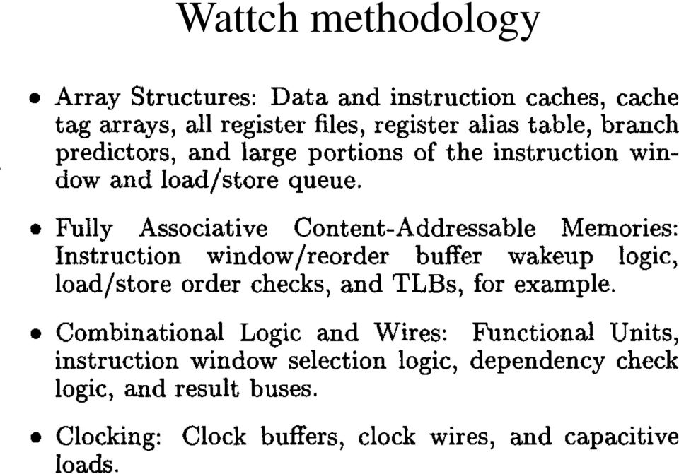
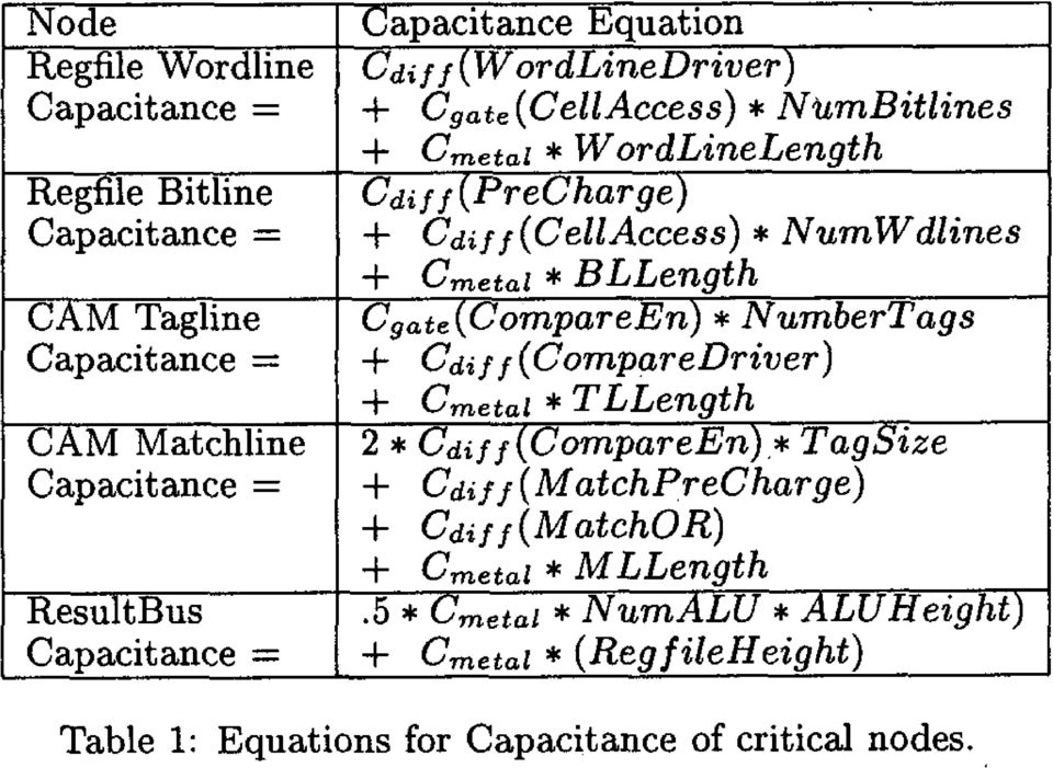
9 Wattch methodology
10
11

12 What s wrong with previous work? Wattch No timing and area models Only models dynamic power consumption Use simple linear scaling model RUU model from Simplescalar Orion2 No short circuit power or timing Incomplete CACTI

13 Contributions First integrated power, area, and timing modeling framework Model all three types of power dissipation Complete, integrated solution for multithreaded and multicore processor power Deep-submicron tech. that no longer linear


14 Overview
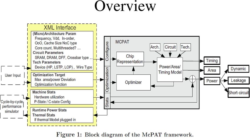
15 Integrated Approach Power Dynamic: Similar to Wattch Short Circuit: IEEE TCAD 00 Leakage: MASTAR & Intel Timing CACTI with extension Area CACTI Empirical modeling for complex logic

16 Hierarchical Approach
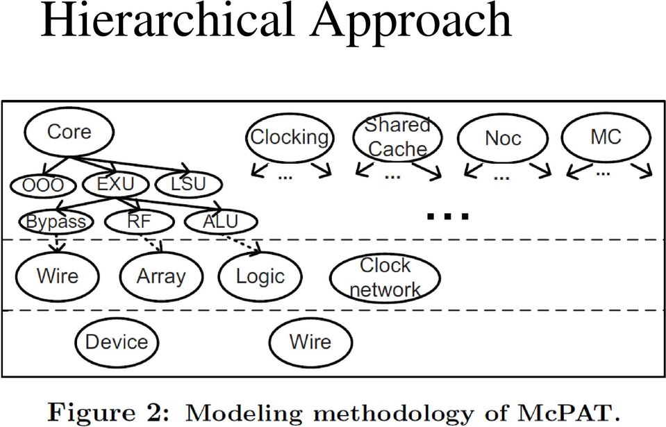
17 Architecture Level Core Divided into several main units: e.g. IFU, EXU, LSU, OOO issue/dispatch unit NoC On-Chip Caches Memory Controller Clocking Signal links and routers Coherent cache 3 main hardware structure Empirical model for physical interface (PHY) PLL and clock distribution network Empirical model for PLL power
 PLL and clock distribution network")
18 Circuit Level Short wires as one-section Pi-RC model Wires Long wires as a buffered wire model Arrays Logic Clock Distribution Network Based on CACTI with extensions Highly regular: CACTI Less regular: Model from Intel, AMD and Sun Highly customized: Empirical, from Intel and Sun Separate circuit model Global, Domain, and Local


19 Validation
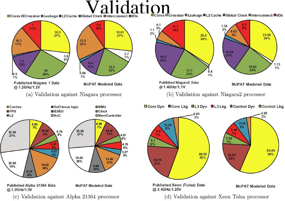

20 Validation Average error 1 st Contributor Error / % in total pwr Niagara 1.47W / 23% 74% / 1% Niagara2 1.87W / 26% 47% / 5% Alpha W / 26% 45% / 3% Xeon Tulsa 4.2W / 17% 29% / 3%

21 Scaling & Clustering New generation: Double # of cores Keep the same micro-architecture

22 Parameters and Benchmarks
23 Area and Power

24 Performance and Efficiency

25 Performance and Efficiency
26 In-order vs. OOO with M5
27 Figure of Merit Metrics 1. EDA^2 2. EDA 3. ED 4. ED^2 5. AT 6. AT^2
28 Power and Energy Power is drawn from a voltage source attached to the V DD pin(s) of a chip. Instantaneous Power: P( t) i ( t) V DD DD Energy: Average Power: T E P( t) dt i ( t) V dt T DD DD E 1 Pavg idd() t VDDdt T T T
29 Power Dissipation in CMOS ICs There are 4 sources of power dissipation in digital ICs Pavg = Pswitching + Pshortcircuit + Pleakage + Pstatic Pavg = Time Averaged Power Pswitching = Switching Component of Power Pshortcircuit = Short Circuit Component of Power Pleakage = Leakage Component of Power Pstatic = Static Component of Power
30 Dynamic Power Dissipation Caused by the switching of the circuits (Pswitching + Pshortcircuit) Higher operating frequency -> more frequent switching activities and results in increased power dissipation
31 Switching Power Dissipation Vdd Vin Vout CL Energy/transition = C L * V dd 2 Power = Energy/transition * f = C L * V dd 2 * f * a Switching power is required to charge and discharge load capacitances when transistors switch., CL = Load Capacitance f = Clock Frequency a = Activity Factor
32 Short Circuit Current When transistors switch, both nmos and pmos networks may be momentarily ON at once Leads to a blip of short circuit current. < 10% of dynamic power if rise/fall times are comparable for input and output
33 Short Circuit Current Vdd Vin Vout C L 0.15 I VDD (ma) V in (V)
34 Power Dissipation in CMOS ICs Pavg = Pswitching + Pshortcircuit + Pleakage + Pstatic = a CL V VDD f + ISC VDD + Ileakage VDD + Istatic VDD CL = Load Capacitance V = Voltage Swing (most cases V = VDD) f = Clock Frequency ISC = Short circuit current Ileakage = Leakage Current Istatic = Static Current a = Activity Factor
35 Leakage Power The power that is dissipated from the devices, when they are in idle state. Adds to average power, not peak power More expensive than dynamic power Independent of transistor utilization
36 CMOS Leakage Current (a) (b) (c) (a) NMOS-transistor (b) Ideal switch (c) leaking device Any guesses on what percent of chip power is leakage power nowadays?
37 Leakage Power Trends Source: ITRS
38 Leakage Power Trends in Nanoscale Source: Intel
39 Transistor Leakage Current Mechanisms There are 6 different leakage current mechanisms in CMOS devices: Subthreshold leakage current (I sub ) Weak inversion conduction current Gate Oxide Tunneling Current (I gate ) Tunneling of electrons from substrate to gate Reverse Biased PN Junction Leakage Current (I rev ) Current flows into the well from the drain and source Gate Induced Drain Leakage Current (I gidl ) Due to high field effect in the drain junction Hot Carrier Gate Leakage Current (I hot ) Due to high electric field near the Si-SiO 2 Punch Through Leakage Current (I PT ) Proximity of the drain and source Subthreshold leakage current and Gate Oxide Tunneling Current are the most significant ones
40 Subthreshold Leakage Current Even though the transistor is logically turned OFF, there is a non-zero leakage current through the channel. This current is known as the subthreshold leakage current because it occurs when the gate voltage is below its threshold voltage

41 What Affects Leakage Power?
42 Static Current Static CMOS circuits are not supposed to consume constant static power from constant static current flow Sometimes designers deviate from CMOS design style Pseudo NMOS circuits This is an example where power is traded for area efficiency. The pseudo NMOS circuit does not require a P-transistor network and saves half the transistors required for logic computation, as compared to CMOS logic If an output signal is known to have a very high probability of logic 1 (say 0.99), it may make sense to implement the computation in pseudo NMOS logic
43 Static Current (contd..) The circuit has a special property: The static current flows only when the output is at logic 0 Make use of this property in low power design In general, the pseudo NMOS circuit is not used on random logic For special circuits such as PLAs or register files it is useful due to its efficient area usage In such as circuit there is a constant current flow from Vdd to Vss
44 Power Dissipation in CMOS ICs Pavg = Pswitching + Pshortcircuit + Pleakage + Pstatic = a CL V VDD f + ISC VDD + Ileakage VDD + Istatic VDD CL = Load Capacitance V = Voltage Swing (most cases V = VDD) f = Clock Frequency ISC = Short circuit current Ileakage = Leakage Current Istatic = Static Current a = Activity Factor
45 Basic Principles of Low Power Design Power reduction can be achieved at most design abstraction levels: Material Process technology Physical Design (Floor Plan, placement & routing) Circuit design techniques Transistor sizing Logic restructuring Architecture transformation Alternative computation algorithm
46 Basic Principles of Low Power Design Reduce Voltage Reduce Frequency Reduce Capacitance Reduce activity factor Use of different number representation, counting sequence etc. Alternate logic implementation Reduce Static components of power Transistor Sizing Layout Techniques Careful circuit design
47 Popular Techniques in Power Aware Design DVFS (Dynamic Voltage and Frequency Scaling) Low Power Modes Power Gating Clock Gating Logic Restructuring Compiler Control of Power Operating System Management of Power
48 Power Estimation Circuit Level Power Estimation using SPICE Gate level power estimation The first such tool integrated with Synopsis around 1995 (Power Mill) Low Power libraries provided along with high speed libraries for use in synthesis Synopsis, Cadence, Magma all have builtin power estimation now Power management primitives are being incorporated into HDL level design
Low Power AMD Athlon 64 and AMD Opteron Processors
 Low Power AMD Athlon 64 and AMD Opteron Processors Hot Chips 2004 Presenter: Marius Evers Block Diagram of AMD Athlon 64 and AMD Opteron Based on AMD s 8 th generation architecture AMD Athlon 64 and AMD
System on Chip Design. Michael Nydegger
 Short Questions, 26. February 2015 What is meant by the term n-well process? What does this mean for the n-type MOSFETs in your design? What is the meaning of the threshold voltage (practically)? What
DESIGN CHALLENGES OF TECHNOLOGY SCALING
 DESIGN CHALLENGES OF TECHNOLOGY SCALING IS PROCESS TECHNOLOGY MEETING THE GOALS PREDICTED BY SCALING THEORY? AN ANALYSIS OF MICROPROCESSOR PERFORMANCE, TRANSISTOR DENSITY, AND POWER TRENDS THROUGH SUCCESSIVE
Design and analysis of flip flops for low power clocking system
 Design and analysis of flip flops for low power clocking system Gabariyala sabadini.c PG Scholar, VLSI design, Department of ECE,PSNA college of Engg and Tech, Dindigul,India. Jeya priyanka.p PG Scholar,
Class 11: Transmission Gates, Latches
 Topics: 1. Intro 2. Transmission Gate Logic Design 3. X-Gate 2-to-1 MUX 4. X-Gate XOR 5. X-Gate 8-to-1 MUX 6. X-Gate Logic Latch 7. Voltage Drop of n-ch X-Gates 8. n-ch Pass Transistors vs. CMOS X-Gates
International Journal of Electronics and Computer Science Engineering 1482
 International Journal of Electronics and Computer Science Engineering 1482 Available Online at www.ijecse.org ISSN- 2277-1956 Behavioral Analysis of Different ALU Architectures G.V.V.S.R.Krishna Assistant
Here we introduced (1) basic circuit for logic and (2)recent nano-devices, and presented (3) some practical issues on nano-devices.
 basic circuit for logic and (2)recent nano-devices, and presented (3) some practical issues on nano-devices.") Outline Here we introduced () basic circuit for logic and (2)recent nano-devices, and presented (3) some practical issues on nano-devices. Circuit Logic Gate A logic gate is an elemantary building block
Outline Here we introduced () basic circuit for logic and (2)recent nano-devices, and presented (3) some practical issues on nano-devices. Circuit Logic Gate A logic gate is an elemantary building block
路 論 Chapter 15 System-Level Physical Design
 Introduction to VLSI Circuits and Systems 路 論 Chapter 15 System-Level Physical Design Dept. of Electronic Engineering National Chin-Yi University of Technology Fall 2007 Outline Clocked Flip-flops CMOS
Fault Modeling. Why model faults? Some real defects in VLSI and PCB Common fault models Stuck-at faults. Transistor faults Summary
 Fault Modeling Why model faults? Some real defects in VLSI and PCB Common fault models Stuck-at faults Single stuck-at faults Fault equivalence Fault dominance and checkpoint theorem Classes of stuck-at
1. Memory technology & Hierarchy
 1. Memory technology & Hierarchy RAM types Advances in Computer Architecture Andy D. Pimentel Memory wall Memory wall = divergence between CPU and RAM speed We can increase bandwidth by introducing concurrency
Agenda. Michele Taliercio, Il circuito Integrato, Novembre 2001
 Agenda Introduzione Il mercato Dal circuito integrato al System on a Chip (SoC) La progettazione di un SoC La tecnologia Una fabbrica di circuiti integrati 28 How to handle complexity G The engineering
Low leakage and high speed BCD adder using clock gating technique
 Low leakage and high speed BCD adder using clock gating technique Mr. Suri shiva 1 Mr K.R.Anudeep Laxmikanth 2 Mr. Naveen Kumar.Ch 3 Abstract The growing market of mobile, battery powered electronic systems
CO2005: Electronics I (FET) Electronics I, Neamen 3th Ed. 1
 Electronics I, Neamen 3th Ed. 1") CO2005: Electronics I The Field-Effect Transistor (FET) Electronics I, Neamen 3th Ed. 1 MOSFET The metal-oxide-semiconductor field-effect transistor (MOSFET) becomes a practical reality in the 1970s. The
CO2005: Electronics I The Field-Effect Transistor (FET) Electronics I, Neamen 3th Ed. 1 MOSFET The metal-oxide-semiconductor field-effect transistor (MOSFET) becomes a practical reality in the 1970s. The
Power Reduction Techniques in the SoC Clock Network. Clock Power
 Power Reduction Techniques in the SoC Network Low Power Design for SoCs ASIC Tutorial SoC.1 Power Why clock power is important/large» Generally the signal with the highest frequency» Typically drives a
Reconfigurable ECO Cells for Timing Closure and IR Drop Minimization. TingTing Hwang Tsing Hua University, Hsin-Chu
 Reconfigurable ECO Cells for Timing Closure and IR Drop Minimization TingTing Hwang Tsing Hua University, Hsin-Chu 1 Outline Introduction Engineering Change Order (ECO) Voltage drop (IR-DROP) New design
Alpha CPU and Clock Design Evolution
 Alpha CPU and Clock Design Evolution This lecture uses two papers that discuss the evolution of the Alpha CPU and clocking strategy over three CPU generations Gronowski, Paul E., et.al., High Performance
Integrated Circuits & Systems
 Federal University of Santa Catarina Center for Technology Computer Science & Electronics Engineering Integrated Circuits & Systems INE 5442 Lecture 11 MOSFET part 2 [email protected] I D -V DS Characteristics
Leakage Power Reduction Using Sleepy Stack Power Gating Technique
 Leakage Power Reduction Using Sleepy Stack Power Gating Technique M.Lavanya, P.Anitha M.E Student [Applied Electronics], Dept. of ECE, Kingston Engineering College, Vellore, Tamil Nadu, India Assistant
VLSI Design Verification and Testing
 VLSI Design Verification and Testing Instructor Chintan Patel (Contact using email: [email protected]). Text Michael L. Bushnell and Vishwani D. Agrawal, Essentials of Electronic Testing, for Digital,
Testing Low Power Designs with Power-Aware Test Manage Manufacturing Test Power Issues with DFTMAX and TetraMAX
 White Paper Testing Low Power Designs with Power-Aware Test Manage Manufacturing Test Power Issues with DFTMAX and TetraMAX April 2010 Cy Hay Product Manager, Synopsys Introduction The most important trend
TRUE SINGLE PHASE CLOCKING BASED FLIP-FLOP DESIGN
 TRUE SINGLE PHASE CLOCKING BASED FLIP-FLOP DESIGN USING DIFFERENT FOUNDRIES Priyanka Sharma 1 and Rajesh Mehra 2 1 ME student, Department of E.C.E, NITTTR, Chandigarh, India 2 Associate Professor, Department
A Taxonomy and Survey of Energy-Efficient Data Centers and Cloud Computing Systems
 A Taxonomy and Survey of Energy-Efficient Data Centers and Cloud Computing Systems Anton Beloglazov, Rajkumar Buyya, Young Choon Lee, and Albert Zomaya Present by Leping Wang 1/25/2012 Outline Background
Introduction to CMOS VLSI Design
 Introduction to CMOS VLSI esign Slides adapted from: N. Weste,. Harris, CMOS VLSI esign, Addison-Wesley, 3/e, 24 Introduction Integrated Circuits: many transistors on one chip Very Large Scale Integration
How To Design A Chip Layout
 Spezielle Anwendungen des VLSI Entwurfs Applied VLSI design (IEF170) Course and contest Intermediate meeting 3 Prof. Dirk Timmermann, Claas Cornelius, Hagen Sämrow, Andreas Tockhorn, Philipp Gorski, Martin
Chapter 10 Advanced CMOS Circuits
 Transmission Gates Chapter 10 Advanced CMOS Circuits NMOS Transmission Gate The active pull-up inverter circuit leads one to thinking about alternate uses of NMOS devices. Consider the circuit shown in
Introduction to VLSI Programming. TU/e course 2IN30. Prof.dr.ir. Kees van Berkel Dr. Johan Lukkien [Dr.ir. Ad Peeters, Philips Nat.
 Introduction to VLSI Programming TU/e course 2IN30 Prof.dr.ir. Kees van Berkel Dr. Johan Lukkien [Dr.ir. Ad Peeters, Philips Nat.Lab] Introduction to VLSI Programming Goals Create silicon (CMOS) awareness
Three-Phase Dual-Rail Pre-Charge Logic
 Infineon Page 1 CHES 2006 - Yokohama Three-Phase Dual-Rail Pre-Charge Logic L. Giancane, R. Luzzi, A. Trifiletti {marco.bucci, raimondo.luzzi}@infineon.com {giancane, trifiletti}@die.mail.uniroma1.it Summary
Implementation Details
 LEON3-FT Processor System Scan-I/F FT FT Add-on Add-on 2 2 kbyte kbyte I- I- Cache Cache Scan Scan Test Test UART UART 0 0 UART UART 1 1 Serial 0 Serial 1 EJTAG LEON_3FT LEON_3FT Core Core 8 Reg. Windows
CMOS Power Consumption and C pd Calculation
 CMOS Power Consumption and C pd Calculation SCAA035B June 1997 1 IMPORTANT NOTICE Texas Instruments (TI) reserves the right to make changes to its products or to discontinue any semiconductor product or
Efficient Interconnect Design with Novel Repeater Insertion for Low Power Applications
 Efficient Interconnect Design with Novel Repeater Insertion for Low Power Applications TRIPTI SHARMA, K. G. SHARMA, B. P. SINGH, NEHA ARORA Electronics & Communication Department MITS Deemed University,
CMOS, the Ideal Logic Family
 CMOS, the Ideal Logic Family INTRODUCTION Let s talk about the characteristics of an ideal logic family. It should dissipate no power, have zero propagation delay, controlled rise and fall times, and have
ARM Cortex-A9 MPCore Multicore Processor Hierarchical Implementation with IC Compiler
 ARM Cortex-A9 MPCore Multicore Processor Hierarchical Implementation with IC Compiler DAC 2008 Philip Watson Philip Watson Implementation Environment Program Manager ARM Ltd Background - Who Are We? Processor
CD4027BMS. CMOS Dual J-K Master-Slave Flip-Flop. Pinout. Features. Functional Diagram. Applications. Description. December 1992
 CD7BMS December 199 CMOS Dual J-K Master-Slave Flip-Flop Features Pinout High Voltage Type (V Rating) Set - Reset Capability CD7BMS TOP VIEW Static Flip-Flop Operation - Retains State Indefinitely with
ICS379. Quad PLL with VCXO Quick Turn Clock. Description. Features. Block Diagram
 Quad PLL with VCXO Quick Turn Clock Description The ICS379 QTClock TM generates up to 9 high quality, high frequency clock outputs including a reference from a low frequency pullable crystal. It is designed
Use-it or Lose-it: Wearout and Lifetime in Future Chip-Multiprocessors
 Use-it or Lose-it: Wearout and Lifetime in Future Chip-Multiprocessors Hyungjun Kim, 1 Arseniy Vitkovsky, 2 Paul V. Gratz, 1 Vassos Soteriou 2 1 Department of Electrical and Computer Engineering, Texas
數 位 積 體 電 路 Digital Integrated Circuits
 IEE5049 - Spring 2012 數 位 積 體 電 路 Digital Integrated Circuits Course Overview Professor Wei Hwang 黃 威 教 授 Department of Electronics Engineering National Chiao Tung University [email protected] Wei
Naveen Muralimanohar Rajeev Balasubramonian Norman P Jouppi
 Optimizing NUCA Organizations and Wiring Alternatives for Large Caches with CACTI 6.0 Naveen Muralimanohar Rajeev Balasubramonian Norman P Jouppi University of Utah & HP Labs 1 Large Caches Cache hierarchies
Design Compiler Graphical Create a Better Starting Point for Faster Physical Implementation
 Datasheet Create a Better Starting Point for Faster Physical Implementation Overview Continuing the trend of delivering innovative synthesis technology, Design Compiler Graphical delivers superior quality
Intel s Revolutionary 22 nm Transistor Technology
 Intel s Revolutionary 22 nm Transistor Technology Mark Bohr Intel Senior Fellow Kaizad Mistry 22 nm Program Manager May, 2011 1 Key Messages Intel is introducing revolutionary Tri-Gate transistors on its
ECE124 Digital Circuits and Systems Page 1
 ECE124 Digital Circuits and Systems Page 1 Chip level timing Have discussed some issues related to timing analysis. Talked briefly about longest combinational path for a combinational circuit. Talked briefly
In-network Monitoring and Control Policy for DVFS of CMP Networkson-Chip and Last Level Caches
 In-network Monitoring and Control Policy for DVFS of CMP Networkson-Chip and Last Level Caches Xi Chen 1, Zheng Xu 1, Hyungjun Kim 1, Paul V. Gratz 1, Jiang Hu 1, Michael Kishinevsky 2 and Umit Ogras 2
Clocking. Figure by MIT OCW. 6.884 - Spring 2005 2/18/05 L06 Clocks 1
 ing Figure by MIT OCW. 6.884 - Spring 2005 2/18/05 L06 s 1 Why s and Storage Elements? Inputs Combinational Logic Outputs Want to reuse combinational logic from cycle to cycle 6.884 - Spring 2005 2/18/05
Memory Systems. Static Random Access Memory (SRAM) Cell
 Cell") Memory Systems This chapter begins the discussion of memory systems from the implementation of a single bit. The architecture of memory chips is then constructed using arrays of bit implementations coupled
Memory Systems This chapter begins the discussion of memory systems from the implementation of a single bit. The architecture of memory chips is then constructed using arrays of bit implementations coupled
Enabling Technologies for Distributed and Cloud Computing
 Enabling Technologies for Distributed and Cloud Computing Dr. Sanjay P. Ahuja, Ph.D. 2010-14 FIS Distinguished Professor of Computer Science School of Computing, UNF Multi-core CPUs and Multithreading
PyMTL and Pydgin Tutorial. Python Frameworks for Highly Productive Computer Architecture Research
 PyMTL and Pydgin Tutorial Python Frameworks for Highly Productive Computer Architecture Research Derek Lockhart, Berkin Ilbeyi, Christopher Batten Computer Systems Laboratory School of Electrical and Computer
CONTENTS. Preface. 1.1.2. Energy bands of a crystal (intuitive approach)
") CONTENTS Preface. Energy Band Theory.. Electron in a crystal... Two examples of electron behavior... Free electron...2. The particle-in-a-box approach..2. Energy bands of a crystal (intuitive approach)..3.
CONTENTS Preface. Energy Band Theory.. Electron in a crystal... Two examples of electron behavior... Free electron...2. The particle-in-a-box approach..2. Energy bands of a crystal (intuitive approach)..3.
ISSCC 2003 / SESSION 13 / 40Gb/s COMMUNICATION ICS / PAPER 13.7
 ISSCC 2003 / SESSION 13 / 40Gb/s COMMUNICATION ICS / PAPER 13.7 13.7 A 40Gb/s Clock and Data Recovery Circuit in 0.18µm CMOS Technology Jri Lee, Behzad Razavi University of California, Los Angeles, CA
CURRENT LIMITING SINGLE CHANNEL DRIVER V OFFSET. Packages
 Features Floating channel designed for bootstrap operation Fully operational to +5V Tolerant to negative transient voltage dv/dt immune Gate drive supply range from 12 to 18V Undervoltage lockout Current
Chapter 9 Semiconductor Memories. Jin-Fu Li Department of Electrical Engineering National Central University Jungli, Taiwan
 Chapter 9 Semiconductor Memories Jin-Fu Li Department of Electrical Engineering National Central University Jungli, Taiwan Advanced Reliable Systems (ARES) Lab. Jin-Fu Li, EE, NCU 2 Outline Introduction
Photonic Networks for Data Centres and High Performance Computing
 Photonic Networks for Data Centres and High Performance Computing Philip Watts Department of Electronic Engineering, UCL Yury Audzevich, Nick Barrow-Williams, Robert Mullins, Simon Moore, Andrew Moore
Signal Types and Terminations
 Helping Customers Innovate, Improve & Grow Application Note Signal Types and Terminations Introduction., H, LV, Sinewave, Clipped Sinewave, TTL, PECL,,, CML Oscillators and frequency control devices come
Yaffs NAND Flash Failure Mitigation
 Yaffs NAND Flash Failure Mitigation Charles Manning 2012-03-07 NAND flash is one of very few types of electronic device which are knowingly shipped with errors and are expected to generate further errors
HT1632C 32 8 &24 16 LED Driver
 328 &216 LED Driver Features Operating voltage: 2.V~5.5V Multiple LED display 32 ROW /8 COM and 2 ROW & 16 COM Integrated display RAM select 32 ROW & 8 COM for 6 display RAM, or select 2 ROW & 16 COM for
Design Cycle for Microprocessors
 Cycle for Microprocessors Raúl Martínez Intel Barcelona Research Center Cursos de Verano 2010 UCLM Intel Corporation, 2010 Agenda Introduction plan Architecture Microarchitecture Logic Silicon ramp Types
University of Texas at Dallas. Department of Electrical Engineering. EEDG 6306 - Application Specific Integrated Circuit Design
 University of Texas at Dallas Department of Electrical Engineering EEDG 6306 - Application Specific Integrated Circuit Design Synopsys Tools Tutorial By Zhaori Bi Minghua Li Fall 2014 Table of Contents
CADENCE LAYOUT TUTORIAL
 CADENCE LAYOUT TUTORIAL Creating Layout of an inverter from a Schematic: Open the existing Schematic Page 1 From the schematic editor window Tools >Design Synthesis >Layout XL A window for startup Options
ZL40221 Precision 2:6 LVDS Fanout Buffer with Glitchfree Input Reference Switching and On-Chip Input Termination Data Sheet
 Features Inputs/Outputs Accepts two differential or single-ended inputs LVPECL, LVDS, CML, HCSL, LVCMOS Glitch-free switching of references On-chip input termination and biasing for AC coupled inputs Six
Application Note AN-1135
 Application Note AN-1135 PCB Layout with IR Class D Audio Gate Drivers By Jun Honda, Connie Huang Table of Contents Page Application Note AN-1135... 1 0. Introduction... 2 0-1. PCB and Class D Audio Performance...
Topics of Chapter 5 Sequential Machines. Memory elements. Memory element terminology. Clock terminology
 Topics of Chapter 5 Sequential Machines Memory elements Memory elements. Basics of sequential machines. Clocking issues. Two-phase clocking. Testing of combinational (Chapter 4) and sequential (Chapter
SPREAD SPECTRUM CLOCK GENERATOR. Features
 DATASHEET ICS7152 Description The ICS7152-01, -02, -11, and -12 are clock generators for EMI (Electro Magnetic Interference) reduction (see below for frequency ranges and multiplier ratios). Spectral peaks
NAME AND SURNAME. TIME: 1 hour 30 minutes 1/6
 E.T.S.E.T.B. MSc in ICT FINAL EXAM VLSI Digital Design Spring Course 2005-2006 June 6, 2006 Score publication date: June 19, 2006 Exam review request deadline: June 22, 2006 Academic consultancy: June
LC898300XA. Functions Automatic adjustment to the individual resonance frequency Automatic brake function Initial drive frequency adjustment function
 Ordering number : A2053 CMOS LSI Linear Vibrator Driver IC http://onsemi.com Overview is a Linear Vibrator Driver IC for a haptics and a vibrator installed in mobile equipments. The best feature is it
Networking Virtualization Using FPGAs
 Networking Virtualization Using FPGAs Russell Tessier, Deepak Unnikrishnan, Dong Yin, and Lixin Gao Reconfigurable Computing Group Department of Electrical and Computer Engineering University of Massachusetts,
These help quantify the quality of a design from different perspectives: Cost Functionality Robustness Performance Energy consumption
 Basic Properties of a Digital Design These help quantify the quality of a design from different perspectives: Cost Functionality Robustness Performance Energy consumption Which of these criteria is important
Power-Aware High-Performance Scientific Computing
 Power-Aware High-Performance Scientific Computing Padma Raghavan Scalable Computing Laboratory Department of Computer Science Engineering The Pennsylvania State University http://www.cse.psu.edu/~raghavan
Architectural Level Power Consumption of Network on Chip. Presenter: YUAN Zheng
 Architectural Level Power Consumption of Network Presenter: YUAN Zheng Why Architectural Low Power Design? High-speed and large volume communication among different parts on a chip Problem: Power consumption
THE INVERTER DYNAMICS
 Dynamic Behavior THE IVERTER DYAMIC Propagation Delay, T p Defines how quickly output is affected by input Measured between 5% transition from input to output t plh defines delay for output going from
MRF175GU MRF175GV The RF MOSFET Line 200/150W, 500MHz, 28V
 Designed for broadband commercial and military applications using push pull circuits at frequencies to 500 MHz. The high power, high gain and broadband performance of these devices makes possible solid
1.1 Silicon on Insulator a brief Introduction
 Table of Contents Preface Acknowledgements Chapter 1: Overview 1.1 Silicon on Insulator a brief Introduction 1.2 Circuits and SOI 1.3 Technology and SOI Chapter 2: SOI Materials 2.1 Silicon on Heteroepitaxial
Features. Modulation Frequency (khz) VDD. PLL Clock Synthesizer with Spread Spectrum Circuitry GND
 VDD. PLL Clock Synthesizer with Spread Spectrum Circuitry GND") DATASHEET IDT5P50901/2/3/4 Description The IDT5P50901/2/3/4 is a family of 1.8V low power, spread spectrum clock generators capable of reducing EMI radiation from an input clock. Spread spectrum technique
DATASHEET IDT5P50901/2/3/4 Description The IDT5P50901/2/3/4 is a family of 1.8V low power, spread spectrum clock generators capable of reducing EMI radiation from an input clock. Spread spectrum technique
Enabling Technologies for Distributed Computing
 Enabling Technologies for Distributed Computing Dr. Sanjay P. Ahuja, Ph.D. Fidelity National Financial Distinguished Professor of CIS School of Computing, UNF Multi-core CPUs and Multithreading Technologies
Lecture 5: Gate Logic Logic Optimization
 Lecture 5: Gate Logic Logic Optimization MAH, AEN EE271 Lecture 5 1 Overview Reading McCluskey, Logic Design Principles- or any text in boolean algebra Introduction We could design at the level of irsim
Glitch Free Frequency Shifting Simplifies Timing Design in Consumer Applications
 Glitch Free Frequency Shifting Simplifies Timing Design in Consumer Applications System designers face significant design challenges in developing solutions to meet increasingly stringent performance and
Objective. Testing Principle. Types of Testing. Characterization Test. Verification Testing. VLSI Design Verification and Testing.
 VLSI Design Verification and Testing Objective VLSI Testing Mohammad Tehranipoor Electrical and Computer Engineering University of Connecticut Need to understand Types of tests performed at different stages
A 10,000 Frames/s 0.18 µm CMOS Digital Pixel Sensor with Pixel-Level Memory
 Presented at the 2001 International Solid State Circuits Conference February 5, 2001 A 10,000 Frames/s 0.1 µm CMOS Digital Pixel Sensor with Pixel-Level Memory Stuart Kleinfelder, SukHwan Lim, Xinqiao
Static-Noise-Margin Analysis of Conventional 6T SRAM Cell at 45nm Technology
 Static-Noise-Margin Analysis of Conventional 6T SRAM Cell at 45nm Technology Nahid Rahman Department of electronics and communication FET-MITS (Deemed university), Lakshmangarh, India B. P. Singh Department
Modeling TCAM Power for Next Generation Network Devices
 In Proceedings of IEEE International Symposium on Performance Analysis of Systems and Software (ISPASS-2006) Modeling TCAM Power for Next Generation Network Devices Banit Agrawal Timothy Sherwood Computer
AP331A XX G - 7. Lead Free G : Green. Packaging (Note 2)
") Features General Description Wide supply Voltage range: 2.0V to 36V Single or dual supplies: ±1.0V to ±18V Very low supply current drain (0.4mA) independent of supply voltage Low input biasing current:
Features General Description Wide supply Voltage range: 2.0V to 36V Single or dual supplies: ±1.0V to ±18V Very low supply current drain (0.4mA) independent of supply voltage Low input biasing current:
Performance Impacts of Non-blocking Caches in Out-of-order Processors
 Performance Impacts of Non-blocking Caches in Out-of-order Processors Sheng Li; Ke Chen; Jay B. Brockman; Norman P. Jouppi HP Laboratories HPL-2011-65 Keyword(s): Non-blocking cache; MSHR; Out-of-order
Design and Construction of Variable DC Source for Laboratory Using Solar Energy
 International Journal of Electronics and Computer Science Engineering 228 Available Online at www.ijecse.org ISSN- 2277-1956 Design and Construction of Variable DC Source for Laboratory Using Solar Energy
EE482: Advanced Computer Organization Lecture #11 Processor Architecture Stanford University Wednesday, 31 May 2000. ILP Execution
 EE482: Advanced Computer Organization Lecture #11 Processor Architecture Stanford University Wednesday, 31 May 2000 Lecture #11: Wednesday, 3 May 2000 Lecturer: Ben Serebrin Scribe: Dean Liu ILP Execution
ICS514 LOCO PLL CLOCK GENERATOR. Description. Features. Block Diagram DATASHEET
 DATASHEET ICS514 Description The ICS514 LOCO TM is the most cost effective way to generate a high-quality, high-frequency clock output from a 14.31818 MHz crystal or clock input. The name LOCO stands for
40-Segment 2.54 pitch LED Bar Display Board User s Guide
 Sure Electronics 0-Segment. pitch LED Bar Display Board User s Guide Product Name Product ID : 0-segment.mm pitch LED Bar Display Board : DE-DP0 Product Version : Ver.0 Document Version : Ver.0 Copyright
DISCONTINUED PRODUCT
 www.sii-ic.com BOTH POLES / UNIPOLAR DETECTION TYPE HALL IC Seiko Instruments Inc., 2008-2010 Rev.3.0_00 The, developed by CMOS technology, is a Hall IC with a high-sensitivity and operates on a low current.
W04 Transistors and Applications. Yrd. Doç. Dr. Aytaç Gören
 W04 Transistors and Applications W04 Transistors and Applications ELK 2018 - Contents W01 Basic Concepts in Electronics W02 AC to DC Conversion W03 Analysis of DC Circuits (self and condenser) W04 Transistors
TSL213 64 1 INTEGRATED OPTO SENSOR
 TSL 64 INTEGRATED OPTO SENSOR SOES009A D4059, NOVEMBER 99 REVISED AUGUST 99 Contains 64-Bit Static Shift Register Contains Analog Buffer With Sample and Hold for Analog Output Over Full Clock Period Single-Supply
Distributed communication-aware load balancing with TreeMatch in Charm++
 Distributed communication-aware load balancing with TreeMatch in Charm++ The 9th Scheduling for Large Scale Systems Workshop, Lyon, France Emmanuel Jeannot Guillaume Mercier Francois Tessier In collaboration
IL2225 Physical Design
 IL2225 Physical Design Nasim Farahini [email protected] Outline Physical Implementation Styles ASIC physical design Flow Floor and Power planning Placement Clock Tree Synthesis Routing Timing Analysis Verification
PECL and LVDS Low Phase Noise VCXO (for 65-130MHz Fund Xtal) XIN XOUT N/C N/C CTRL VCON (0,0) OESEL (Pad #25) 1 (default)
 XIN XOUT N/C N/C CTRL VCON (0,0) OESEL (Pad #25) 1 (default)") Reserved BUF BUF 62 mil OESEL^ Reserved Reserved PL520-30 FEATURES 65MHz to 130MHz Fundamental Mode Crystals. Output range (no PLL): 65MHz 130MHz (3.3V). 65MHz 105MHz (2.5V). Low Injection Power for crystal
Reserved BUF BUF 62 mil OESEL^ Reserved Reserved PL520-30 FEATURES 65MHz to 130MHz Fundamental Mode Crystals. Output range (no PLL): 65MHz 130MHz (3.3V). 65MHz 105MHz (2.5V). Low Injection Power for crystal
TRIPLE PLL FIELD PROG. SPREAD SPECTRUM CLOCK SYNTHESIZER. Features
 DATASHEET ICS280 Description The ICS280 field programmable spread spectrum clock synthesizer generates up to four high-quality, high-frequency clock outputs including multiple reference clocks from a low-frequency
An All-Digital Phase-Locked Loop with High Resolution for Local On-Chip Clock Synthesis
 An All-Digital Phase-Locked Loop with High Resolution for Local On-Chip Clock Synthesis Oliver Schrape 1, Frank Winkler 2, Steffen Zeidler 1, Markus Petri 1, Eckhard Grass 1, Ulrich Jagdhold 1 International
Bi-directional level shifter for I²C-bus and other systems.
 APPLICATION NOTE Bi-directional level shifter for I²C-bus and other Abstract With a single MOS-FET a bi-directional level shifter circuit can be realised to connect devices with different supply voltages
IR2110(-1-2)(S)PbF/IR2113(-1-2)(S)PbF HIGH AND LOW SIDE DRIVER Product Summary
(S)PbF/IR2113(-1-2)(S)PbF HIGH AND LOW SIDE DRIVER Product Summary") Data Sheet No. PD6147 rev.u Features Floating channel designed for bootstrap operation Fully operational to +5V or +6V Tolerant to negative transient voltage dv/dt immune Gate drive supply range from 1
Data Sheet No. PD6147 rev.u Features Floating channel designed for bootstrap operation Fully operational to +5V or +6V Tolerant to negative transient voltage dv/dt immune Gate drive supply range from 1
ICS650-44 SPREAD SPECTRUM CLOCK SYNTHESIZER. Description. Features. Block Diagram DATASHEET
 DATASHEET ICS650-44 Description The ICS650-44 is a spread spectrum clock synthesizer intended for video projector and digital TV applications. It generates three copies of an EMI optimized 50 MHz clock
Curriculum for a Master s Degree in ECE with focus on Mixed Signal SOC Design
 Curriculum for a Master s Degree in ECE with focus on Mixed Signal SOC Design Department of Electrical and Computer Engineering Overview The VLSI Design program is part of two tracks in the department:
NTE2053 Integrated Circuit 8 Bit MPU Compatible A/D Converter
 NTE2053 Integrated Circuit 8 Bit MPU Compatible A/D Converter Description: The NTE2053 is a CMOS 8 bit successive approximation Analog to Digital converter in a 20 Lead DIP type package which uses a differential
Design and Verification of Nine port Network Router
 Design and Verification of Nine port Network Router G. Sri Lakshmi 1, A Ganga Mani 2 1 Assistant Professor, Department of Electronics and Communication Engineering, Pragathi Engineering College, Andhra