1. Memory technology & Hierarchy
|
|
|
- Nathaniel Woods
- 9 years ago
- Views:
Transcription
1 1. Memory technology & Hierarchy RAM types Advances in Computer Architecture Andy D. Pimentel

2 Memory wall Memory wall = divergence between CPU and RAM speed We can increase bandwidth by introducing concurrency in memory access (e.g. through pipelining accesses) but this requires regular access patterns random accesses to main memory can cause severe performance degradation
 but this requires regular access patterns")
3 Memory hierarchy - issues Conflicting requirements in a memory system: we want both large and fast Electronic systems have higher latencies as they increase in size Speed of light is approximately 1ns for 30cms N.b. 1 ns is 3 clock cycles in a state of the art processor Pins, wires, connectors etc. all add resistance and capacitance which delay signals significantly A memory hierarchy attempts to make a large slow memory appear fast by buffering data in smaller faster memories close to the processor

4 Memory hierarchy - issues Can make memories faster but this requires more power Need to drive long wires on chip across memory array to do this fast needs more power Memory performance is a compromise between power and performance (As is processor performance today)

5 RAM cell designs

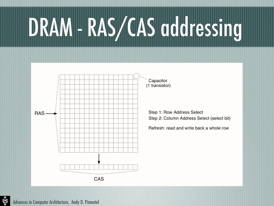
6 Components - DRAM DRAM - is a very dense form of RAM - it is volatile access is destructive & data must be re-written charge also leaks from the capacitor which stores the data so data must be refreshed periodically ( dynamic RAM) Typical DRAM chip characteristics Mbit and 2-800MHz cycle Uses two cycle Row/Column addressing (RAS/CAS) two-stage access and requirement to rewrite data contribute to slow cycle time but good design can help for regular accesses

7 DRAM - RAS/CAS addressing
8 DRAM refresh Voltage for 1 1 Written Refreshed Refreshed Refreshed Threshold voltage Voltage for 0 0 Stored 10s of ms before needing refresh cycle Time

9 Components - SRAM SRAM - is less dense but faster than DRAM uses four transistors to store data and two transistors to access it - access is non-destructive data is stable while the RAM has power connected ( static RAM) Typical SRAM chip characteristics ~64Mbit and 100MHz-1GHz cycle although SRAM cycle times are similar to DRAM, SRAM is true random access memory DRAM can only read consecutive bits at the cycle rate, therefore DRAM has a much larger latency time SRAM is also used for memory on the processor chip registers and cache both use SRAM technology the smaller the memory the faster it operates: lower latency

10 New technology Memristor a circuit element in which the resistance is a function of the history of the current through the device Memristor theory was formulated and named by Leon Chua in 1971 Ref: Chua, Leon O (1971), "Memristor -The Missing Circuit Element", IEEE Transactions on Circuit Theory CT-18 (5): , doi: /tct HP announced they teamed up with Hynix to produce a commercial product dubbed "ReRam" August has the potential to be dense and non-volatile

11 Bandwidth vs. Latency Memory latency is the time delay required to obtain a specific item of data This is larger in DRAM than in SRAM SRAM can access any bit each cycle DRAM is restricted to bits in the same row, CAS cycles Memory Bandwidth is the rate at which data can be accessed (e.g. bits per second) Bandwidth unit is normally 1/cycle time This rate can be improved by concurrent access

12 Improving DRAM bandwidth Using locality to get maximum bandwidth One RAS multiple CAS e.g. Fast page mode DRAM E(xtended) D(ata) O(utput) RAMs Burst-mode DRAMs Burst EDO RAM S(ynchronous)DRAM By improving the interface DDR SDRAM and RAMBUS
DRAM By")
13 Example - Synchronous DRAM SDRAM changed the memory interface from asynchronous to synchronous and uses a form of pipelining will return to this concept later DDR SDRAM - double data rate uses transfers on both rising and falling clock edges

14 Despite the performance improvement in the overall system due to use of SDRAM, the growing performance gap between the memory and processor must be filled by more advanced memory Different technologies. These technologies, SDRAM which are described technologies on the following pages, boost the overall performance of systems using the latest high-speed processors (Figure 8). Figure 8. Peak bandwidth comparison of SDRAM and advanced SDRAM technologies
. Figure 8.")
15 RAMBUS DRAMs This is an interface improvement using a pipelined bus interface sometimes called a split-transaction Bus comprises row and column address line + 18 bits of data 3 transactions on bus simultaneously (RAS/CAS/Data) High clock rate (400MHz) with data transfers on both edges Note that neither technique (SDRAM or RAMBUS) can improve the latency to access a single item of data
 can improve the latency to access a single item of")
16 Flash memory S o u r c e l i n e s Control gate Floating gate Source Word lines n p substrate n+ B i t l i n e s Drain

17 Memory wall solutions The most common solution to the memory wall is to cache data requires locality of access or memory reuse compiler optimisations can help to localise data Can also design banked memory systems to provide high bandwidth to random memory locations Some access patterns will still break the memory Can design processors that tolerate high-latency memory accesses don t wait do something else Requires concurrency in instruction execution

18 Summary Need for new dense + fast technology Most common solution: cache data Requires locality of access, or memory reuse Design processors that tolerate high-latency memory accesses don t wait do something else Trend: hardware multithreading in current and future chips

19 Summary Limits of RAM components cause Memory wall problem Caches & hw multithreading solutions New components (?)

Computer Architecture
 Computer Architecture Random Access Memory Technologies 2015. április 2. Budapest Gábor Horváth associate professor BUTE Dept. Of Networked Systems and Services [email protected] 2 Storing data Possible
A N. O N Output/Input-output connection
 Memory Types Two basic types: ROM: Read-only memory RAM: Read-Write memory Four commonly used memories: ROM Flash, EEPROM Static RAM (SRAM) Dynamic RAM (DRAM), SDRAM, RAMBUS, DDR RAM Generic pin configuration:
Computer Systems Structure Main Memory Organization
 Computer Systems Structure Main Memory Organization Peripherals Computer Central Processing Unit Main Memory Computer Systems Interconnection Communication lines Input Output Ward 1 Ward 2 Storage/Memory
RAM & ROM Based Digital Design. ECE 152A Winter 2012
 RAM & ROM Based Digital Design ECE 152A Winter 212 Reading Assignment Brown and Vranesic 1 Digital System Design 1.1 Building Block Circuits 1.1.3 Static Random Access Memory (SRAM) 1.1.4 SRAM Blocks in
Homework # 2. Solutions. 4.1 What are the differences among sequential access, direct access, and random access?
 ECE337 / CS341, Fall 2005 Introduction to Computer Architecture and Organization Instructor: Victor Manuel Murray Herrera Date assigned: 09/19/05, 05:00 PM Due back: 09/30/05, 8:00 AM Homework # 2 Solutions
Memory Basics. SRAM/DRAM Basics
 Memory Basics RAM: Random Access Memory historically defined as memory array with individual bit access refers to memory with both Read and Write capabilities ROM: Read Only Memory no capabilities for
Chapter 5 :: Memory and Logic Arrays
 Chapter 5 :: Memory and Logic Arrays Digital Design and Computer Architecture David Money Harris and Sarah L. Harris Copyright 2007 Elsevier 5- ROM Storage Copyright 2007 Elsevier 5- ROM Logic Data
SOLVING HIGH-SPEED MEMORY INTERFACE CHALLENGES WITH LOW-COST FPGAS
 SOLVING HIGH-SPEED MEMORY INTERFACE CHALLENGES WITH LOW-COST FPGAS A Lattice Semiconductor White Paper May 2005 Lattice Semiconductor 5555 Northeast Moore Ct. Hillsboro, Oregon 97124 USA Telephone: (503)
Module 2. Embedded Processors and Memory. Version 2 EE IIT, Kharagpur 1
 Module 2 Embedded Processors and Memory Version 2 EE IIT, Kharagpur 1 Lesson 5 Memory-I Version 2 EE IIT, Kharagpur 2 Instructional Objectives After going through this lesson the student would Pre-Requisite
Memory unit. 2 k words. n bits per word
 9- k address lines Read n data input lines Memory unit 2 k words n bits per word n data output lines 24 Pearson Education, Inc M Morris Mano & Charles R Kime 9-2 Memory address Binary Decimal Memory contents
Memory. The memory types currently in common usage are:
 ory ory is the third key component of a microprocessor-based system (besides the CPU and I/O devices). More specifically, the primary storage directly addressed by the CPU is referred to as main memory
Memory ICS 233. Computer Architecture and Assembly Language Prof. Muhamed Mudawar
 Memory ICS 233 Computer Architecture and Assembly Language Prof. Muhamed Mudawar College of Computer Sciences and Engineering King Fahd University of Petroleum and Minerals Presentation Outline Random
Configuring Memory on the HP Business Desktop dx5150
 Configuring Memory on the HP Business Desktop dx5150 Abstract... 2 Glossary of Terms... 2 Introduction... 2 Main Memory Configuration... 3 Single-channel vs. Dual-channel... 3 Memory Type and Speed...
ADVANCED PROCESSOR ARCHITECTURES AND MEMORY ORGANISATION Lesson-17: Memory organisation, and types of memory
 ADVANCED PROCESSOR ARCHITECTURES AND MEMORY ORGANISATION Lesson-17: Memory organisation, and types of memory 1 1. Memory Organisation 2 Random access model A memory-, a data byte, or a word, or a double
Computer Architecture
 Computer Architecture Slide Sets WS 2013/2014 Prof. Dr. Uwe Brinkschulte M.Sc. Benjamin Betting Part 11 Memory Management Computer Architecture Part 11 page 1 of 44 Prof. Dr. Uwe Brinkschulte, M.Sc. Benjamin
Semiconductor Device Technology for Implementing System Solutions: Memory Modules
 Hitachi Review Vol. 47 (1998), No. 4 141 Semiconductor Device Technology for Implementing System Solutions: Memory Modules Toshio Sugano Atsushi Hiraishi Shin ichi Ikenaga ABSTRACT: New technology is producing
Understanding Memory TYPES OF MEMORY
 Understanding Memory TYPES OF MEMORY In this study unit, you ll learn about physical and logical memory. Physical memory comes in two types, random access memory (RAM) and read-only memory (ROM). Typically,
Chapter 2 Basic Structure of Computers. Jin-Fu Li Department of Electrical Engineering National Central University Jungli, Taiwan
 Chapter 2 Basic Structure of Computers Jin-Fu Li Department of Electrical Engineering National Central University Jungli, Taiwan Outline Functional Units Basic Operational Concepts Bus Structures Software
Random-Access Memory (RAM) The Memory Hierarchy. SRAM vs DRAM Summary. Conventional DRAM Organization. Page 1
 The Memory Hierarchy. SRAM vs DRAM Summary. Conventional DRAM Organization. Page 1") Random-ccess Memor (RM) The Memor Hierarch Topics Storage technologies and trends Localit of reference Caching in the hierarch Ke features RM is packaged as a chip. Basic storage unit is a cell (one bit
Random-ccess Memor (RM) The Memor Hierarch Topics Storage technologies and trends Localit of reference Caching in the hierarch Ke features RM is packaged as a chip. Basic storage unit is a cell (one bit
Switch Fabric Implementation Using Shared Memory
 Order this document by /D Switch Fabric Implementation Using Shared Memory Prepared by: Lakshmi Mandyam and B. Kinney INTRODUCTION Whether it be for the World Wide Web or for an intra office network, today
Features. DDR SODIMM Product Datasheet. Rev. 1.0 Oct. 2011
 Features 200pin, unbuffered small outline dual in-line memory module (SODIMM) Fast data transfer rates: PC-2100, PC-2700, PC3-3200 Single or Dual rank 256MB(32Megx64), 512MB (64Meg x 64), 1GB(128 Meg x
Chapter 6. Inside the System Unit. What You Will Learn... Computers Are Your Future. What You Will Learn... Describing Hardware Performance
 What You Will Learn... Computers Are Your Future Chapter 6 Understand how computers represent data Understand the measurements used to describe data transfer rates and data storage capacity List the components
Table 1: Address Table
 DDR SDRAM DIMM D32PB12C 512MB D32PB1GJ 1GB For the latest data sheet, please visit the Super Talent Electronics web site: www.supertalentmemory.com Features 184-pin, dual in-line memory module (DIMM) Fast
Memory Hierarchy. Arquitectura de Computadoras. Centro de Investigación n y de Estudios Avanzados del IPN. [email protected]. MemoryHierarchy- 1
 Hierarchy Arturo Díaz D PérezP Centro de Investigación n y de Estudios Avanzados del IPN [email protected] Hierarchy- 1 The Big Picture: Where are We Now? The Five Classic Components of a Computer Processor
Open Flow Controller and Switch Datasheet
 Open Flow Controller and Switch Datasheet California State University Chico Alan Braithwaite Spring 2013 Block Diagram Figure 1. High Level Block Diagram The project will consist of a network development
Objectives. Units of Memory Capacity. CMPE328 Microprocessors (Spring 2007-08) Memory and I/O address Decoders. By Dr.
 Memory and I/O address Decoders. By Dr.") CMPE328 Microprocessors (Spring 27-8) Memory and I/O address ecoders By r. Mehmet Bodur You will be able to: Objectives efine the capacity, organization and types of the semiconductor memory devices Calculate
CMPE328 Microprocessors (Spring 27-8) Memory and I/O address ecoders By r. Mehmet Bodur You will be able to: Objectives efine the capacity, organization and types of the semiconductor memory devices Calculate
Byte Ordering of Multibyte Data Items
 Byte Ordering of Multibyte Data Items Most Significant Byte (MSB) Least Significant Byte (LSB) Big Endian Byte Addresses +0 +1 +2 +3 +4 +5 +6 +7 VALUE (8-byte) Least Significant Byte (LSB) Most Significant
The Central Processing Unit:
 The Central Processing Unit: What Goes on Inside the Computer Chapter 4 Objectives Identify the components of the central processing unit and how they work together and interact with memory Describe how
Random Access Memory (RAM) Types of RAM. RAM Random Access Memory Jamie Tees SDRAM. Micro-DIMM SO-DIMM
 Types of RAM. RAM Random Access Memory Jamie Tees SDRAM. Micro-DIMM SO-DIMM") Random Access Memory (RAM) Sends/Receives data quickly between CPU This is way quicker than using just the HDD RAM holds temporary data used by any open application or active / running process Multiple
Random Access Memory (RAM) Sends/Receives data quickly between CPU This is way quicker than using just the HDD RAM holds temporary data used by any open application or active / running process Multiple
With respect to the way of data access we can classify memories as:
 Memory Classification With respect to the way of data access we can classify memories as: - random access memories (RAM), - sequentially accessible memory (SAM), - direct access memory (DAM), - contents
CHAPTER 7: The CPU and Memory
 CHAPTER 7: The CPU and Memory The Architecture of Computer Hardware, Systems Software & Networking: An Information Technology Approach 4th Edition, Irv Englander John Wiley and Sons 2010 PowerPoint slides
NAND Flash FAQ. Eureka Technology. apn5_87. NAND Flash FAQ
 What is NAND Flash? What is the major difference between NAND Flash and other Memory? Structural differences between NAND Flash and NOR Flash What does NAND Flash controller do? How to send command to
User s Manual HOW TO USE DDR SDRAM
 User s Manual HOW TO USE DDR SDRAM Document No. E0234E30 (Ver.3.0) Date Published April 2002 (K) Japan URL: http://www.elpida.com Elpida Memory, Inc. 2002 INTRODUCTION This manual is intended for users
Price/performance Modern Memory Hierarchy
 Lecture 21: Storage Administration Take QUIZ 15 over P&H 6.1-4, 6.8-9 before 11:59pm today Project: Cache Simulator, Due April 29, 2010 NEW OFFICE HOUR TIME: Tuesday 1-2, McKinley Last Time Exam discussion
Algorithms and Methods for Distributed Storage Networks 3. Solid State Disks Christian Schindelhauer
 Algorithms and Methods for Distributed Storage Networks 3. Solid State Disks Institut für Informatik Wintersemester 2007/08 Solid State Disks Motivation 2 10 5 1980 1985 1990 1995 2000 2005 2010 PRODUCTION
Memory Basics ~ ROM, DRAM, SRAM, Cache Memory The article was added by Kyle Duke
 Page 1 of 5 Memory Basics ~ ROM, DRAM, SRAM, Cache Memory The article was added by Kyle Duke Memory is the workspace for the computer's processor. It is a temporary storage area where the programs and
Low Power AMD Athlon 64 and AMD Opteron Processors
 Low Power AMD Athlon 64 and AMD Opteron Processors Hot Chips 2004 Presenter: Marius Evers Block Diagram of AMD Athlon 64 and AMD Opteron Based on AMD s 8 th generation architecture AMD Athlon 64 and AMD
RAM. Overview DRAM. What RAM means? DRAM
 Overview RAM In this chapter, you will learn how to Identify the different types of RAM packaging Explain the varieties of DRAM Install RAM properly Perform basic RAM troubleshooting Program Execution
Chapter 9 Semiconductor Memories. Jin-Fu Li Department of Electrical Engineering National Central University Jungli, Taiwan
 Chapter 9 Semiconductor Memories Jin-Fu Li Department of Electrical Engineering National Central University Jungli, Taiwan Advanced Reliable Systems (ARES) Lab. Jin-Fu Li, EE, NCU 2 Outline Introduction
361 Computer Architecture Lecture 14: Cache Memory
 1 361 Computer Architecture Lecture 14 Memory cache.1 The Motivation for s Memory System Processor DRAM Motivation Large memories (DRAM) are slow Small memories (SRAM) are fast Make the average access
Chapter 2: Computer-System Structures. Computer System Operation Storage Structure Storage Hierarchy Hardware Protection General System Architecture
 Chapter 2: Computer-System Structures Computer System Operation Storage Structure Storage Hierarchy Hardware Protection General System Architecture Operating System Concepts 2.1 Computer-System Architecture
Computer-System Architecture
 Chapter 2: Computer-System Structures Computer System Operation I/O Structure Storage Structure Storage Hierarchy Hardware Protection General System Architecture 2.1 Computer-System Architecture 2.2 Computer-System
Memory technology evolution: an overview of system memory technologies
 Memory technology evolution: an overview of system memory technologies Technology brief, 9 th edition Introduction... 2 Basic DRAM operation... 2 DRAM storage density and power consumption... 4 Memory
CSCA0102 IT & Business Applications. Foundation in Business Information Technology School of Engineering & Computing Sciences FTMS College Global
 CSCA0102 IT & Business Applications Foundation in Business Information Technology School of Engineering & Computing Sciences FTMS College Global Chapter 2 Data Storage Concepts System Unit The system unit
Logical Operations. Control Unit. Contents. Arithmetic Operations. Objectives. The Central Processing Unit: Arithmetic / Logic Unit.
 Objectives The Central Processing Unit: What Goes on Inside the Computer Chapter 4 Identify the components of the central processing unit and how they work together and interact with memory Describe how
Slide Set 8. for ENCM 369 Winter 2015 Lecture Section 01. Steve Norman, PhD, PEng
 Slide Set 8 for ENCM 369 Winter 2015 Lecture Section 01 Steve Norman, PhD, PEng Electrical & Computer Engineering Schulich School of Engineering University of Calgary Winter Term, 2015 ENCM 369 W15 Section
COMPUTER HARDWARE. Input- Output and Communication Memory Systems
 COMPUTER HARDWARE Input- Output and Communication Memory Systems Computer I/O I/O devices commonly found in Computer systems Keyboards Displays Printers Magnetic Drives Compact disk read only memory (CD-ROM)
Atmel Norway 2005. XMEGA Introduction
 Atmel Norway 005 XMEGA Introduction XMEGA XMEGA targets Leadership on Peripheral Performance Leadership in Low Power Consumption Extending AVR market reach XMEGA AVR family 44-100 pin packages 16K 51K
White Paper Utilizing Leveling Techniques in DDR3 SDRAM Memory Interfaces
 White Paper Introduction The DDR3 SDRAM memory architectures support higher bandwidths with bus rates of 600 Mbps to 1.6 Gbps (300 to 800 MHz), 1.5V operation for lower power, and higher densities of 2
Agenda. Michele Taliercio, Il circuito Integrato, Novembre 2001
 Agenda Introduzione Il mercato Dal circuito integrato al System on a Chip (SoC) La progettazione di un SoC La tecnologia Una fabbrica di circuiti integrati 28 How to handle complexity G The engineering
Computers. Hardware. The Central Processing Unit (CPU) CMPT 125: Lecture 1: Understanding the Computer
 CMPT 125: Lecture 1: Understanding the Computer") Computers CMPT 125: Lecture 1: Understanding the Computer Tamara Smyth, [email protected] School of Computing Science, Simon Fraser University January 3, 2009 A computer performs 2 basic functions: 1.
Computers CMPT 125: Lecture 1: Understanding the Computer Tamara Smyth, [email protected] School of Computing Science, Simon Fraser University January 3, 2009 A computer performs 2 basic functions: 1.
DDR4 Memory Technology on HP Z Workstations
 Technical white paper DDR4 Memory Technology on HP Z Workstations DDR4 is the latest memory technology available for main memory on mobile, desktops, workstations, and server computers. DDR stands for
Technical Note. Initialization Sequence for DDR SDRAM. Introduction. Initializing DDR SDRAM
 TN-46-8: Initialization Sequence for DDR SDRAM Introduction Technical Note Initialization Sequence for DDR SDRAM Introduction The double data rate DDR synchronous dynamic random access memory SDRAM device
Memory Systems. Static Random Access Memory (SRAM) Cell
 Cell") Memory Systems This chapter begins the discussion of memory systems from the implementation of a single bit. The architecture of memory chips is then constructed using arrays of bit implementations coupled
Memory Systems This chapter begins the discussion of memory systems from the implementation of a single bit. The architecture of memory chips is then constructed using arrays of bit implementations coupled
ThinkServer PC3-10600 DDR3 1333MHz UDIMM and RDIMM PC3-8500 DDR3 1066MHz RDIMM options for the next generation of ThinkServer systems TS200 and RS210
 Hardware Announcement ZG09-0894, dated vember 24, 2009 ThinkServer PC3-10600 DDR3 1333MHz UDIMM and RDIMM PC3-8500 DDR3 1066MHz RDIMM options for the next generation of ThinkServer systems TS200 and RS210
Technical Note. Micron NAND Flash Controller via Xilinx Spartan -3 FPGA. Overview. TN-29-06: NAND Flash Controller on Spartan-3 Overview
 Technical Note TN-29-06: NAND Flash Controller on Spartan-3 Overview Micron NAND Flash Controller via Xilinx Spartan -3 FPGA Overview As mobile product capabilities continue to expand, so does the demand
Am186ER/Am188ER AMD Continues 16-bit Innovation
 Am186ER/Am188ER AMD Continues 16-bit Innovation 386-Class Performance, Enhanced System Integration, and Built-in SRAM Problem with External RAM All embedded systems require RAM Low density SRAM moving
OpenSPARC T1 Processor
 OpenSPARC T1 Processor The OpenSPARC T1 processor is the first chip multiprocessor that fully implements the Sun Throughput Computing Initiative. Each of the eight SPARC processor cores has full hardware
AMD Opteron Quad-Core
 AMD Opteron Quad-Core a brief overview Daniele Magliozzi Politecnico di Milano Opteron Memory Architecture native quad-core design (four cores on a single die for more efficient data sharing) enhanced
1.1 Silicon on Insulator a brief Introduction
 Table of Contents Preface Acknowledgements Chapter 1: Overview 1.1 Silicon on Insulator a brief Introduction 1.2 Circuits and SOI 1.3 Technology and SOI Chapter 2: SOI Materials 2.1 Silicon on Heteroepitaxial
A New Chapter for System Designs Using NAND Flash Memory
 A New Chapter for System Designs Using Memory Jim Cooke Senior Technical Marketing Manager Micron Technology, Inc December 27, 2010 Trends and Complexities trends have been on the rise since was first
ADQYF1A08. DDR2-1066G(CL6) 240-Pin O.C. U-DIMM 1GB (128M x 64-bits)
 240-Pin O.C. U-DIMM 1GB (128M x 64-bits)") General Description ADQYF1A08 DDR2-1066G(CL6) 240-Pin O.C. U-DIMM 1GB (128M x 64-bits) The ADATA s ADQYF1A08 is a 128Mx64 bits 1GB DDR2-1066(CL6) SDRAM over clocking memory module, The SPD is programmed
General Description ADQYF1A08 DDR2-1066G(CL6) 240-Pin O.C. U-DIMM 1GB (128M x 64-bits) The ADATA s ADQYF1A08 is a 128Mx64 bits 1GB DDR2-1066(CL6) SDRAM over clocking memory module, The SPD is programmed
Semiconductor Memories
 Semiconductor Memories Semiconductor memories array capable of storing large quantities of digital information are essential to all digital systems Maximum realizable data storage capacity of a single
Chapter 6. 6.1 Introduction. Storage and Other I/O Topics. p. 570( 頁 585) Fig. 6.1. I/O devices can be characterized by. I/O bus connections
 Fig. 6.1. I/O devices can be characterized by. I/O bus connections") Chapter 6 Storage and Other I/O Topics 6.1 Introduction I/O devices can be characterized by Behavior: input, output, storage Partner: human or machine Data rate: bytes/sec, transfers/sec I/O bus connections
Chapter 6 Storage and Other I/O Topics 6.1 Introduction I/O devices can be characterized by Behavior: input, output, storage Partner: human or machine Data rate: bytes/sec, transfers/sec I/O bus connections
NTE2053 Integrated Circuit 8 Bit MPU Compatible A/D Converter
 NTE2053 Integrated Circuit 8 Bit MPU Compatible A/D Converter Description: The NTE2053 is a CMOS 8 bit successive approximation Analog to Digital converter in a 20 Lead DIP type package which uses a differential
DDR3 memory technology
 DDR3 memory technology Technology brief, 3 rd edition Introduction... 2 DDR3 architecture... 2 Types of DDR3 DIMMs... 2 Unbuffered and Registered DIMMs... 2 Load Reduced DIMMs... 3 LRDIMMs and rank multiplication...
Chapter 7 Memory and Programmable Logic
 NCNU_2013_DD_7_1 Chapter 7 Memory and Programmable Logic 71I 7.1 Introduction ti 7.2 Random Access Memory 7.3 Memory Decoding 7.5 Read Only Memory 7.6 Programmable Logic Array 77P 7.7 Programmable Array
Lecture 3: Modern GPUs A Hardware Perspective Mohamed Zahran (aka Z) [email protected] http://www.mzahran.com
 mzahran@cs.nyu.edu http://www.mzahran.com") CSCI-GA.3033-012 Graphics Processing Units (GPUs): Architecture and Programming Lecture 3: Modern GPUs A Hardware Perspective Mohamed Zahran (aka Z) [email protected] http://www.mzahran.com Modern GPU
CSCI-GA.3033-012 Graphics Processing Units (GPUs): Architecture and Programming Lecture 3: Modern GPUs A Hardware Perspective Mohamed Zahran (aka Z) [email protected] http://www.mzahran.com Modern GPU
Class 18: Memories-DRAMs
 Topics: 1. Introduction 2. Advantages and Disadvantages of DRAMs 3. Evolution of DRAMs 4. Evolution of DRAMs 5. Basics of DRAMs 6. Basics of DRAMs 7. Write Operation 8. SA-Normal Operation 9. SA-Read Operation
Modeling Sequential Elements with Verilog. Prof. Chien-Nan Liu TEL: 03-4227151 ext:34534 Email: [email protected]. Sequential Circuit
 Modeling Sequential Elements with Verilog Prof. Chien-Nan Liu TEL: 03-4227151 ext:34534 Email: [email protected] 4-1 Sequential Circuit Outputs are functions of inputs and present states of storage elements
Intel 965 Express Chipset Family Memory Technology and Configuration Guide
 Intel 965 Express Chipset Family Memory Technology and Configuration Guide White Paper - For the Intel 82Q965, 82Q963, 82G965 Graphics and Memory Controller Hub (GMCH) and Intel 82P965 Memory Controller
Lecture 9: Memory and Storage Technologies
 CS61: Systems Programming and Machine Organization Harvard University, Fall 2009 Lecture 9: Memory and Storage Technologies October 1, 2009 Announcements Lab 3 has been released! You are welcome to switch
Lecture 2: Computer Hardware and Ports. [email protected] http://faculty.sau.edu.sa/y.alharbi/en
 BMTS 242: Computer and Systems Lecture 2: Computer Hardware and Ports Yousef Alharbi Email Website [email protected] http://faculty.sau.edu.sa/y.alharbi/en The System Unit McGraw-Hill Copyright 2011
SLC vs. MLC: An Analysis of Flash Memory
 SLC vs. MLC: An Analysis of Flash Memory Examining the Quality of Memory: Understanding the Differences between Flash Grades Table of Contents Abstract... 3 Introduction... 4 Flash Memory Explained...
COMPUTER SCIENCE AND ENGINEERING - Microprocessor Systems - Mitchell Aaron Thornton
 MICROPROCESSOR SYSTEMS Mitchell Aaron Thornton, Department of Electrical and Computer Engineering, Mississippi State University, PO Box 9571, Mississippi State, MS, 39762-9571, United States. Keywords:
Table 1 SDR to DDR Quick Reference
 TECHNICAL NOTE TN-6-05 GENERAL DDR SDRAM FUNCTIONALITY INTRODUCTION The migration from single rate synchronous DRAM (SDR) to double rate synchronous DRAM (DDR) memory is upon us. Although there are many
GR2DR4B-EXXX/YYY/LP 1GB & 2GB DDR2 REGISTERED DIMMs (LOW PROFILE)
") GENERAL DESCRIPTION The Gigaram is a 128M/256M bit x 72 DDDR2 SDRAM high density JEDEC standard ECC Registered memory module. The Gigaram consists of eighteen CMOS 128MX4 DDR2 for 1GB and thirty-six CMOS
GENERAL DESCRIPTION The Gigaram is a 128M/256M bit x 72 DDDR2 SDRAM high density JEDEC standard ECC Registered memory module. The Gigaram consists of eighteen CMOS 128MX4 DDR2 for 1GB and thirty-six CMOS
Introduction To Computers: Hardware and Software
 What Is Hardware? Introduction To Computers: Hardware and Software A computer is made up of hardware. Hardware is the physical components of a computer system e.g., a monitor, keyboard, mouse and the computer
The Quest for Speed - Memory. Cache Memory. A Solution: Memory Hierarchy. Memory Hierarchy
 The Quest for Speed - Memory Cache Memory CSE 4, Spring 25 Computer Systems http://www.cs.washington.edu/4 If all memory accesses (IF/lw/sw) accessed main memory, programs would run 20 times slower And
Communicating with devices
 Introduction to I/O Where does the data for our CPU and memory come from or go to? Computers communicate with the outside world via I/O devices. Input devices supply computers with data to operate on.
Technical Product Specifications Dell Dimension 2400 Created by: Scott Puckett
 Technical Product Specifications Dell Dimension 2400 Created by: Scott Puckett Page 1 of 11 Table of Contents Technical Product Specifications Model 3 PC Technical Diagrams Front Exterior Specifications
Computing for Data-Intensive Applications:
 Computing for Data-Intensive Applications: Beyond CMOS and Beyond Von-Neumann Said Hamdioui Computer Engineering Delft University of Technology The Netherlands Workshop on Memristive systems for Space
Storage Class Memory and the data center of the future
 IBM Almaden Research Center Storage Class Memory and the data center of the future Rich Freitas HPC System performance trends System performance requirement has historically double every 18 mo and this
7a. System-on-chip design and prototyping platforms
 7a. System-on-chip design and prototyping platforms Labros Bisdounis, Ph.D. Department of Computer and Communication Engineering 1 What is System-on-Chip (SoC)? System-on-chip is an integrated circuit
McPAT: An Integrated Power, Area, and Timing Modeling Framework for Multicore and Manycore Architectures
 McPAT: An Integrated Power, Area, and Timing Modeling Framework for Multicore and Manycore Architectures Sheng Li, Junh Ho Ahn, Richard Strong, Jay B. Brockman, Dean M Tullsen, Norman Jouppi MICRO 2009
Lizy Kurian John Electrical and Computer Engineering Department, The University of Texas as Austin
 BUS ARCHITECTURES Lizy Kurian John Electrical and Computer Engineering Department, The University of Texas as Austin Keywords: Bus standards, PCI bus, ISA bus, Bus protocols, Serial Buses, USB, IEEE 1394
TECHNOLOGY BRIEF. Compaq RAID on a Chip Technology EXECUTIVE SUMMARY CONTENTS
 TECHNOLOGY BRIEF August 1999 Compaq Computer Corporation Prepared by ISSD Technology Communications CONTENTS Executive Summary 1 Introduction 3 Subsystem Technology 3 Processor 3 SCSI Chip4 PCI Bridge
Intel X38 Express Chipset Memory Technology and Configuration Guide
 Intel X38 Express Chipset Memory Technology and Configuration Guide White Paper January 2008 Document Number: 318469-002 INFORMATION IN THIS DOCUMENT IS PROVIDED IN CONNECTION WITH INTEL PRODUCTS. NO LICENSE,
Intel Q35/Q33, G35/G33/G31, P35/P31 Express Chipset Memory Technology and Configuration Guide
 Intel Q35/Q33, G35/G33/G31, P35/P31 Express Chipset Memory Technology and Configuration Guide White Paper August 2007 Document Number: 316971-002 INFORMATION IN THIS DOCUMENT IS PROVIDED IN CONNECTION
In-Memory Databases Algorithms and Data Structures on Modern Hardware. Martin Faust David Schwalb Jens Krüger Jürgen Müller
 In-Memory Databases Algorithms and Data Structures on Modern Hardware Martin Faust David Schwalb Jens Krüger Jürgen Müller The Free Lunch Is Over 2 Number of transistors per CPU increases Clock frequency
Bandwidth Calculations for SA-1100 Processor LCD Displays
 Bandwidth Calculations for SA-1100 Processor LCD Displays Application Note February 1999 Order Number: 278270-001 Information in this document is provided in connection with Intel products. No license,
Why Latency Lags Bandwidth, and What it Means to Computing
 Why Latency Lags Bandwidth, and What it Means to Computing David Patterson U.C. Berkeley [email protected] October 2004 Bandwidth Rocks (1) Preview: Latency Lags Bandwidth Over last 20 to 25 years,
QUICK START GUIDE FOR DEMONSTRATION CIRCUIT 956 24-BIT DIFFERENTIAL ADC WITH I2C LTC2485 DESCRIPTION
 LTC2485 DESCRIPTION Demonstration circuit 956 features the LTC2485, a 24-Bit high performance Σ analog-to-digital converter (ADC). The LTC2485 features 2ppm linearity, 0.5µV offset, and 600nV RMS noise.
Driving The Need For Innovative Memory Solutions
 Driving The Need For Innovative Memory Solutions Dr. Ronald D. Black President & CEO 3 February 2014 Quote When a management with a reputation for brilliance tackles a business with a reputation for bad
Unit A451: Computer systems and programming. Section 2: Computing Hardware 1/5: Central Processing Unit
 Unit A451: Computer systems and programming Section 2: Computing Hardware 1/5: Central Processing Unit Section Objectives Candidates should be able to: (a) State the purpose of the CPU (b) Understand the
EE482: Advanced Computer Organization Lecture #11 Processor Architecture Stanford University Wednesday, 31 May 2000. ILP Execution
 EE482: Advanced Computer Organization Lecture #11 Processor Architecture Stanford University Wednesday, 31 May 2000 Lecture #11: Wednesday, 3 May 2000 Lecturer: Ben Serebrin Scribe: Dean Liu ILP Execution
Computer Organization. and Instruction Execution. August 22
 Computer Organization and Instruction Execution August 22 CSC201 Section 002 Fall, 2000 The Main Parts of a Computer CSC201 Section Copyright 2000, Douglas Reeves 2 I/O and Storage Devices (lots of devices,
Mobile SDRAM. MT48H16M16LF 4 Meg x 16 x 4 banks MT48H8M32LF 2 Meg x 32 x 4 banks
 Features Mobile SDRAM MT48H6M6LF 4 Meg x 6 x 4 banks MT48H8M32LF 2 Meg x 32 x 4 banks Features Fully synchronous; all signals registered on positive edge of system clock V DD /V D =.7.95V Internal, pipelined
1.55V DDR2 SDRAM FBDIMM
 1.55V DDR2 SDRAM FBDIMM MT18RTF25672FDZ 2GB 2GB (x72, DR) 240-Pin DDR2 SDRAM FBDIMM Features Features 240-pin, fully buffered DIMM (FBDIMM) Very low-power DDR2 operation Component configuration: 256 Meg
Power-Aware High-Performance Scientific Computing
 Power-Aware High-Performance Scientific Computing Padma Raghavan Scalable Computing Laboratory Department of Computer Science Engineering The Pennsylvania State University http://www.cse.psu.edu/~raghavan