High-Speed Electronics
|
|
|
- Jasper Williamson
- 10 years ago
- Views:
Transcription
1 High-Speed Electronics Mentor User Conference München Dr. Alex Huber, [email protected] Zentrum für Mikroelektronik Aargau, 5210 Windisch, Switzerland Page 1

2 Outline 1. Motivation 2. Speed Limitation of CMOS logic 3. Current Mode Logic: Advantages and Features 4. Current Mode Logic Gates 5. Example Application: Clock-Data Recovery 6. Conclusion Page 2

3 1. Motivation 2. Speed Limitation of CMOS logic 3. Current Mode Logic: Advantages and Features 4. Current Mode Logic Gates 5. Example Application: Clock-Data Recovery 6. Conclusion Page 3

4 Applications Serial Data Communication (PCI-Express, Serial-ATA, etc.) Fiber-Optical Communication (e.g. 10G Ethernet) Flash-ADC, high-speed Σ -ADC Ultra-Wideband (UWB) = wireless digital interconnect Fractional-N PLL (Prescaler) Page 4
 = wireless digital interconnect Fractional-N PLL")
5 Parallel I/O Bottleneck CPU Graphics-P. Display Harddisk Memory 64bit, 3GHz D0 D1 Dn CLK f CLK C coup X-Talk Clock/Data Skew Clock Jitter Data Jitter D0 D1 Dn CLK f CLK < l = 1 m 10 cm, 16 64bit CPU Graphics-P. Display Harddisk Memory 64bit, 3GHz Internal throughput: 24GByte/s I/O throughput: 1 4 GByte/s m Page 5

6 Serial Data Communication D0 D1 Dn CLK f CLK MUX f ser D 0 f CLK = 2 GHz, n = 16 bit Clock not transmitted: f CLK = 2 GHz, n = 64 bit D 1 D 2D3 f ser = n/2 f CLK f CLK D n DEC f ser CR DEMUX 2/n High-Speed Digital Electronics required! f CLK D0 D1 Dn CLK CLK generated at Rx f SER = 8 2 GHz = 16 GHz (32 Gb/s) Unlimited number of parallel links 4 links à 32 Gb/s: 128 Gb/s = 16GB/s Page 6
 Unlimited number of")
7 I/O Technology Trend 20GHz 10GHz 5GHz 1GHz 66MHz PCI Bus VESA MCA EISA ISA Bus Page 7 f SER = signaling clock rate 12GHz Copper Signaling Limit (attenuation) Serial Bus Architectures 1GHz Parallel Bus Limit (cross-talk) PCI-X AGP 2x Optical PCI Express Serial-ATA IEEE 1394b Parallel Bus Architectures Year Source: National Instruments

8 Technologies Earlier: Dominated by bipolar processes (GaAs, Si, SiGe, InP) Nowadays: CMOS at 130nm, 90nm, (65nm) Question: How to reach > 10 GHz using CMOS technologies Page 8

9 1. Motivation 2. Speed Limitation of CMOS logic 3. Current Mode Logic: Advantages and Features 4. Current Mode Logic Gates 5. Example Application: Clock-Data Recovery 6. Conclusion Page 9

10 Repetion: Some Basics of MOSFET G V GS D S I D W n L DC Drain Current Transconductance Page 10 I V DS D V GS G S D I D W p L V DS ( ) W VGS UT = Cox µ n,p for VDS VGS UT L 2 g m I G S 2 C GS v GS g m v GS > i D C DS Threshold Voltage Design Variables W U = D = GS T 2 C µ ox n,p VGS L 2 V 0 D S

11 Speed Limitation of CMOS Gates V DD W p L C gs,p V gs,p C ds,p i d,p =g m,p *V gs,p V in Page 11 W n L V out With ideal voltage drive: V in C gs,n V gs,n t d = V out C ds,p /i d,n C ds,n i d,n =g m,n *V gs,n For V p =V DD /2: W p 2 3 W n (due to µ n 2...3µ p ) To reduce delay t d : C ds,p L ; W p W n i d,n L ; g m,n W n Technology scaling: L=1µm (1990) L=90nm (2004) Given technology: No improvement possible! V out
 To reduce delay t d : C ds,p L ; W p W n i d,n L ; g m,n W n Technology scaling: L=1µm (1990)")
12 Reduction of Delay Time Basic idea: Decouple charging current and switch transistor V DD Load Load: PMOS, resistor, inductor,? Page 12 V in W n L V out I charge ; W n t d i charge Common Mode Voltage V cm? Limits: W n large enough for a) V-Gain = g m,n R Load > 1 b) V ds,sat (i charge ) < V DD - V cm - V Load
 V-Gain = g m,n R Load > 1 b) V ds,sat (i")
13 Current Mode Logic (CML) Differential topology: independent of V cm V in Load V DD W n L V out V cm i 0 V DD Load W n L Advantages for high-speed operation: 1. Independent choice of W n and i 0 2. Differential mode: higher SNR 3. Free choice of load: PMOS, Resistor, Inductor 4. With Inductor: BW ind 2 BW res f CLK,CML (2..3) f same L Disadvantages: 1. Static DC power consumption V DD i 0 2. Area consumption: 2 {PMOS Res Ind}, 3 NMOS Page 13
 f CLK,CMOS @ same L Disadvantages: 1.")
14 1. Motivation 2. Speed Limitation of CMOS logic 3. Current Mode Logic: Advantages and Features 4. Current Mode Logic Gates 5. Example Application: Clock-Data Recovery 6. Conclusion Page 14

15 CML vs. CMOS: Figures of Merit Logic swing Load Capacitance Logic depth Delay t d N RC CML V C = N I C ox CMOS N C VDD µ V U ) ( DD t ~ V ~I α Power P Power- Delay Product Energy- Delay Product P t P t 2 d d = = N I V [ N I V ] = N 2 V DD DD DD 2 [ N V V C] = N DD 3 V DD V C N I V C N 2 2 ( V ) C I V C I N N V t 2 DD d, CMOS C ( f CLK = 1 t 2 VDD C td, CMOS 2 = N V t d, CMOS N V = C 2 DD ox C t d, CMOS N VDDC µ ( V U ) DD t α DD d ) C Page 15
![V U ) ( DD t ~ V ~I α Power P Power- Delay Product Energy- Delay Product P t P t 2 d d = = N I V [ N I V ] = N 2](/docs-images/43/5983664/images/page_15.jpg "V DD DD DD 2 [ N V V C] = N DD 3 V DD V C N I V C N 2 2 ( V ) C I V C I N N V t 2 DD d, CMOS C ( f CLK = 1 t 2")
16 CML vs. CMOS: Trade-Off Energy-Delay-Product EDP: EDP CMOS = C ox N VDDC µ ( V U ) DD t α EDP CML = N 3 V DD ( V ) I 2 C t d [ps] V DD [V] Page 16 Delay CMOS Advantage for CML: low logic depth, very high speed Example: 0.25µm technology V DD =2.5V PMOS load Energy-Delay (N=4) EDP [pj ps] t d [ps] 400 t d [ps] Delay CML I [µa] No low bound on CML delay with current! Source: An Analysis of MOS CML for Low Power and High Performance Digital Logic, Master thesis, J. Musicer, UC Berkeley
![100 0.5 1 1.5 2 V DD [V] Page 16 Delay CMOS Advantage for CML: low logic depth, very high speed Example: 0.25µm technology V DD =2.](/docs-images/43/5983664/images/page_16.jpg "5V PMOS load 2.5 2 1.")
17 1. Motivation 2. Speed Limitation of CMOS logic 3. Current Mode Logic: Advantages and Features 4. Current Mode Logic Gates 5. Example Application: Clock-Data Recovery 6. Conclusion Page 17

18 Inverter Page 18 V DD Logic Level: V h = I 0 R C t d Gate Delay

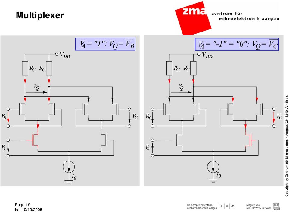
19 Multiplexer V DD V DD Page 19
20 EXOR V A =1, V B =1: V Q =-1~0 V A =-1, V B =1: V Q =1 Page 20 V DD V DD V A =1, V B =-1: V Q =1 V DD V DD V A =-1, V B =-1: V Q =-1~0

21 D-Latch VDD Page 21 V DD
22 Master-Slave D-FlipFlop Page 22 Negative edge triggered FF with respect to CLK
23 Design Techniques for CML CMOS design kits typically don t provide CML standard cells (some Bipolar/BiCMOS kits might, but typically only in very mature = old = slow technologies and only symbol/layout) System design can be done on cell-level Cell design is done with analog (= transistor-level) techniques Simulation must reflect the analog nature of CML gates (= dependence of delay/transition-time on input/output impedance) Good and useful design technique: VHDL-/Verilog-AMS Page 23
24 1. Motivation 2. Speed Limitation of CMOS logic 3. Current Mode Logic: Advantages and Features 4. Current Mode Logic Gates 5. Example: Clock-Data Recovery for Serial Data Communication 6. Conclusion Page 24
25 Clock-Data Recovery (I) D in DEC f ser CR Page 25 DEMUX D 0 D 1 D n 2/n CLK Analog Full-Rate Architecture D in DFF PFD LF VCO DFF (CML) and VCO operate at f ser (e.g. 40GHz at 40Gb/s) low complexity ultra-high-speed technology (SiGe, InP) required Passive, external? DEMUX PLL
26 Clock-Data Recovery (II) D in DEC f ser DEMUX D 0 D 1 D n n-th Rate Architecture 2n DFF Digital (CML) D 0 D 1 CR 2/n CLK Clock frequency at DFF: f CLK, full-rate /n 2n phases required ( t = 1/(2f CLK, full-rate )) D in 2n VCO Phases Analog (?) DFF DFF VCO Reference Frequency Edge Detector Loop Filter D n Page 26
27 Edge Detection 2n DFF D in DFF DFF d 0 e 0 e n Edge Detector 2n Phase Clk to Loop Filter locked: CLK in-phase with DATA CLK is early w/ respect to DATA CLK d 0 d 1 d n d n+1 D0 D1 D2 D3 DATA e 0 e 1 <e n > = 0.5 CLK CLK d 0 d 1 D0 D1 D2 D3 DATA d n = e n e 0 e 1 CLK Page 27
28 Generation of Variable Clock Phase VCO: V ctrl cos([ω 0 +K vco V ctrl ] t) = cos(ω 0 t + φ) φ = K vco V ctrl t = K vco V ctrl dt Phase Rotator: cos(ω 0 t) φ 1 φ n n-phase VCO UP DN δϕ φ-rot no Integration! ϕ = δϕ n T cos(ω 0 t + φ) I = ϕ 2 Q Q = ϕ 3 = ϕ 1 I = ϕ 0 Page 28
29 Clock-Data Recovery (III): HIGHSCORE High-Speed Communication Receiver for 40 Gb/s in CMOS : CTI Project of zma, BFH Burgdorf, ETHZ, IBM ZRL 40 Gb/s optical input 0, 45,..., 315 Page D Edge- Early Detector 16 E Late Phase- Rotator 8 parallel Sampler 8-phase DLL CML ( analog ) E D E D E D E D 8:32 DEMUX Rate Reduction Early Late GHz 2.5GHz 1.25GHz up up/down Digital Loop dn counter Filter 1.25GHz 0, 45,..., 315 Ref-VCO (8 phase) 1x for 8 Links 4 4x 10Gb/s electrical output 1x/Link CMOS ( digital )
30 HIGHSCORE Key Features Goal: Serial Communication Receiver (=CDR) at 40 Gb/s 90 nm CMOS state-of-the-art (IBM) FO4-Delay of CMOS: 20 ps Typical clock frequencies of CMOS logic: 1.25 GHz CML operates at f CLK = 10 GHz, partially inductor-peaked Quarter-Rate Architecture No external passive components (except 1 XTAL) Fully digital loop-filter (complex functions possible!) Simulation-friendly: VHDL/Verilog representation for system characterization possible Page 30
31 Conclusion CMOS logic maximum speed can only be scaled by technology improvements (reduce Gate-Length) CML logic offers 2-3 times higher clock frequencies with improved Energy-Delay product compared to CMOS at same frequencies and same Gate-Length CML gates are designed and simulated with analog techniques while the system function is digital by nature A main application of very high speed digital electronics is Serial Data Communication for highest I/O Bandwidth to overcome the parallel I/O Bottleneck Highly parallel architectures allow fully digital designs with complex functions in CMOS replacing bulky passive components (and no technology change to SiGe/InP) Page 31
A 1.62/2.7/5.4 Gbps Clock and Data Recovery Circuit for DisplayPort 1.2 with a single VCO
 JOURNAL OF SEMICONDUCTOR TECHNOLOGY AND SCIENCE, VOL.13, NO.3, JUNE, 2013 http://dx.doi.org/10.5573/jsts.2013.13.3.185 A 1.62/2.7/5.4 Clock and Data Recovery Circuit for DisplayPort 1.2 with a single VCO
ISSCC 2003 / SESSION 13 / 40Gb/s COMMUNICATION ICS / PAPER 13.7
 ISSCC 2003 / SESSION 13 / 40Gb/s COMMUNICATION ICS / PAPER 13.7 13.7 A 40Gb/s Clock and Data Recovery Circuit in 0.18µm CMOS Technology Jri Lee, Behzad Razavi University of California, Los Angeles, CA
Analysis and Design of Robust Multi-Gb/s Clock and Data Recovery Circuits
 Analysis and Design of Robust Multi-Gb/s Clock and Data Recovery Circuits by David J. Rennie A thesis presented to the University of Waterloo in fulfillment of the thesis requirement for the degree of
A 3.2Gb/s Clock and Data Recovery Circuit Without Reference Clock for a High-Speed Serial Data Link
 A 3.2Gb/s Clock and Data Recovery Circuit Without Reference Clock for a High-Speed Serial Data Link Kang jik Kim, Ki sang Jeong, Seong ik Cho The Department of Electronics Engineering Chonbuk National
Model-Based Synthesis of High- Speed Serial-Link Transmitter Designs
 Model-Based Synthesis of High- Speed Serial-Link Transmitter Designs Ikchan Jang 1, Soyeon Joo 1, SoYoung Kim 1, Jintae Kim 2, 1 College of Information and Communication Engineering, Sungkyunkwan University,
Clock- and data-recovery IC with demultiplexer for a 2.5 Gb/s ATM physical layer controller
 Downloaded from orbit.dtu.dk on: Jan 04, 2016 Clock and datarecovery IC with demultiplexer for a 2.5 Gb/s ATM physical layer controller Hansen, Flemming; Salama, C.A.T. Published in: Proceedings of the
An All-Digital Phase-Locked Loop with High Resolution for Local On-Chip Clock Synthesis
 An All-Digital Phase-Locked Loop with High Resolution for Local On-Chip Clock Synthesis Oliver Schrape 1, Frank Winkler 2, Steffen Zeidler 1, Markus Petri 1, Eckhard Grass 1, Ulrich Jagdhold 1 International
Lecture 2. High-Speed I/O
 Lecture 2 High-Speed I/O Mark Horowitz Computer Systems Laboratory Stanford University [email protected] Copyright 2007 by Mark Horowitz, with material from Stefanos Sidiropoulos, and Vladimir Stojanovic
1.1 Silicon on Insulator a brief Introduction
 Table of Contents Preface Acknowledgements Chapter 1: Overview 1.1 Silicon on Insulator a brief Introduction 1.2 Circuits and SOI 1.3 Technology and SOI Chapter 2: SOI Materials 2.1 Silicon on Heteroepitaxial
CMOS, the Ideal Logic Family
 CMOS, the Ideal Logic Family INTRODUCTION Let s talk about the characteristics of an ideal logic family. It should dissipate no power, have zero propagation delay, controlled rise and fall times, and have
11. High-Speed Differential Interfaces in Cyclone II Devices
 11. High-Speed Differential Interfaces in Cyclone II Devices CII51011-2.2 Introduction From high-speed backplane applications to high-end switch boxes, low-voltage differential signaling (LVDS) is the
Phase Locked Loop (PLL) based Clock and Data Recovery Circuits (CDR) using Calibrated Delay Flip Flop
 based Clock and Data Recovery Circuits (CDR) using Calibrated Delay Flip Flop") San Jose State University SJSU ScholarWorks Master's Theses Master's Theses and Graduate Research 2014 Phase Locked Loop (PLL) based Clock and Data Recovery Circuits (CDR) using Calibrated Delay Flip Flop
San Jose State University SJSU ScholarWorks Master's Theses Master's Theses and Graduate Research 2014 Phase Locked Loop (PLL) based Clock and Data Recovery Circuits (CDR) using Calibrated Delay Flip Flop
Managing High-Speed Clocks
 Managing High-Speed s & Greg Steinke Director, Component Applications Managing High-Speed s Higher System Performance Requires Innovative ing Schemes What Are The Possibilities? High-Speed ing Schemes
A Gigabit Transceiver for Data Transmission in Future HEP Experiments and An overview of optoelectronics in HEP
 A Gigabit Transceiver for Data Transmission in Future HEP Experiments and An overview of optoelectronics in HEP Ken Wyllie, CERN 1 Outline Optoelectronics What? Why? How? Experience in HEP (LHC) & future
International Journal of Electronics and Computer Science Engineering 1482
 International Journal of Electronics and Computer Science Engineering 1482 Available Online at www.ijecse.org ISSN- 2277-1956 Behavioral Analysis of Different ALU Architectures G.V.V.S.R.Krishna Assistant
Alpha CPU and Clock Design Evolution
 Alpha CPU and Clock Design Evolution This lecture uses two papers that discuss the evolution of the Alpha CPU and clocking strategy over three CPU generations Gronowski, Paul E., et.al., High Performance
Design and Modelling of Clock and Data Recovery Integrated Circuit in 130 nm CMOS Technology for 10 Gb/s Serial Data Communications
 Design and Modelling of Clock and Data Recovery Integrated Circuit in 130 nm CMOS Technology for 10 Gb/s Serial Data Communications A THESIS SUBMITTED TO THE DEPARTMENT OF ELECTRONICS AND ELECTRICAL ENGINEERING
Clocks Basics in 10 Minutes or Less. Edgar Pineda Field Applications Engineer Arrow Components Mexico
 Clocks Basics in 10 Minutes or Less Edgar Pineda Field Applications Engineer Arrow Components Mexico Presentation Overview Introduction to Clocks Clock Functions Clock Parameters Common Applications Summary
Class 11: Transmission Gates, Latches
 Topics: 1. Intro 2. Transmission Gate Logic Design 3. X-Gate 2-to-1 MUX 4. X-Gate XOR 5. X-Gate 8-to-1 MUX 6. X-Gate Logic Latch 7. Voltage Drop of n-ch X-Gates 8. n-ch Pass Transistors vs. CMOS X-Gates
NAME AND SURNAME. TIME: 1 hour 30 minutes 1/6
 E.T.S.E.T.B. MSc in ICT FINAL EXAM VLSI Digital Design Spring Course 2005-2006 June 6, 2006 Score publication date: June 19, 2006 Exam review request deadline: June 22, 2006 Academic consultancy: June
Bi-directional level shifter for I²C-bus and other systems.
 APPLICATION NOTE Bi-directional level shifter for I²C-bus and other Abstract With a single MOS-FET a bi-directional level shifter circuit can be realised to connect devices with different supply voltages
CO2005: Electronics I (FET) Electronics I, Neamen 3th Ed. 1
 Electronics I, Neamen 3th Ed. 1") CO2005: Electronics I The Field-Effect Transistor (FET) Electronics I, Neamen 3th Ed. 1 MOSFET The metal-oxide-semiconductor field-effect transistor (MOSFET) becomes a practical reality in the 1970s. The
CO2005: Electronics I The Field-Effect Transistor (FET) Electronics I, Neamen 3th Ed. 1 MOSFET The metal-oxide-semiconductor field-effect transistor (MOSFET) becomes a practical reality in the 1970s. The
A 1.25-GHz 0.35-m Monolithic CMOS PLL Based on a Multiphase Ring Oscillator
 910 IEEE JOURNAL OF SOLID-STATE CIRCUITS, VOL. 36, NO. 6, JUNE 2001 A 1.25-GHz 0.35-m Monolithic CMOS PLL Based on a Multiphase Ring Oscillator Lizhong Sun and Tadeusz A. Kwasniewski, Member, IEEE Abstract
A 10-Gb/s CMOS Clock and Data Recovery Circuit with a Half-Rate Linear Phase Detector
 IEEE JOURNAL OF SOLID-STATE CIRCUITS, VOL. 36, NO. 5, MAY 2001 761 A 10-Gb/s CMOS Clock and Data Recovery Circuit with a Half-Rate Linear Phase Detector Jafar Savoj, Student Member, IEEE, and Behzad Razavi,
ZL40221 Precision 2:6 LVDS Fanout Buffer with Glitchfree Input Reference Switching and On-Chip Input Termination Data Sheet
 Features Inputs/Outputs Accepts two differential or single-ended inputs LVPECL, LVDS, CML, HCSL, LVCMOS Glitch-free switching of references On-chip input termination and biasing for AC coupled inputs Six
Layout of Multiple Cells
 Layout of Multiple Cells Beyond the primitive tier primitives add instances of primitives add additional transistors if necessary add substrate/well contacts (plugs) add additional polygons where needed
How PLL Performances Affect Wireless Systems
 May 2010 Issue: Tutorial Phase Locked Loop Systems Design for Wireless Infrastructure Applications Use of linear models of phase noise analysis in a closed loop to predict the baseline performance of various
it4036f 120-ps Wideband Phase Delay Description Features Device Diagram Timing Diagram
 Description The it436f is an ultra-wideband phase delay with an ECL topology to ensure high-speed operation that accepts either single-ended or differential data input. Its high output voltage, excellent
Equalization/Compensation of Transmission Media. Channel (copper or fiber)
") Equalization/Compensation of Transmission Media Channel (copper or fiber) 1 Optical Receiver Block Diagram O E TIA LA EQ CDR DMUX -18 dbm 10 µa 10 mv p-p 400 mv p-p 2 Copper Cable Model Copper Cable 4-foot
Equalization/Compensation of Transmission Media Channel (copper or fiber) 1 Optical Receiver Block Diagram O E TIA LA EQ CDR DMUX -18 dbm 10 µa 10 mv p-p 400 mv p-p 2 Copper Cable Model Copper Cable 4-foot
Signal Types and Terminations
 Helping Customers Innovate, Improve & Grow Application Note Signal Types and Terminations Introduction., H, LV, Sinewave, Clipped Sinewave, TTL, PECL,,, CML Oscillators and frequency control devices come
Loop Bandwidth and Clock Data Recovery (CDR) in Oscilloscope Measurements. Application Note 1304-6
 in Oscilloscope Measurements. Application Note 1304-6") Loop Bandwidth and Clock Data Recovery (CDR) in Oscilloscope Measurements Application Note 1304-6 Abstract Time domain measurements are only as accurate as the trigger signal used to acquire them. Often
Loop Bandwidth and Clock Data Recovery (CDR) in Oscilloscope Measurements Application Note 1304-6 Abstract Time domain measurements are only as accurate as the trigger signal used to acquire them. Often
LOW POWER DESIGN OF DIGITAL SYSTEMS USING ENERGY RECOVERY CLOCKING AND CLOCK GATING
 LOW POWER DESIGN OF DIGITAL SYSTEMS USING ENERGY RECOVERY CLOCKING AND CLOCK GATING A thesis work submitted to the faculty of San Francisco State University In partial fulfillment of the requirements for
Pericom PCI Express 1.0 & PCI Express 2.0 Advanced Clock Solutions
 Pericom PCI Express 1.0 & PCI Express 2.0 Advanced Clock Solutions PCI Express Bus In Today s Market PCI Express, or PCIe, is a relatively new serial pointto-point bus in PCs. It was introduced as an AGP
IN RECENT YEARS, the increase of data transmission over
 1356 IEEE JOURNAL OF SOLID-STATE CIRCUITS, VOL. 39, NO. 8, AUGUST 2004 A 3.125-Gb/s Clock and Data Recovery Circuit for the 10-Gbase-LX4 Ethernet Rong-Jyi Yang, Student Member, IEEE, Shang-Ping Chen, and
What is a System on a Chip?
 What is a System on a Chip? Integration of a complete system, that until recently consisted of multiple ICs, onto a single IC. CPU PCI DSP SRAM ROM MPEG SoC DRAM System Chips Why? Characteristics: Complex
DS2187 Receive Line Interface
 Receive Line Interface www.dalsemi.com FEATURES Line interface for T1 (1.544 MHz) and CEPT (2.048 MHz) primary rate networks Extracts clock and data from twisted pair or coax Meets requirements of PUB
Any-Rate Precision Clocks
 Any-Rate Precision Clocks Wireline Market Overview Analog Modems Large installed base and growth in embedded applications Voice Transition to VoIP to reduce service provider cost-of-ownership Timing Large,
Power Reduction Techniques in the SoC Clock Network. Clock Power
 Power Reduction Techniques in the SoC Network Low Power Design for SoCs ASIC Tutorial SoC.1 Power Why clock power is important/large» Generally the signal with the highest frequency» Typically drives a
Clocking. Figure by MIT OCW. 6.884 - Spring 2005 2/18/05 L06 Clocks 1
 ing Figure by MIT OCW. 6.884 - Spring 2005 2/18/05 L06 s 1 Why s and Storage Elements? Inputs Combinational Logic Outputs Want to reuse combinational logic from cycle to cycle 6.884 - Spring 2005 2/18/05
1997 Mixed-Signal Products SLAA011B
 Application Report 1997 Mixed-Signal Products SLAA011B Contents 1 Introduction................................................................................... 1 2 Theory of an Analog Phase-Locked Loop
Chapter 6 PLL and Clock Generator
 Chapter 6 PLL and Clock Generator The DSP56300 core features a Phase Locked Loop (PLL) clock generator in its central processing module. The PLL allows the processor to operate at a high internal clock
A 2 Gbps to 12 Gbps Wide-Range CDR with Automatic Frequency Band Selector
 JOURNAL OF ELECTRONIC SCIENCE AND TECHNOLOGY, VOL. 10, NO. 1, MARCH 2012 67 A 2 Gbps to 12 Gbps Wide-Range CDR with Automatic Frequency Band Selector Chao-Ye Wen, Zhi-Ge Zou, Wei He, Jian-Ming Lei, and
A 1-GSPS CMOS Flash A/D Converter for System-on-Chip Applications
 A -GSPS CMOS Flash A/D Converter for System-on-Chip Applications Jincheol Yoo, Kyusun Choi, and Ali Tangel Department of Computer Science & Department of Computer & Engineering Communications Engineering
Clocking Solutions. Wired Communications / Networking Wireless Communications Industrial Automotive Consumer Computing. ti.
 ing Solutions Wired Communications / Networking Wireless Communications Industrial Automotive Consumer Computing ti.com/clocks 2014 Accelerate Time-to-Market with Easy-to-Use ing Solutions Texas Instruments
Communicating with devices
 Introduction to I/O Where does the data for our CPU and memory come from or go to? Computers communicate with the outside world via I/O devices. Input devices supply computers with data to operate on.
ACKNOWLEDGEMENTS. giving me a good opportunity to work in his group at OSU. He has been a constant
 i ACKNOWLEDGEMENTS First and foremost, I would like to thank my advisor Dr. Un-Ku Moon for giving me a good opportunity to work in his group at OSU. He has been a constant source of guidance and support
High-Frequency Integrated Circuits
 High-Frequency Integrated Circuits SORIN VOINIGESCU University of Toronto CAMBRIDGE UNIVERSITY PRESS CONTENTS Preface, page xiii Introduction l 1.1 High-frequency circuits in wireless, fiber-optic, and
路 論 Chapter 15 System-Level Physical Design
 Introduction to VLSI Circuits and Systems 路 論 Chapter 15 System-Level Physical Design Dept. of Electronic Engineering National Chin-Yi University of Technology Fall 2007 Outline Clocked Flip-flops CMOS
ECEN689: Special Topics in High-Speed Links Circuits and Systems Spring 2010
 ECEN689: Special Topics in High-Speed Links Circuits and Systems Spring 2010 Lecture 25: Clocking Architectures Sam Palermo Analog & Mixed-Signal Center Texas A&M University Announcements Project Preliminary
8 Gbps CMOS interface for parallel fiber-optic interconnects
 8 Gbps CMOS interface for parallel fiberoptic interconnects Barton Sano, Bindu Madhavan and A. F. J. Levi Department of Electrical Engineering University of Southern California Los Angeles, California
Jitter in PCIe application on embedded boards with PLL Zero delay Clock buffer
 Jitter in PCIe application on embedded boards with PLL Zero delay Clock buffer Hermann Ruckerbauer EKH - EyeKnowHow 94469 Deggendorf, Germany [email protected] Agenda 1) PCI-Express Clocking
Rong-Jyi YANG, Nonmember and Shen-Iuan LIU a), Member
, Member") 1726 PAPER Special Section on Papers Selected from AP-ASIC 2004 A Fully Integrated 1.7 3.125 Gbps Clock and Data Recovery Circuit Using a Gated Frequency Detector Rong-Jyi YANG, Nonmember and Shen-Iuan
1726 PAPER Special Section on Papers Selected from AP-ASIC 2004 A Fully Integrated 1.7 3.125 Gbps Clock and Data Recovery Circuit Using a Gated Frequency Detector Rong-Jyi YANG, Nonmember and Shen-Iuan
TRUE SINGLE PHASE CLOCKING BASED FLIP-FLOP DESIGN
 TRUE SINGLE PHASE CLOCKING BASED FLIP-FLOP DESIGN USING DIFFERENT FOUNDRIES Priyanka Sharma 1 and Rajesh Mehra 2 1 ME student, Department of E.C.E, NITTTR, Chandigarh, India 2 Associate Professor, Department
PLAS: Analog memory ASIC Conceptual design & development status
 PLAS: Analog memory ASIC Conceptual design & development status Ramón J. Aliaga Instituto de Física Corpuscular (IFIC) Consejo Superior de Investigaciones Científicas (CSIC) Universidad de Valencia Vicente
Content Map For Career & Technology
 Content Strand: Applied Academics CT-ET1-1 analysis of electronic A. Fractions and decimals B. Powers of 10 and engineering notation C. Formula based problem solutions D. Powers and roots E. Linear equations
How To Get A Better Signal From A Fiber To A Coax Cable
 Gigabit Transmission What s the Limit? Fanny Mlinarsky Page 1 What s the Limit? Speed Faster higher frequency higher attenuation less headroom Distance Longer higher attenuation more jitter less headroom
Clock Recovery in Serial-Data Systems Ransom Stephens, Ph.D.
 Clock Recovery in Serial-Data Systems Ransom Stephens, Ph.D. Abstract: The definition of a bit period, or unit interval, is much more complicated than it looks. If it were just the reciprocal of the data
ECEN474: (Analog) VLSI Circuit Design Fall 2010
 VLSI Circuit Design Fall 2010") ECEN474: (Analog) VLSI Circuit Design Fall 2010 Lecture 26: High-Speed I/O Overview Sam Palermo Analog & Mixed-Signal Center Texas A&M University Announcements Project Preliminary report due Nov 19 This
ECEN474: (Analog) VLSI Circuit Design Fall 2010 Lecture 26: High-Speed I/O Overview Sam Palermo Analog & Mixed-Signal Center Texas A&M University Announcements Project Preliminary report due Nov 19 This
Chapter 5 Busses, Ports and Connecting Peripherals
 Chapter 5 Busses, Ports and Connecting Peripherals 1 The Bus bus - groups of wires on a circuit board that carry information (bits - on s and off s) between computer components on a circuit board or within
Single Phase Two-Channel Interleaved PFC Operating in CrM Using the MC56F82xxx Family of Digital Signal Controllers
 Freescale Semiconductor Application Note Document Number: AN4836 Rev. 1, 07/2014 Single Phase Two-Channel Interleaved PFC Operating in CrM Using the MC56F82xxx Family of Digital Signal Controllers by Freescale
Fairchild Solutions for 133MHz Buffered Memory Modules
 AN-5009 Fairchild Semiconductor Application Note April 1999 Revised December 2000 Fairchild Solutions for 133MHz Buffered Memory Modules Fairchild Semiconductor provides several products that are compatible
AGIPD Interface Electronic Prototyping
 AGIPD Interface Electronic Prototyping P.Goettlicher I. Sheviakov M. Zimmer - Hardware Setup, Measurements - ADC (AD9252 14bit x 8ch x 50msps ) readout - Custom 10G Ethernet performance - Conclusions Test
ISSCC 2003 / SESSION 4 / CLOCK RECOVERY AND BACKPLANE TRANSCEIVERS / PAPER 4.7
 ISSCC 2003 / SESSION 4 / CLOCK RECOVERY AND BACKPLANE TRANSCEIVERS / PAPER 4.7 4.7 A 2.7 Gb/s CDMA-Interconnect Transceiver Chip Set with Multi-Level Signal Data Recovery for Re-configurable VLSI Systems
CHARGE pumps are the circuits that used to generate dc
 INTERNATIONAL JOURNAL OF DESIGN, ANALYSIS AND TOOLS FOR CIRCUITS AND SYSTEMS, VOL. 1, NO. 1, JUNE 2011 27 A Charge Pump Circuit by using Voltage-Doubler as Clock Scheme Wen Chang Huang, Jin Chang Cheng,
ZL30136 GbE and Telecom Rate Network Interface Synchronizer
 be and Telecom Rate Network Interface Synchronizer Features rovides synchronous clocks for network interface cards that support synchronous Ethernet (SyncE) in addition to telecom interfaces (T1/E1, DS3/E3,
DRM compatible RF Tuner Unit DRT1
 FEATURES DRM compatible RF Tuner Unit DRT1 High- Performance RF Tuner Frequency Range: 10 KHz to 30 MHz Input ICP3: +13,5dBm, typ. Noise Figure @ full gain: 14dB, typ. Receiver Factor: -0,5dB, typ. Input
System on Chip Design. Michael Nydegger
 Short Questions, 26. February 2015 What is meant by the term n-well process? What does this mean for the n-type MOSFETs in your design? What is the meaning of the threshold voltage (practically)? What
PLL frequency synthesizer
 ANALOG & TELECOMMUNICATION ELECTRONICS LABORATORY EXERCISE 4 Lab 4: PLL frequency synthesizer 1.1 Goal The goals of this lab exercise are: - Verify the behavior of a and of a complete PLL - Find capture
Abstract. Cycle Domain Simulator for Phase-Locked Loops
 Abstract Cycle Domain Simulator for Phase-Locked Loops Norman James December 1999 As computers become faster and more complex, clock synthesis becomes critical. Due to the relatively slower bus clocks
A/D Converter based on Binary Search Algorithm
 École Polytechnique Fédérale de Lausanne Politecnico di Torino Institut National Polytechnique de Grenoble Master s degree in Micro and Nano Technologies for Integrated Systems Master s Thesis A/D Converter
Here we introduced (1) basic circuit for logic and (2)recent nano-devices, and presented (3) some practical issues on nano-devices.
 basic circuit for logic and (2)recent nano-devices, and presented (3) some practical issues on nano-devices.") Outline Here we introduced () basic circuit for logic and (2)recent nano-devices, and presented (3) some practical issues on nano-devices. Circuit Logic Gate A logic gate is an elemantary building block
Outline Here we introduced () basic circuit for logic and (2)recent nano-devices, and presented (3) some practical issues on nano-devices. Circuit Logic Gate A logic gate is an elemantary building block
A CMOS Clock Recovery Circuit for 2.5-Gb/s NRZ Data
 432 IEEE JOURNAL OF SOLID-STATE CIRCUITS, VOL. 36, NO. 3, MARCH 2001 A CMOS Clock Recovery Circuit for 2.5-Gb/s NRZ Data Seema Butala Anand and Behzad Razavi, Member, IEEE Abstract This paper describes
FINAL PROJECT THESIS. Ana Armendáriz Hugalde. ANALYSIS AND DESIGN OF PFDs IN CADENCE
 ARISTOTLE UNIVERSITY OF THESSALONIKI FACULTY OF PHYSICS ELECTRONICS DEPARTMENT FINAL PROJECT THESIS Ana Armendáriz Hugalde ANALYSIS AND DESIGN OF PFDs IN CADENCE Supervisor: Dr. T. Laopoulos, professor,
A High Frequency Divider in 0.18 um SiGe BiCMOS Technology
 A High Frequency Divider in 0.18 um SiGe BiCMOS Technology Noorfazila Kamal 1, Yingbo Zhu 1, Leonard T. Hall 1, Said F. Al-Sarawi 1, Craig Burnet 2, Ian Holland 2, Adnan Khan 2, Andre Pollok 2, Justin
MAX 10 Clocking and PLL User Guide
 MAX 10 Clocking and PLL User Guide Subscribe UG-M10CLKPLL 2015.11.02 101 Innovation Drive San Jose, CA 95134 www.altera.com TOC-2 Contents MAX 10 Clocking and PLL Overview... 1-1 Clock Networks Overview...
AN10441. Level shifting techniques in I 2 C-bus design. Document information
 Rev. 01 18 June 2007 Application note Document information Info Keywords Abstract Content I2C-bus, level shifting Logic level shifting may be required when interfacing legacy devices with newer devices
On-Chip Interconnection Networks Low-Power Interconnect
 On-Chip Interconnection Networks Low-Power Interconnect William J. Dally Computer Systems Laboratory Stanford University ISLPED August 27, 2007 ISLPED: 1 Aug 27, 2007 Outline Demand for On-Chip Networks
A 10,000 Frames/s 0.18 µm CMOS Digital Pixel Sensor with Pixel-Level Memory
 Presented at the 2001 International Solid State Circuits Conference February 5, 2001 A 10,000 Frames/s 0.1 µm CMOS Digital Pixel Sensor with Pixel-Level Memory Stuart Kleinfelder, SukHwan Lim, Xinqiao
STMicroelectronics. Deep Sub-Micron Processes 130nm, 65 nm, 40nm, 28nm CMOS, 28nm FDSOI. SOI Processes 130nm, 65nm. SiGe 130nm
 STMicroelectronics Deep Sub-Micron Processes 130nm, 65 nm, 40nm, 28nm CMOS, 28nm FDSOI SOI Processes 130nm, 65nm SiGe 130nm CMP Process Portfolio from ST Moore s Law 130nm CMOS : HCMOS9GP More than Moore
McPAT: An Integrated Power, Area, and Timing Modeling Framework for Multicore and Manycore Architectures
 McPAT: An Integrated Power, Area, and Timing Modeling Framework for Multicore and Manycore Architectures Sheng Li, Junh Ho Ahn, Richard Strong, Jay B. Brockman, Dean M Tullsen, Norman Jouppi MICRO 2009
Standart TTL, Serie 74... Art.Gruppe 13.15. 1...
 Standart TTL, Serie 74... Art.Gruppe 13.15. 1... Standart TTL, Serie 74... 7400 Quad 2-Input Nand Gate (TP) DIL14 7402 Quad 2 Input Nor Gate (TP) DIL14 7403 Quad 2 Input Nand Gate (OC) DIL14 7404 Hex Inverter
Lizy Kurian John Electrical and Computer Engineering Department, The University of Texas as Austin
 BUS ARCHITECTURES Lizy Kurian John Electrical and Computer Engineering Department, The University of Texas as Austin Keywords: Bus standards, PCI bus, ISA bus, Bus protocols, Serial Buses, USB, IEEE 1394
INF4420 Introduction
 INF4420 Introduction Spring 2012 Jørgen Andreas Michaelsen ([email protected]) Outline Practical information about the course. Context (placing what we will learn in a larger context) Outline of the
PowerPC Microprocessor Clock Modes
 nc. Freescale Semiconductor AN1269 (Freescale Order Number) 1/96 Application Note PowerPC Microprocessor Clock Modes The PowerPC microprocessors offer customers numerous clocking options. An internal phase-lock
DEGREE: Bachelor in Biomedical Engineering YEAR: 2 TERM: 2 WEEKLY PLANNING
 SESSION WEEK COURSE: Electronic Technology in Biomedicine DEGREE: Bachelor in Biomedical Engineering YEAR: 2 TERM: 2 WEEKLY PLANNING DESCRIPTION GROUPS (mark X) SPECIAL ROOM FOR SESSION (Computer class
Static-Noise-Margin Analysis of Conventional 6T SRAM Cell at 45nm Technology
 Static-Noise-Margin Analysis of Conventional 6T SRAM Cell at 45nm Technology Nahid Rahman Department of electronics and communication FET-MITS (Deemed university), Lakshmangarh, India B. P. Singh Department
EECS 240 Topic 7: Current Sources
 EECS 240 Analog Integrated Circuits Topic 7: Current Sources Bernhard E. Boser,Ali M. Niknejad and S.Gambini Department of Electrical Engineering and Computer Sciences Bias Current Sources Applications
Computer Systems Structure Input/Output
 Computer Systems Structure Input/Output Peripherals Computer Central Processing Unit Main Memory Computer Systems Interconnection Communication lines Input Output Ward 1 Ward 2 Examples of I/O Devices
Single Phase Two-Channel Interleaved PFC Operating in CrM
 Freescale Semiconductor Application Note Document Number: AN4836 Rev. 0, 12/2013 Single Phase Two-Channel Interleaved PFC Operating in CrM Using the MC56F82xxx Family of Digital Signal Controllers by Freescale
ECE124 Digital Circuits and Systems Page 1
 ECE124 Digital Circuits and Systems Page 1 Chip level timing Have discussed some issues related to timing analysis. Talked briefly about longest combinational path for a combinational circuit. Talked briefly
Evaluating AC Current Sensor Options for Power Delivery Systems
 Evaluating AC Current Sensor Options for Power Delivery Systems State-of-the-art isolated ac current sensors based on CMOS technology can increase efficiency, performance and reliability compared to legacy
Introduction to CMOS VLSI Design
 Introduction to CMOS VLSI esign Slides adapted from: N. Weste,. Harris, CMOS VLSI esign, Addison-Wesley, 3/e, 24 Introduction Integrated Circuits: many transistors on one chip Very Large Scale Integration
Develop a Dallas 1-Wire Master Using the Z8F1680 Series of MCUs
 Develop a Dallas 1-Wire Master Using the Z8F1680 Series of MCUs AN033101-0412 Abstract This describes how to interface the Dallas 1-Wire bus with Zilog s Z8F1680 Series of MCUs as master devices. The Z8F0880,
Data Cables. Schmitt TTL LABORATORY ELECTRONICS II
 Data Cables Data cables link one instrument to another. Signals can attenuate or disperse on long wires. A direct wire works best for short cables of less than 10 ft. A TTL cable connection can use a Schmitt
StarRC Custom: Next-Generation Modeling and Extraction Solution for Custom IC Designs
 White Paper StarRC Custom: Next-Generation Modeling and Extraction Solution for Custom IC Designs May 2010 Krishnakumar Sundaresan Principal Engineer and CAE Manager, Synopsys Inc Executive Summary IC
FX604. CML Semiconductor Products. V23 Compatible Modem. 1.0 Features. 1200/75 bits/sec Full Duplex V23 compatible Modem with:
 CML Semiconductor Products V23 Compatible Modem FX604 1.0 Features D/604/3 November 1996 Provisional Information 1200/75 bits/sec Full Duplex V23 compatible Modem with: Optional 75bits/sec Back Channel
Topics of Chapter 5 Sequential Machines. Memory elements. Memory element terminology. Clock terminology
 Topics of Chapter 5 Sequential Machines Memory elements Memory elements. Basics of sequential machines. Clocking issues. Two-phase clocking. Testing of combinational (Chapter 4) and sequential (Chapter
Hello, and welcome to this presentation of the STM32L4 reset and clock controller.
 Hello, and welcome to this presentation of the STM32L4 reset and clock controller. 1 The STM32L4 reset and clock controller manages system and peripheral clocks. STM32L4 devices embed three internal oscillators,
ICS379. Quad PLL with VCXO Quick Turn Clock. Description. Features. Block Diagram
 Quad PLL with VCXO Quick Turn Clock Description The ICS379 QTClock TM generates up to 9 high quality, high frequency clock outputs including a reference from a low frequency pullable crystal. It is designed
6.976 High Speed Communication Circuits and Systems Lecture 1 Overview of Course
 6.976 High Speed Communication Circuits and Systems Lecture 1 Overview of Course Michael Perrott Massachusetts Institute of Technology Copyright 2003 by Michael H. Perrott Wireless Systems Direct conversion