ECEN689: Special Topics in High-Speed Links Circuits and Systems Spring 2010
|
|
|
- Stewart Russell
- 10 years ago
- Views:
Transcription
1 ECEN689: Special Topics in High-Speed Links Circuits and Systems Spring 2010 Lecture 25: Clocking Architectures Sam Palermo Analog & Mixed-Signal Center Texas A&M University

2 Announcements Project Preliminary Report #1 due April 16 (in class) Exam 2 is April 30 Reading Will post some clocking papers 2

3 Agenda Project Overview HW5 Discussion Clocking Architectures 3

4 HW5 Comparator Survey 4

5 HW5 Comparator Delay vs VDD StrongArm Shinkel CML Goll [A. Amin] 5

6 HW5 Comparator ISF StrongArm: 30ps Shinkel: 20ps [A. Amin] CML: 60ps Goll: 34ps 6

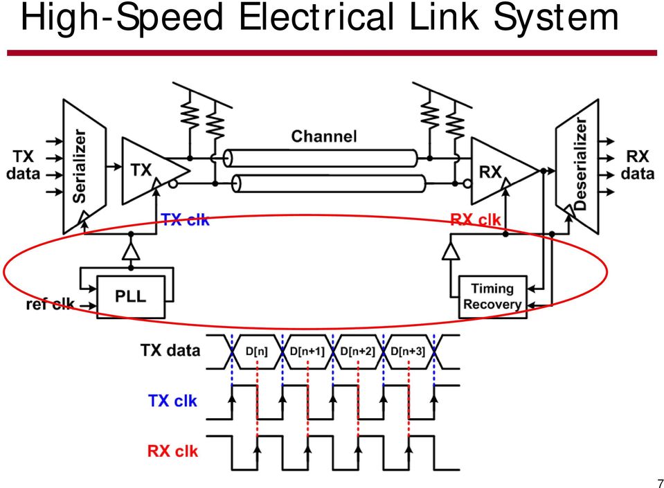
7 High-Speed Electrical Link System 7
8 Clocking Terminology Synchronous Every chip gets same frequency AND phase Used in low-speed busses Mesochronous Same frequency, but unknown phase Requires phase recovery circuitry Can do with or without full CDR Used in fast memories, internal system interfaces, MAC/Packet interfaces Plesiochronous Almost the same frequency, resulting in slowly drifting phase Requires CDR Widely used in high-speed links [Poulton] Asynchronous No clocks at all Request/acknowledge handshake procedure Used in embeddded systems, Unix, Linux 8

9 I/O Clocking Architectures Three basic I/O architectures Common Clock (Synchronous) Forward Clock (Source Synchronous) Embedded Clock (Clock Recovery) These I/O architectures are used for varying applications that require different levels of I/O bandwidth A processor may have one or all of these I/O types Often the same circuitry can be used to emulate different I/O schemes for design reuse 9

10 Common Clock I/O Architecture [Krauter] Common in original computer systems Synchronous system Common bus clock controls chip-to-chip transfers Requires equal length routes to chips to minimize clock skew Data rates typically limited to ~100Mb/s 10

11 Common Clock I/O Cycle Time [Krauter] 11

12 Common Clock I/O Limitations Difficult to control clock skew and propagation delay Need to have tight control of absolute delay to meet a given cycle time Sensitive to delay variations in on-chip circuits and board routes Hard to compensate for delay variations due to low correlation between on-chip and off-chip delays While commonly used in on-chip communication, offers limited speed in I/O applications 12

13 Forward Clock I/O Architecture Common high-speed reference clock is forwarded from TX chip to RX chip Mesochronous system Used in processor-memory interfaces and multi-processor communication Intel QPI Hypertransport Requires one extra clock channel Coherent clocking allows lowto-high frequency jitter tracking Need good clock receive amplifier as the forwarded clock is attenuated by the channel 13

14 Forward Clock I/O Limitations Clock skew can limited forward clock I/O performance Driver strength and loading mismatches Interconnect length mismatches Low pass channel causes jitter amplification Duty-Cycle variations of forwarded clock 14

15 Forward Clock I/O De-Skew Per-channel de-skew allows for significant data rate increases Sample clock adjusted to center clock on the incoming data eye Implementations Delay-Locked Loop and Phase Interpolators Injection-Locked Oscillators Phase Acquisition can be BER based no additional input phase samplers Phase detector based implemented with additional input phase samplers periodically powered on 15

16 Forward Clock I/O Circuits TX PLL TX Clock Distribution Replica TX Clock Driver Channel Forward Clock Amplifier RX Clock Distribution De-Skew Circuit DLL/PI Injection-Locked Oscillator 16

17 Embedded Clock I/O Architecture Can be used in mesochronous or plesiochronous systems Clock frequency and optimum phase position are extracted from incoming data stream Phase detection continuously running CDR Implementations Per-channel PLL-based Dual-loop w/ Global PLL & Local DLL/PI Local Phase-Rotator PLLs 17

18 Embedded Clock I/O Limitations Jitter tracking limited by CDR bandwidth Technology scaling allows CDRs with higher bandwidths which can achieve higher frequency jitter tracking Generally more hardware than forward clock implementations Extra input phase samplers 18

19 Embedded Clock I/O Circuits TX PLL TX Clock Distribution CDR Per-channel PLL-based Dual-loop w/ Global PLL & Local DLL/PI Local Phase-Rotator PLLs Global PLL requires RX clock distribution to individual channels 19

20 Next Time PLL 20

ECEN474: (Analog) VLSI Circuit Design Fall 2010
 VLSI Circuit Design Fall 2010") ECEN474: (Analog) VLSI Circuit Design Fall 2010 Lecture 26: High-Speed I/O Overview Sam Palermo Analog & Mixed-Signal Center Texas A&M University Announcements Project Preliminary report due Nov 19 This
ECEN474: (Analog) VLSI Circuit Design Fall 2010 Lecture 26: High-Speed I/O Overview Sam Palermo Analog & Mixed-Signal Center Texas A&M University Announcements Project Preliminary report due Nov 19 This
Managing High-Speed Clocks
 Managing High-Speed s & Greg Steinke Director, Component Applications Managing High-Speed s Higher System Performance Requires Innovative ing Schemes What Are The Possibilities? High-Speed ing Schemes
PLL DESIGN AND CLOCK/FREQUENCY GENERATION (PLL 设 计 与 时 钟 / 频 率 产 生 ) Woogeun Rhee Institute of Microelectronics Tsinghua University
 Woogeun Rhee Institute of Microelectronics Tsinghua University") PLL DESIGN AND CLOCK/FREQUENCY GENERATION (PLL 设 计 与 时 钟 / 频 率 产 生 ) Woogeun Rhee Institute of Microelectronics Tsinghua University Course Objective This course gives insights into phase-locked clocking
PLL DESIGN AND CLOCK/FREQUENCY GENERATION (PLL 设 计 与 时 钟 / 频 率 产 生 ) Woogeun Rhee Institute of Microelectronics Tsinghua University Course Objective This course gives insights into phase-locked clocking
Lecture 2. High-Speed I/O
 Lecture 2 High-Speed I/O Mark Horowitz Computer Systems Laboratory Stanford University [email protected] Copyright 2007 by Mark Horowitz, with material from Stefanos Sidiropoulos, and Vladimir Stojanovic
8 Gbps CMOS interface for parallel fiber-optic interconnects
 8 Gbps CMOS interface for parallel fiberoptic interconnects Barton Sano, Bindu Madhavan and A. F. J. Levi Department of Electrical Engineering University of Southern California Los Angeles, California
Clocking. Figure by MIT OCW. 6.884 - Spring 2005 2/18/05 L06 Clocks 1
 ing Figure by MIT OCW. 6.884 - Spring 2005 2/18/05 L06 s 1 Why s and Storage Elements? Inputs Combinational Logic Outputs Want to reuse combinational logic from cycle to cycle 6.884 - Spring 2005 2/18/05
A 3.2Gb/s Clock and Data Recovery Circuit Without Reference Clock for a High-Speed Serial Data Link
 A 3.2Gb/s Clock and Data Recovery Circuit Without Reference Clock for a High-Speed Serial Data Link Kang jik Kim, Ki sang Jeong, Seong ik Cho The Department of Electronics Engineering Chonbuk National
Clock Recovery in Serial-Data Systems Ransom Stephens, Ph.D.
 Clock Recovery in Serial-Data Systems Ransom Stephens, Ph.D. Abstract: The definition of a bit period, or unit interval, is much more complicated than it looks. If it were just the reciprocal of the data
Interconnection Networks
 Advanced Computer Architecture (0630561) Lecture 15 Interconnection Networks Prof. Kasim M. Al-Aubidy Computer Eng. Dept. Interconnection Networks: Multiprocessors INs can be classified based on: 1. Mode
White Paper Utilizing Leveling Techniques in DDR3 SDRAM Memory Interfaces
 White Paper Introduction The DDR3 SDRAM memory architectures support higher bandwidths with bus rates of 600 Mbps to 1.6 Gbps (300 to 800 MHz), 1.5V operation for lower power, and higher densities of 2
The Future of Multi-Clock Systems
 NEL FREQUENCY CONTROLS, INC. 357 Beloit Street P.O. Box 457 Burlington,WI 53105-0457 Phone:262/763-3591 FAX:262/763-2881 Web Site: www.nelfc.com Internet: [email protected] The Future of Multi-Clock Systems
Pericom PCI Express 1.0 & PCI Express 2.0 Advanced Clock Solutions
 Pericom PCI Express 1.0 & PCI Express 2.0 Advanced Clock Solutions PCI Express Bus In Today s Market PCI Express, or PCIe, is a relatively new serial pointto-point bus in PCs. It was introduced as an AGP
Jitter in PCIe application on embedded boards with PLL Zero delay Clock buffer
 Jitter in PCIe application on embedded boards with PLL Zero delay Clock buffer Hermann Ruckerbauer EKH - EyeKnowHow 94469 Deggendorf, Germany [email protected] Agenda 1) PCI-Express Clocking
Power Reduction Techniques in the SoC Clock Network. Clock Power
 Power Reduction Techniques in the SoC Network Low Power Design for SoCs ASIC Tutorial SoC.1 Power Why clock power is important/large» Generally the signal with the highest frequency» Typically drives a
Clocks Basics in 10 Minutes or Less. Edgar Pineda Field Applications Engineer Arrow Components Mexico
 Clocks Basics in 10 Minutes or Less Edgar Pineda Field Applications Engineer Arrow Components Mexico Presentation Overview Introduction to Clocks Clock Functions Clock Parameters Common Applications Summary
Design and Modelling of Clock and Data Recovery Integrated Circuit in 130 nm CMOS Technology for 10 Gb/s Serial Data Communications
 Design and Modelling of Clock and Data Recovery Integrated Circuit in 130 nm CMOS Technology for 10 Gb/s Serial Data Communications A THESIS SUBMITTED TO THE DEPARTMENT OF ELECTRONICS AND ELECTRICAL ENGINEERING
Abstract. Cycle Domain Simulator for Phase-Locked Loops
 Abstract Cycle Domain Simulator for Phase-Locked Loops Norman James December 1999 As computers become faster and more complex, clock synthesis becomes critical. Due to the relatively slower bus clocks
PCI-SIG ENGINEERING CHANGE NOTICE
 PCI-SIG ENGINEERING CHANGE NOTICE TITLE: Separate Refclk Independent SSC Architecture (SRIS) DATE: Updated 10 January 013 AFFECTED DOCUMENT: PCI Express Base Spec. Rev. 3.0 SPONSOR: Intel, HP, AMD Part
Sentinel-SSO: Full DDR-Bank Power and Signal Integrity. Design Automation Conference 2014
 Sentinel-SSO: Full DDR-Bank Power and Signal Integrity Design Automation Conference 2014 1 Requirements for I/O DDR SSO Analysis Modeling Package and board I/O circuit and layout PI + SI feedback Tool
Chapter 6 PLL and Clock Generator
 Chapter 6 PLL and Clock Generator The DSP56300 core features a Phase Locked Loop (PLL) clock generator in its central processing module. The PLL allows the processor to operate at a high internal clock
Any-Rate Precision Clocks
 Any-Rate Precision Clocks Wireline Market Overview Analog Modems Large installed base and growth in embedded applications Voice Transition to VoIP to reduce service provider cost-of-ownership Timing Large,
Alpha CPU and Clock Design Evolution
 Alpha CPU and Clock Design Evolution This lecture uses two papers that discuss the evolution of the Alpha CPU and clocking strategy over three CPU generations Gronowski, Paul E., et.al., High Performance
DS2187 Receive Line Interface
 Receive Line Interface www.dalsemi.com FEATURES Line interface for T1 (1.544 MHz) and CEPT (2.048 MHz) primary rate networks Extracts clock and data from twisted pair or coax Meets requirements of PUB
Explore Efficient Test Approaches for PCIe at 16GT/s Kalev Sepp Principal Engineer Tektronix, Inc
 Explore Efficient Test Approaches for PCIe at 16GT/s Kalev Sepp Principal Engineer Tektronix, Inc Copyright 2015, PCI-SIG, All Rights Reserved 1 Disclaimer Presentation Disclaimer: All opinions, judgments,
How To Test The Performance Of An Oversampling Cdr In An Fgpa, Jitter And Memory On A Black Box (Cdr) In A Test Program
 In A Test Program") 74 M. KUBÍČEK, Z. KOLKA, BLIND OVERSAMPLING DATA RECOVERY WITH LOW HARDWARE COMPLEXITY Blind Oversampling Data Recovery with Low Hardware Complexity Michal KUBÍČEK, Zdeněk KOLKA Dept. of Radio Electronics,
74 M. KUBÍČEK, Z. KOLKA, BLIND OVERSAMPLING DATA RECOVERY WITH LOW HARDWARE COMPLEXITY Blind Oversampling Data Recovery with Low Hardware Complexity Michal KUBÍČEK, Zdeněk KOLKA Dept. of Radio Electronics,
Analysis and Design of Robust Multi-Gb/s Clock and Data Recovery Circuits
 Analysis and Design of Robust Multi-Gb/s Clock and Data Recovery Circuits by David J. Rennie A thesis presented to the University of Waterloo in fulfillment of the thesis requirement for the degree of
EEM870 Embedded System and Experiment Lecture 1: SoC Design Overview
 EEM870 Embedded System and Experiment Lecture 1: SoC Design Overview Wen-Yen Lin, Ph.D. Department of Electrical Engineering Chang Gung University Email: [email protected] Feb. 2013 Course Overview
Jitter Transfer Functions in Minutes
 Jitter Transfer Functions in Minutes In this paper, we use the SV1C Personalized SerDes Tester to rapidly develop and execute PLL Jitter transfer function measurements. We leverage the integrated nature
Loop Bandwidth and Clock Data Recovery (CDR) in Oscilloscope Measurements. Application Note 1304-6
 in Oscilloscope Measurements. Application Note 1304-6") Loop Bandwidth and Clock Data Recovery (CDR) in Oscilloscope Measurements Application Note 1304-6 Abstract Time domain measurements are only as accurate as the trigger signal used to acquire them. Often
Loop Bandwidth and Clock Data Recovery (CDR) in Oscilloscope Measurements Application Note 1304-6 Abstract Time domain measurements are only as accurate as the trigger signal used to acquire them. Often
AN ESTIMATION APPROACH TO CLOCK AND DATA RECOVERY
 AN ESTIMATION APPROACH TO CLOCK AND DATA RECOVERY A DISSERTATION SUBMITTED TO THE DEPARTMENT OF ELECTRICAL ENGINEERING AND THE COMMITTEE ON GRADUATE STUDIES OF STANFORD UNIVERSITY IN PARTIAL FULFILLMENT
Phase-Locked Loop Based Clock Generators
 Phase-Locked Loop Based Clock Generators INTRODUCTION As system clock frequencies reach 100 MHz and beyond maintaining control over clock becomes very important In addition to generating the various clocks
Continuous-Time Converter Architectures for Integrated Audio Processors: By Brian Trotter, Cirrus Logic, Inc. September 2008
 Continuous-Time Converter Architectures for Integrated Audio Processors: By Brian Trotter, Cirrus Logic, Inc. September 2008 As consumer electronics devices continue to both decrease in size and increase
Calibration Techniques for High- Bandwidth Source-Synchronous Interfaces
 DesignCon 2007 Calibration Techniques for High- Bandwidth Source-Synchronous Interfaces Manoj Roge, Altera Corporation Andy Bellis, Altera Corporation Phil Clarke, Altera Corporation Joseph Huang, Altera
Clocking. Clocking in the Digital Network
 Clocking Clocking in the Digital Network Stratum Levels Clocking Distribution Single Point versus Multiple Points Timing Differences Correcting Timing Errors Buffers 1 Clocking The most important aspect
MULTI-GIGABIT per second (Gbps) serial binary links
 serial binary links") IEEE JOURNAL OF SOLID-STATE CIRCUITS, VOL. 41, NO. 8, AUGUST 2006 1867 A Digital Clock and Data Recovery Architecture for Multi-Gigabit/s Binary Links Jeff L. Sonntag and John Stonick, Member, IEEE Abstract
IEEE JOURNAL OF SOLID-STATE CIRCUITS, VOL. 41, NO. 8, AUGUST 2006 1867 A Digital Clock and Data Recovery Architecture for Multi-Gigabit/s Binary Links Jeff L. Sonntag and John Stonick, Member, IEEE Abstract
Digital Signal Controller Based Automatic Transfer Switch
 Digital Signal Controller Based Automatic Transfer Switch by Venkat Anant Senior Staff Applications Engineer Freescale Semiconductor, Inc. Abstract: An automatic transfer switch (ATS) enables backup generators,
USB Audio Simplified
 USB Audio Simplified The rapid expansion of the universal serial bus (USB) standard in consumer electronics products has extended the use of USB connectivity to propagate and control digital audio. USB
AMD Opteron Quad-Core
 AMD Opteron Quad-Core a brief overview Daniele Magliozzi Politecnico di Milano Opteron Memory Architecture native quad-core design (four cores on a single die for more efficient data sharing) enhanced
Lizy Kurian John Electrical and Computer Engineering Department, The University of Texas as Austin
 BUS ARCHITECTURES Lizy Kurian John Electrical and Computer Engineering Department, The University of Texas as Austin Keywords: Bus standards, PCI bus, ISA bus, Bus protocols, Serial Buses, USB, IEEE 1394
High-Speed Electronics
 High-Speed Electronics Mentor User Conference 2005 - München Dr. Alex Huber, [email protected] Zentrum für Mikroelektronik Aargau, 5210 Windisch, Switzerland www.zma.ch Page 1 Outline 1. Motivation 2. Speed
PowerPC Microprocessor Clock Modes
 nc. Freescale Semiconductor AN1269 (Freescale Order Number) 1/96 Application Note PowerPC Microprocessor Clock Modes The PowerPC microprocessors offer customers numerous clocking options. An internal phase-lock
1+1 PROTECTION WITHOUT RELAYS USING IDT82V2044/48/48L & IDT82V2054/58/58L HITLESS PROTECTION SWITCHING
 1+1 PROTECTION WITHOUT RELAYS USING IDT82V2044/48/48L & IDT82V2054/58/58L APPLICATION NOTE AN-357 1.0 INTRODUCTION In today's highly competitive market, high quality of service, QOS, and reliability is
USB 3.0 CDR Model White Paper Revision 0.5
 USB 3.0 CDR Model White Paper Revision 0.5 January 15, 2009 INTELLECTUAL PROPERTY DISCLAIMER THIS WHITE PAPER IS PROVIDED TO YOU AS IS WITH NO WARRANTIES WHATSOEVER, INCLUDING ANY WARRANTY OF MERCHANTABILITY,
Keysight Technologies Forward Clocking - Receiver (RX) Jitter Tolerance Test with J-BERT N4903B High-Performance Serial BERT.
 Jitter Tolerance Test with J-BERT N4903B High-Performance Serial BERT.") Keysight Technologies Forward Clocking - Receiver (RX) Jitter Tolerance Test with J-BERT N4903B High-Performance Serial BERT Application Note Introduction J-BERT N4903B highperformance serial BERT with
Keysight Technologies Forward Clocking - Receiver (RX) Jitter Tolerance Test with J-BERT N4903B High-Performance Serial BERT Application Note Introduction J-BERT N4903B highperformance serial BERT with
ISSCC 2003 / SESSION 4 / CLOCK RECOVERY AND BACKPLANE TRANSCEIVERS / PAPER 4.7
 ISSCC 2003 / SESSION 4 / CLOCK RECOVERY AND BACKPLANE TRANSCEIVERS / PAPER 4.7 4.7 A 2.7 Gb/s CDMA-Interconnect Transceiver Chip Set with Multi-Level Signal Data Recovery for Re-configurable VLSI Systems
Selecting the Optimum PCI Express Clock Source
 Selecting the Optimum PCI Express Clock Source PCI Express () is a serial point-to-point interconnect standard developed by the Component Interconnect Special Interest Group (PCI-SIG). lthough originally
Fairchild Solutions for 133MHz Buffered Memory Modules
 AN-5009 Fairchild Semiconductor Application Note April 1999 Revised December 2000 Fairchild Solutions for 133MHz Buffered Memory Modules Fairchild Semiconductor provides several products that are compatible
INF4420 Introduction
 INF4420 Introduction Spring 2012 Jørgen Andreas Michaelsen ([email protected]) Outline Practical information about the course. Context (placing what we will learn in a larger context) Outline of the
An All-Digital Phase-Locked Loop with High Resolution for Local On-Chip Clock Synthesis
 An All-Digital Phase-Locked Loop with High Resolution for Local On-Chip Clock Synthesis Oliver Schrape 1, Frank Winkler 2, Steffen Zeidler 1, Markus Petri 1, Eckhard Grass 1, Ulrich Jagdhold 1 International
PCI Technology Overview
 PCI Technology Overview February 2003 February 2003 Page 1 Agenda History and Industry Involvement Technology Information Conventional PCI PCI-X 1.0 2.0 PCI Express Other Digi Products in PCI/PCI-X environments
Simplifying System Design Using the CS4350 PLL DAC
 Simplifying System Design Using the CS4350 PLL 1. INTRODUCTION Typical Digital to Analog Converters (s) require a high-speed Master Clock to clock their digital filters and modulators, as well as some
Making Multicore Work and Measuring its Benefits. Markus Levy, president EEMBC and Multicore Association
 Making Multicore Work and Measuring its Benefits Markus Levy, president EEMBC and Multicore Association Agenda Why Multicore? Standards and issues in the multicore community What is Multicore Association?
ICS379. Quad PLL with VCXO Quick Turn Clock. Description. Features. Block Diagram
 Quad PLL with VCXO Quick Turn Clock Description The ICS379 QTClock TM generates up to 9 high quality, high frequency clock outputs including a reference from a low frequency pullable crystal. It is designed
Agenda. Michele Taliercio, Il circuito Integrato, Novembre 2001
 Agenda Introduzione Il mercato Dal circuito integrato al System on a Chip (SoC) La progettazione di un SoC La tecnologia Una fabbrica di circuiti integrati 28 How to handle complexity G The engineering
Outline. Introduction. Multiprocessor Systems on Chip. A MPSoC Example: Nexperia DVP. A New Paradigm: Network on Chip
 Outline Modeling, simulation and optimization of Multi-Processor SoCs (MPSoCs) Università of Verona Dipartimento di Informatica MPSoCs: Multi-Processor Systems on Chip A simulation platform for a MPSoC
SDI SDI SDI. Frame Synchronizer. Figure 1. Typical Example of a Professional Broadcast Video
 TIMING AND SYNCHRONIZATION IN BROADCAST VIDEO 1. Introduction Digitization of video signals has been common practice in broadcast video for many years. Early digital video was commonly encoded on a -bit
Fondamenti su strumenti di sviluppo per microcontrollori PIC
 Fondamenti su strumenti di sviluppo per microcontrollori PIC MPSIM ICE 2000 ICD 2 REAL ICE PICSTART Ad uso interno del corso Elettronica e Telecomunicazioni 1 2 MPLAB SIM /1 MPLAB SIM is a discrete-event
BURST-MODE communication relies on very fast acquisition
 IEEE TRANSACTIONS ON CIRCUITS AND SYSTEMS II: EXPRESS BRIEFS, VOL. 52, NO. 8, AUGUST 2005 437 Instantaneous Clockless Data Recovery and Demultiplexing Behnam Analui and Ali Hajimiri Abstract An alternative
Serial Communications
 Serial Communications 1 Serial Communication Introduction Serial communication buses Asynchronous and synchronous communication UART block diagram UART clock requirements Programming the UARTs Operation
11. High-Speed Differential Interfaces in Cyclone II Devices
 11. High-Speed Differential Interfaces in Cyclone II Devices CII51011-2.2 Introduction From high-speed backplane applications to high-end switch boxes, low-voltage differential signaling (LVDS) is the
Table 1 SDR to DDR Quick Reference
 TECHNICAL NOTE TN-6-05 GENERAL DDR SDRAM FUNCTIONALITY INTRODUCTION The migration from single rate synchronous DRAM (SDR) to double rate synchronous DRAM (DDR) memory is upon us. Although there are many
IN RECENT YEARS, the increase of data transmission over
 1356 IEEE JOURNAL OF SOLID-STATE CIRCUITS, VOL. 39, NO. 8, AUGUST 2004 A 3.125-Gb/s Clock and Data Recovery Circuit for the 10-Gbase-LX4 Ethernet Rong-Jyi Yang, Student Member, IEEE, Shang-Ping Chen, and
FURTHER READING: As a preview for further reading, the following reference has been provided from the pages of the book below:
 FURTHER READING: As a preview for further reading, the following reference has been provided from the pages of the book below: Title: Broadband Telecommunications Handbook Author: Regis J. Bud Bates Publisher:
PAC52XX Clock Control Firmware Design
 APPLICATION NOTE PAC52XX Clock Control Firmware Design TM Marc Sousa Senior Manager, Systems and Firmware www.active-semi.com Copyright 2014 Active-Semi, Inc. TABLE OF CONTENTS APPLICATION NOTE... 1 Table
W a d i a D i g i t a l
 Wadia Decoding Computer Overview A Definition What is a Decoding Computer? The Wadia Decoding Computer is a small form factor digital-to-analog converter with digital pre-amplifier capabilities. It is
Am186ER/Am188ER AMD Continues 16-bit Innovation
 Am186ER/Am188ER AMD Continues 16-bit Innovation 386-Class Performance, Enhanced System Integration, and Built-in SRAM Problem with External RAM All embedded systems require RAM Low density SRAM moving
LatticeECP3 High-Speed I/O Interface
 April 2013 Introduction Technical Note TN1180 LatticeECP3 devices support high-speed I/O interfaces, including Double Data Rate (DDR) and Single Data Rate (SDR) interfaces, using the logic built into the
Principles and characteristics of distributed systems and environments
 Principles and characteristics of distributed systems and environments Definition of a distributed system Distributed system is a collection of independent computers that appears to its users as a single
Glitch Free Frequency Shifting Simplifies Timing Design in Consumer Applications
 Glitch Free Frequency Shifting Simplifies Timing Design in Consumer Applications System designers face significant design challenges in developing solutions to meet increasingly stringent performance and
Progress Record. Course 21 (V) Associate of Applied Science in Computer Information Technology and Systems Management
 Associate of Applied Science in Computer Information Technology and Systems Management") Progress Record Study your lessons in the order listed below. As graded examinations are returned to you, enter your grade in the space below. Set a schedule for yourself then watch your progress. Course
Progress Record Study your lessons in the order listed below. As graded examinations are returned to you, enter your grade in the space below. Set a schedule for yourself then watch your progress. Course
PCI Express: The Evolution to 8.0 GT/s. Navraj Nandra, Director of Marketing Mixed-Signal and Analog IP, Synopsys
 PCI Express: The Evolution to 8.0 GT/s Navraj Nandra, Director of Marketing Mixed-Signal and Analog IP, Synopsys PCIe Enterprise Computing Market Transition From Gen2 to Gen3 Total PCIe instances. 2009
2.1 CAN Bit Structure The Nominal Bit Rate of the network is uniform throughout the network and is given by:
 Order this document by /D CAN Bit Timing Requirements by Stuart Robb East Kilbride, Scotland. 1 Introduction 2 CAN Bit Timing Overview The Controller Area Network (CAN) is a serial, asynchronous, multi-master
Chapter 2. Multiprocessors Interconnection Networks
 Chapter 2 Multiprocessors Interconnection Networks 2.1 Taxonomy Interconnection Network Static Dynamic 1-D 2-D HC Bus-based Switch-based Single Multiple SS MS Crossbar 2.2 Bus-Based Dynamic Single Bus
INPUT/OUTPUT ORGANIZATION
 INPUT/OUTPUT ORGANIZATION Accessing I/O Devices I/O interface Input/output mechanism Memory-mapped I/O Programmed I/O Interrupts Direct Memory Access Buses Synchronous Bus Asynchronous Bus I/O in CO and
Timing Errors and Jitter
 Timing Errors and Jitter Background Mike Story In a sampled (digital) system, samples have to be accurate in level and time. The digital system uses the two bits of information the signal was this big
Infrastructure Matters: POWER8 vs. Xeon x86
 Advisory Infrastructure Matters: POWER8 vs. Xeon x86 Executive Summary This report compares IBM s new POWER8-based scale-out Power System to Intel E5 v2 x86- based scale-out systems. A follow-on report
High speed pattern streaming system based on AXIe s PCIe connectivity and synchronization mechanism
 High speed pattern streaming system based on AXIe s connectivity and synchronization mechanism By Hank Lin, Product Manager of ADLINK Technology, Inc. E-Beam (Electron Beam) lithography is a next-generation
FPGA Clocking. Clock related issues: distribution generation (frequency synthesis) multiplexing run time programming domain crossing
 multiplexing run time programming domain crossing") FPGA Clocking Clock related issues: distribution generation (frequency synthesis) Deskew multiplexing run time programming domain crossing Clock related constraints 100 Clock Distribution Device split
FPGA Clocking Clock related issues: distribution generation (frequency synthesis) Deskew multiplexing run time programming domain crossing Clock related constraints 100 Clock Distribution Device split
A 10GB/S FULL ON-CHIP BANG-BANG CLOCK AND DATA RECOVERY SYSTEM USING AN ADAPTIVE LOOP BANDWIDTH STRATEGY. A Thesis HYUNG-JOON JEON
 A 10GB/S FULL ON-CHIP BANG-BANG CLOCK AND DATA RECOVERY SYSTEM USING AN ADAPTIVE LOOP BANDWIDTH STRATEGY A Thesis by HYUNG-JOON JEON Submitted to the Office of Graduate Studies of Texas A&M University
Using the On-Chip Signal Quality Monitoring Circuitry (EyeQ) Feature in Stratix IV Transceivers
 Feature in Stratix IV Transceivers") Using the On-Chip Signal Quality Monitoring Circuitry (EyeQ) Feature in Stratix IV Transceivers AN-605-1.2 Application Note This application note describes how to use the on-chip signal quality monitoring
Using the On-Chip Signal Quality Monitoring Circuitry (EyeQ) Feature in Stratix IV Transceivers AN-605-1.2 Application Note This application note describes how to use the on-chip signal quality monitoring
A 1.62/2.7/5.4 Gbps Clock and Data Recovery Circuit for DisplayPort 1.2 with a single VCO
 JOURNAL OF SEMICONDUCTOR TECHNOLOGY AND SCIENCE, VOL.13, NO.3, JUNE, 2013 http://dx.doi.org/10.5573/jsts.2013.13.3.185 A 1.62/2.7/5.4 Clock and Data Recovery Circuit for DisplayPort 1.2 with a single VCO
Digitale Signalverarbeitung mit FPGA (DSF) Soft Core Prozessor NIOS II Stand Mai 2007. Jens Onno Krah
 Soft Core Prozessor NIOS II Stand Mai 2007. Jens Onno Krah") (DSF) Soft Core Prozessor NIOS II Stand Mai 2007 Jens Onno Krah Cologne University of Applied Sciences www.fh-koeln.de [email protected] NIOS II 1 1 What is Nios II? Altera s Second Generation
(DSF) Soft Core Prozessor NIOS II Stand Mai 2007 Jens Onno Krah Cologne University of Applied Sciences www.fh-koeln.de [email protected] NIOS II 1 1 What is Nios II? Altera s Second Generation
How to design and implement firmware for embedded systems
 How to design and implement firmware for embedded systems Last changes: 17.06.2010 Author: Rico Möckel The very beginning: What should I avoid when implementing firmware for embedded systems? Writing code
Programmable Logic Design Grzegorz Budzyń Lecture. 10: FPGA clocking schemes
 Programmable Logic Design Grzegorz Budzyń Lecture 10: FPGA clocking schemes Plan Introduction Definitions Clockskew Metastability FPGA clocking resources DCM PLL Introduction One of the most important
Course 12 Synchronous transmission multiplexing systems used in digital telephone networks
 Course 12 Synchronous transmission multiplexing systems used in digital telephone networks o Disadvantages of the PDH transmission multiplexing system PDH: no unitary international standardization of the
Title: Low EMI Spread Spectrum Clock Oscillators
 Title: Low EMI oscillators Date: March 3, 24 TN No.: TN-2 Page 1 of 1 Background Title: Low EMI Spread Spectrum Clock Oscillators Traditional ways of dealing with EMI (Electronic Magnetic Interference)
Lecture 18: Interconnection Networks. CMU 15-418: Parallel Computer Architecture and Programming (Spring 2012)
") Lecture 18: Interconnection Networks CMU 15-418: Parallel Computer Architecture and Programming (Spring 2012) Announcements Project deadlines: - Mon, April 2: project proposal: 1-2 page writeup - Fri,
Lecture 18: Interconnection Networks CMU 15-418: Parallel Computer Architecture and Programming (Spring 2012) Announcements Project deadlines: - Mon, April 2: project proposal: 1-2 page writeup - Fri,
Multipath fading in wireless sensor mote
 Multipath fading in wireless sensor mote Vaishali M.Tech (VLSI), IMSEC, Ghaziabad/MTU, Noida Abstract: In this paper we study about the new technology as to transfer the data with the help of smart device,
TIMING-DRIVEN PHYSICAL DESIGN FOR DIGITAL SYNCHRONOUS VLSI CIRCUITS USING RESONANT CLOCKING
 TIMING-DRIVEN PHYSICAL DESIGN FOR DIGITAL SYNCHRONOUS VLSI CIRCUITS USING RESONANT CLOCKING BARIS TASKIN, JOHN WOOD, IVAN S. KOURTEV February 28, 2005 Research Objective Objective: Electronic design automation
AMS Verification at SoC Level: A practical approach for using VAMS vs SPICE views
 AMS Verification at SoC Level: A practical approach for using VAMS vs SPICE views Nitin Pant, Gautham Harinarayan, Manmohan Rana Accellera Systems Initiative 1 Agenda Need for SoC AMS Verification Mixed
Equalization for High-Speed Serial Interfaces in Xilinx 7 Series FPGA Transceivers
 White Paper: 7 Series FPGAs WP419 (v1.0) March 27, 2012 Equalization for High-Speed Serial Interfaces in Xilinx 7 Series FPGA Transceivers By: Harry Fu The appetite for data is exploding, and the industry
Jitter Budget for 10 Gigabit Ethernet Applications with SiTime SiT9120/1 Oscillators
 February 2014 Jitter Budget for 10 Gigabit Ethernet Applications with SiTime SiT9120/1 Oscillators 1 Introduction The 10 Gigabit Ethernet (10GbE) specifications are defined in clauses 44 through 54 of
Learning Outcomes. Simple CPU Operation and Buses. Composition of a CPU. A simple CPU design
 Learning Outcomes Simple CPU Operation and Buses Dr Eddie Edwards [email protected] At the end of this lecture you will Understand how a CPU might be put together Be able to name the basic components
Rong-Jyi YANG, Nonmember and Shen-Iuan LIU a), Member
, Member") 1726 PAPER Special Section on Papers Selected from AP-ASIC 2004 A Fully Integrated 1.7 3.125 Gbps Clock and Data Recovery Circuit Using a Gated Frequency Detector Rong-Jyi YANG, Nonmember and Shen-Iuan
1726 PAPER Special Section on Papers Selected from AP-ASIC 2004 A Fully Integrated 1.7 3.125 Gbps Clock and Data Recovery Circuit Using a Gated Frequency Detector Rong-Jyi YANG, Nonmember and Shen-Iuan
Clocking Solutions. Wired Communications / Networking Wireless Communications Industrial Automotive Consumer Computing. ti.
 ing Solutions Wired Communications / Networking Wireless Communications Industrial Automotive Consumer Computing ti.com/clocks 2014 Accelerate Time-to-Market with Easy-to-Use ing Solutions Texas Instruments