Chapter 7 Memory and Programmable Logic
|
|
|
- Terence Ramsey
- 8 years ago
- Views:
Transcription
1 NCNU_2013_DD_7_1 Chapter 7 Memory and Programmable Logic 71I 7.1 Introduction ti 7.2 Random Access Memory 7.3 Memory Decoding 7.5 Read Only Memory 7.6 Programmable Logic Array 77P 7.7 Programmable Array Logic 7.8 Sequential Programmable Devices

2 7-1 Introduction NCNU_2013_DD_7_2 Memories are for binary information storage. Two main memory types: random access memory (RAM) and read only memory (ROM). [actually both of them are random accessible] RAM can perform both write and read operations, while ROM can perform only the read operation. Wit Write: storing new information into memory Read: transferring the stored information out of memory ROM is a programmable logic device (PLD) which stores the binary information via a hardware programming process. A PLD is an IC with internal logic gates connected through electronic paths that behave similarly il l to fuses that t will be burned out to obtain a specified function. Programmable logic array (PLA), programmable array logic (PAL), and the field programmable gate array y( (FPGA) are other commonly seen PLDs.

3 7-2 Random-Access Memory NCNU_2013_DD_7_3 A memory unit includes an array of storage cells, together th with associated read/write control circuits. The architecture of memory is such that information can be selectively retrieved from any of its internal locations. A memory unit stores binary information in groups of bits called words that move in and out of storage as a unit. A memory word is a group of 1 s and 0 s and may represent a number, an instruction, one or more alphanumeric characters, or any other binary coded information. Most computer memory uses words that are multiples of 8 bits in length. The capacity of a memory unit is usually stated t as the total t number of bytes that t the unit can store.

4 A Memory Unit of RAM NCNU_2013_DD_7_4 Memory is accessed dthrough hdata input and output tlines, address selection lines, and control lines that specify the direction of transfer. The n data input lines provide the information to be stored in memory, and the n data output lines supply the information coming out of memory. The k address lines specify the particular word chosen. Read/Write are the control linputs specify the transfer direction. i Each word in memory is assigned an identification address ranging from 0 up to 2 k - 1. The number of words (or bytes) in memory is typically ( y ) y yp y with one of the letters K (kilo), M (mega), and G (giga).

5 Example: 1K x 16 Memory A Memory NCNU_2013_DD_7_5

6 Write and Read Operations Wit Write operation Apply the binary address to the address lines Apply the data bits to the data input lines Activate the write input NCNU_2013_DD_7_6 Read operation Apply the binary address to the address lines Activate the read input Read/Write share a same pin; when memory is enabled, 0 for read and 1 for write.

7 RAM in HDL NCNU_2013_DD_7_7

8 Timing Waveforms NCNU_2013_DD_7_8 The memory operation is controlled by an external device such as a central processing unit (CPU) which is usually synchronized by a clock. Instead, the memory s read and write operations are specified by control inputs. The access time of memory is the time required to select a word and read it. The cycle time of memory is the time required to complete a write operation. The CPU must provide the memory control signals to synchronize its internal clocked operations with the read and write operations. This means that the access time and cycle time of the memory must be within a time equal to a fixed number of CPU clock cycles.

9 Write Cycle CPU clock is 50 MHz; a period of 20 ns The access/cycle time < 50 ns NCNU_2013_DD_7_9

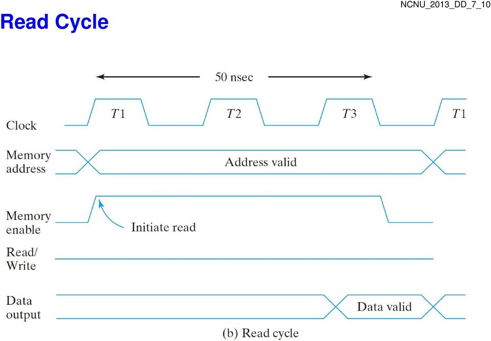
10 Read Cycle NCNU_2013_DD_7_10
11 Types of Memories Staticti information are stored in latches remains valid as long as power is applied short read/write cycle Dynamic information are stored in the form of charges on capacitors the stored charge tends to discharge with time need to be refreshed (read and write back) reduced power consumption larger memory capacity NCNU_2013_DD_7_11 Volatile lose stored information when power is turned off SRAM, DRAM Non-volatile retain stored information after the removal of power ROM EPROM, EEPROM Flash memory

12 7-3 Memory Decoding NCNU_2013_DD_7_12 A memory unit contains memory cells and ddecoding di circuits. it Decoding circuits may select the memory word specified by the input address. A bit memory cell is shown below: The cell is modeled by an SR latch with associated gates to form a D latch. Actually, the cell is an electronic circuit with four to six transistors. The cell must be very small in order to be able to pack as many cells as possible i h ll il bl i IC hi Thi k b 10 9 ll d i 1 2 in the small area available in an IC chip. Think about 10 9 cells crowed in 1 cm 2.

13 A 4 x 4 RAM NCNU_2013_DD_7_13

14 NCNU_2013_DD_7_14 Two address lines are needed dto go through ha 2 x 4 decoder d to select one of fthe four words. The decoder is enabled with the memory enable input. Once a word has been selected (addressed), the read/write input determines the operation. During the read operation, the four bits of the selected word go through hthe multiinput OR gates to the output terminals. During the write operation, the data available in the input lines are transferred into the four binary cells of the selected word. Commercial RAMs may have a capacity of millions to trillions of words, and each word may range from 1 to 64bits. A memory with 2k words of n bits per word requires k address lines that go into a k x 2 k decoder. Each one of the decoder outputs selects one word of n bits for reading or writing. A decoder with k inputs and 2 k outputs requires 2 k AND gates with k inputs per gate.

15 Coincident Decoding NCNU_2013_DD_7_15 At two-dimensional i selection scheme can reduce the complexity of the decoding di circuits; for example, 1-k memory is shown. Each intersection represents a word that may have any number of bits. A single 10 x 1024 decoder needs input AND gates. Two 5 x 32 decoders require only 64 5-input AND gates. Reduce the circuit complexity and the cycle time. which address?

16 Address Multiplexing NCNU_2013_DD_7_16 Address multiplexing l i is used in DRAM design to reduce the number of pins in IC package. In a two dimensional array, the address is applied in two parts at different times, with the row address first and the column address second. Addresses are respectively latched into the 8-bit registers. RAS: row address strobe CAS: column address strobe The timing is important in the design and utilization of RAM.

17 7-5 Read-Only Memory (ROM) NCNU_2013_DD_7_17 ROM stores binary information permanently even when power is turned off and on again. A block diagram of a ROM consisting of k inputs and n outputs is shown. k address input lines can specify 2 k words. The inputs provide the address, and the outputs give the data word selected by the address. Integrated circuit ROM chips have one or more enable inputs and sometimes come with three state outputs to facilitate the construction of large ROM arrays.

18 Example: 32 x 8 ROM 5 t 32 d d 5-to-32 decoder 8 OR gates each has 32 inputs 32 x 8 internal programmable connections NCNU_2013_DD_7_18

19 Programming ROM Af fused-switch in each cross-point: itclose (two lines are connected) td) or open The fuse that can be blown by applying a high voltage pulse. NCNU_2013_DD_7_19 x: connected what are stored in these words? see next slide

20 ROM Table NCNU_2013_DD_7_20

21 Combinational Circuit Implementation ROM: a decoder d + OR gates sum of minterms a Boolean function => sum of minterms for an n-input, m-output combinational circuit 2 n m ROM the decoder is fixed, the inputs to OR gate is programmable Design procedure: 1. determine the size of ROM 2. obtain the programming truth table of the ROM 3. the truth th table = the fuse pattern NCNU_2013_DD_7_21
22 Example 7-1 NCNU_2013_DD_7_22 Design a combinational circuit it using a ROM. The circuit it accepts a three bit number and outputs a binary number equal to the square of the input number. 3 inputs and 6 outputs are required A partial truth table for the ROM B 1 = 0 B 0 = A 0 so, 8 x 4 ROM is enough
23 ROM Implementation for Example 7.1 NCNU_2013_DD_7_23 ROM table
24 Types of ROM Mask programming ROM IC manufacturers is economical only if large quantities PROM: Programmable ROM fuses, one-time programmable (OTP) universal programmer EPROM: Erasable PROM floating gate (tunneling) ultraviolet l t light erasable with transparent t window EEPROM: Electrically Erasable PROM longer time is needed to write in system programmable (ISP) Flash memory allowing simultaneous erasing of blocks of memory (flash erasable) current mainstream product NAND type and NOR type very high h density High voltage (> 10V) is required for non-mask programming NCNU_2013_DD_7_24
25 Combinational PLDs Th j t f bi ti l PLD diff i i th l t f th Three major types of combinational PLDs, differing in the placement of the programmable connections in the AND OR array. NCNU_2013_DD_7_25
26 7.6 Programmable Logic Array (PLA) NCNU_2013_DD_7_26 An array of programmable AND gates can generate any product tterms of fthe inputs; and an array of programmable OR gates can generate the sums of the products. More flexible use less circuits than ROM. Example: 3 inputs 4 product terms 2 outputs t XOR for inverting F 1 = AB + AC + A BC F 2 = (AC + BC)
27 PLA Programming Table NCNU_2013_DD_7_27 F 1 = AB + AC + A BC F 2 = (AC + BC) The size of a PLA is specified by the number of inputs, the number of product terms, and the number of outputs. For n inputs, k product terms, and m outputs, the internal logic of the PLA consists of n buffer inverter gates, k AND gates, m OR gates, and m XOR gates. There are 2n x k connections between the inputs and the AND array, k x m connections between the AND and OR arrays, y, and m connections associated with the XOR gates.
28 Examples 7-2 NCNU_2013_DD_7_28 Use PLA to implement tf F 1 (A, B, C) = (0124)F (0, 1, 2, 4); F 2 (A, B, C) = (0567) (0, 5, 6, Both the true value and the complement of the function should be simplified to check to reduce the number of distinct product terms (AND gates needed). The number of literals in a term is not important in PLA design The K-map for the simplification F 1 = (AB + AC + BC) F 2 = AB + AC + A B C Only four distinct product terms: AB, AC, BC, and A B C.
29 NCNU_2013_DD_7_29 AB AC BC A B C
30 7-7 Programmable Array Logic (PAL) PAL has a fixed OR array and a programmable AND array. Easier to program than, but is not as flexible as, the PLA. Example: PAL with 4 inputs and 4 outputs. There are four sections of three wide AND OR array, i.e. there are three programmable AND gates in each section and one fixed OR gate. The Boolean functions must be simplified to fit into each section. One of fthe outputs t is fed back kinto the AND gates for implementing functions with a large number of product terms. Unlike PLA, a product term cannot be shared among two or more OR gates; therefore, each function can be simplified by itself. NCNU_2013_DD_7_30
31 An Example Implementation Ui Using a PALt to design the following fll Boolean functions w(a,b,c,d) = (2,12,13) x(a,b,c,d) = ( ) (7,8,9,10,11,12,13,14) y(a,b,c,d) = (0,2,3,4,5,6,7,8,10,11,15) z(a,b,c,d) = (1,2,8,12,13) Simplify the functions w = ABC + A B CD x = A + BCD y = A B + CD + B D z = ABC + A B CD + AC D + A B C D = w + AC D + A B C D z has four product terms and can be reduced by using w. NCNU_2013_DD_7_31
32 PAL Programming Table NCNU_2013_DD_7_32
33 NCNU_2013_DD_7_33 w = ABC + A B CD x = A + BCD y = A B +CD+B D + z = w + AC D + A B C D
34 7-8 Sequential Programmable Devices Sequential programmable devices include both gates and dflip flops. Three major types: 1. Sequential (or simple) programmable logic device (SPLD) 2. Complex programmable logic device (CPLD) 3. Field programmable gate array (FPGA) NCNU_2013_DD_7_34
35 SPLD and its Macrocell NCNU_2013_DD_7_35 The sequential PLD is sometimes referred to as a simple PLD to differentiate t it from the complex PLD. A PAL that includes flip flops p is referred to as a registered PAL. Each section of an SPLD is called a macrocell, which is a circuit that contains a sum of products combinational logic function and an optional flip flop. Ab basic macrocell: PAL + edge-triggered dd-ff + tri-state output
36 Complex PLD NCNU_2013_DD_7_36 CPLD, which h is a collection of individual id PLDs on a single IC, is more economical to use than SPLD. A programmable interconnection structure (switch matrix) allows the PLDs to be connected to each other. The input output (I/O) blocks provide the connections to the IC pins which are driven by a three state buffer and can be programmed to act as input or output.
37 Field-Programmable Gate Array (FPGA) NCNU_2013_DD_7_37 Gate array is an IC design methodology with several lhundred dthousand gates (transistors) fabricated in a single chip while their interconnections are determined from the designer s specification in the last steps of foundry service. A field programmable gate array (FPGA) is a gate array like IC chip that can be programmed at the user s location. A typical FPGA consists of an array of millions of logic blocks (lookup tables, multiplexers, gates, and flip flops), surrounded by programmable input and output blocks and connected together via programmable interconnections. A lookup table is a truth table stored in an SRAM and provides the combinational circuit functions for the logic block, in the same way that combinational circuit functions are implemented with ROM. For example, a 16 x 2 SRAM can store the truth table of a combinational circuit that has four inputs and two outputs. The combinational logic section, along with a number of programmable multiplexers, is used to configure the input equations for the flip flop flop and the output of the logic block. There are different ways to store the truth table including SRAM, PROM, EEPROM, Flash,.
38 Basic Xilinx Architecture NCNU_2013_DD_7_38 Xilinx launched the world s first commercial FPGA in 1985, with the vintage XC2000 device family. The XC3000 and XC4000 families soon followed, setting the stage for today s Spartan, and Virtex device families. Each evolution improves in density, performance, power consumption, voltage levels, pin counts, and functionality. For example, the Spartan family of devices initially offered a maximum of 40K system gates, but today s Spartan 6 offers 150,000 logic cells plus 4.8Mb block RAM. Basic architecture of Spartan: CLB: configurable logic blocks IOB: I/O blocks
39 Configurable Logic Block (CLB) NCNU_2013_DD_7_39 E h CLB i t f bl l k t bl lti l i t d Each CLB consists of a programmable lookup table, multiplexers, registers, and paths for control signals
40 Interconnect Resources NCNU_2013_DD_7_40 A grid of switch matrices overlays the architecture t of CLBs to provide general purpose interconnect for branching and routing throughout the device. programmable interconnect points (PIPs)
41 I/O Block (IOB) NCNU_2013_DD_7_41
42 NCNU_2013_DD_7_42 Distributed RAM Cell from a Lookup Table S t d t th i hi di t ib t d d l t h RAM Spartan can accommodate their on chip distributed, dual-port, synchronous RAM (SelectRAM) to implement first in, first out register files (FIFOs), shift registers, and scratchpad memories, but their use reduces the CLBs available for logic.
43 Spartan Dual port RAM NCNU_2013_DD_7_43
44 Xilinx Spartan XL FPGA Family NCNU_2013_DD_7_44 Offer up to 80 MHz system performance, depending on the number of cascaded lookup tables, which reduce performance by introducing longer paths.
45 Xilinx Spartan II FPGAs NCNU_2013_DD_7_45 S t II i i d (200 MH ) d it ( t t ) d Spartan II improves in speed (200 MHz), density (200,000 system gates) and operating voltage (2.5 V); as well as four other distinguished features: (1) on chip block memory, (2) a novel architecture, (3) support for multiple I/O standards, and (4) delay locked loops (DLLs).
46 Xilinx Spartan II FPGAs NCNU_2013_DD_7_46
47 Xilinx Virtex FPGAs NCNU_2013_DD_7_47
48 NCNU_2013_DD_7_48
Read-only memory Implementing logic with ROM Programmable logic devices Implementing logic with PLDs Static hazards
 Points ddressed in this Lecture Lecture 8: ROM Programmable Logic Devices Professor Peter Cheung Department of EEE, Imperial College London Read-only memory Implementing logic with ROM Programmable logic
Memory Basics. SRAM/DRAM Basics
 Memory Basics RAM: Random Access Memory historically defined as memory array with individual bit access refers to memory with both Read and Write capabilities ROM: Read Only Memory no capabilities for
RAM & ROM Based Digital Design. ECE 152A Winter 2012
 RAM & ROM Based Digital Design ECE 152A Winter 212 Reading Assignment Brown and Vranesic 1 Digital System Design 1.1 Building Block Circuits 1.1.3 Static Random Access Memory (SRAM) 1.1.4 SRAM Blocks in
Modeling Sequential Elements with Verilog. Prof. Chien-Nan Liu TEL: 03-4227151 ext:34534 Email: jimmy@ee.ncu.edu.tw. Sequential Circuit
 Modeling Sequential Elements with Verilog Prof. Chien-Nan Liu TEL: 03-4227151 ext:34534 Email: jimmy@ee.ncu.edu.tw 4-1 Sequential Circuit Outputs are functions of inputs and present states of storage elements
Computer Architecture
 Computer Architecture Random Access Memory Technologies 2015. április 2. Budapest Gábor Horváth associate professor BUTE Dept. Of Networked Systems and Services ghorvath@hit.bme.hu 2 Storing data Possible
Module 2. Embedded Processors and Memory. Version 2 EE IIT, Kharagpur 1
 Module 2 Embedded Processors and Memory Version 2 EE IIT, Kharagpur 1 Lesson 5 Memory-I Version 2 EE IIT, Kharagpur 2 Instructional Objectives After going through this lesson the student would Pre-Requisite
Chapter 5 :: Memory and Logic Arrays
 Chapter 5 :: Memory and Logic Arrays Digital Design and Computer Architecture David Money Harris and Sarah L. Harris Copyright 2007 Elsevier 5- ROM Storage Copyright 2007 Elsevier 5- ROM Logic Data
A N. O N Output/Input-output connection
 Memory Types Two basic types: ROM: Read-only memory RAM: Read-Write memory Four commonly used memories: ROM Flash, EEPROM Static RAM (SRAM) Dynamic RAM (DRAM), SDRAM, RAMBUS, DDR RAM Generic pin configuration:
Handout 17. by Dr Sheikh Sharif Iqbal. Memory Unit and Read Only Memories
 Handout 17 by Dr Sheikh Sharif Iqbal Memory Unit and Read Only Memories Objective: - To discuss different types of memories used in 80x86 systems for storing digital information. - To learn the electronic
Memory. The memory types currently in common usage are:
 ory ory is the third key component of a microprocessor-based system (besides the CPU and I/O devices). More specifically, the primary storage directly addressed by the CPU is referred to as main memory
1. True or False? A voltage level in the range 0 to 2 volts is interpreted as a binary 1.
 File: chap04, Chapter 04 1. True or False? A voltage level in the range 0 to 2 volts is interpreted as a binary 1. 2. True or False? A gate is a device that accepts a single input signal and produces one
With respect to the way of data access we can classify memories as:
 Memory Classification With respect to the way of data access we can classify memories as: - random access memories (RAM), - sequentially accessible memory (SAM), - direct access memory (DAM), - contents
Computer Systems Structure Main Memory Organization
 Computer Systems Structure Main Memory Organization Peripherals Computer Central Processing Unit Main Memory Computer Systems Interconnection Communication lines Input Output Ward 1 Ward 2 Storage/Memory
Memory Systems. Static Random Access Memory (SRAM) Cell
 Cell") Memory Systems This chapter begins the discussion of memory systems from the implementation of a single bit. The architecture of memory chips is then constructed using arrays of bit implementations coupled
Memory Systems This chapter begins the discussion of memory systems from the implementation of a single bit. The architecture of memory chips is then constructed using arrays of bit implementations coupled
Digital Logic Design. Basics Combinational Circuits Sequential Circuits. Pu-Jen Cheng
 Digital Logic Design Basics Combinational Circuits Sequential Circuits Pu-Jen Cheng Adapted from the slides prepared by S. Dandamudi for the book, Fundamentals of Computer Organization and Design. Introduction
Introduction to Programmable Logic Devices. John Coughlan RAL Technology Department Detector & Electronics Division
 Introduction to Programmable Logic Devices John Coughlan RAL Technology Department Detector & Electronics Division PPD Lectures Programmable Logic is Key Underlying Technology. First-Level and High-Level
Homework # 2. Solutions. 4.1 What are the differences among sequential access, direct access, and random access?
 ECE337 / CS341, Fall 2005 Introduction to Computer Architecture and Organization Instructor: Victor Manuel Murray Herrera Date assigned: 09/19/05, 05:00 PM Due back: 09/30/05, 8:00 AM Homework # 2 Solutions
Gates, Circuits, and Boolean Algebra
 Gates, Circuits, and Boolean Algebra Computers and Electricity A gate is a device that performs a basic operation on electrical signals Gates are combined into circuits to perform more complicated tasks
ADVANCED PROCESSOR ARCHITECTURES AND MEMORY ORGANISATION Lesson-17: Memory organisation, and types of memory
 ADVANCED PROCESSOR ARCHITECTURES AND MEMORY ORGANISATION Lesson-17: Memory organisation, and types of memory 1 1. Memory Organisation 2 Random access model A memory-, a data byte, or a word, or a double
路 論 Chapter 15 System-Level Physical Design
 Introduction to VLSI Circuits and Systems 路 論 Chapter 15 System-Level Physical Design Dept. of Electronic Engineering National Chin-Yi University of Technology Fall 2007 Outline Clocked Flip-flops CMOS
Sequential Circuit Design
 Sequential Circuit Design Lan-Da Van ( 倫 ), Ph. D. Department of Computer Science National Chiao Tung University Taiwan, R.O.C. Fall, 2009 ldvan@cs.nctu.edu.tw http://www.cs.nctu.edu.tw/~ldvan/ Outlines
Design of a High Speed Communications Link Using Field Programmable Gate Arrays
 Customer-Authored Application Note AC103 Design of a High Speed Communications Link Using Field Programmable Gate Arrays Amy Lovelace, Technical Staff Engineer Alcatel Network Systems Introduction A communication
Having read this workbook you should be able to: recognise the arrangement of NAND gates used to form an S-R flip-flop.
 Objectives Having read this workbook you should be able to: recognise the arrangement of NAND gates used to form an S-R flip-flop. describe how such a flip-flop can be SET and RESET. describe the disadvantage
Chapter 2 Logic Gates and Introduction to Computer Architecture
 Chapter 2 Logic Gates and Introduction to Computer Architecture 2.1 Introduction The basic components of an Integrated Circuit (IC) is logic gates which made of transistors, in digital system there are
Hardware and Software
 Hardware and Software 1 Hardware and Software: A complete design Hardware and software support each other Sometimes it is necessary to shift functions from software to hardware or the other way around
GETTING STARTED WITH PROGRAMMABLE LOGIC DEVICES, THE 16V8 AND 20V8
 GETTING STARTED WITH PROGRAMMABLE LOGIC DEVICES, THE 16V8 AND 20V8 Robert G. Brown All Rights Reserved August 25, 2000 Alta Engineering 58 Cedar Lane New Hartford, CT 06057-2905 (860) 489-8003 www.alta-engineering.com
Objectives. Units of Memory Capacity. CMPE328 Microprocessors (Spring 2007-08) Memory and I/O address Decoders. By Dr.
 Memory and I/O address Decoders. By Dr.") CMPE328 Microprocessors (Spring 27-8) Memory and I/O address ecoders By r. Mehmet Bodur You will be able to: Objectives efine the capacity, organization and types of the semiconductor memory devices Calculate
CMPE328 Microprocessors (Spring 27-8) Memory and I/O address ecoders By r. Mehmet Bodur You will be able to: Objectives efine the capacity, organization and types of the semiconductor memory devices Calculate
We r e going to play Final (exam) Jeopardy! "Answers:" "Questions:" - 1 -
 Jeopardy! Answers: Questions: - 1 -") . (0 pts) We re going to play Final (exam) Jeopardy! Associate the following answers with the appropriate question. (You are given the "answers": Pick the "question" that goes best with each "answer".)
. (0 pts) We re going to play Final (exam) Jeopardy! Associate the following answers with the appropriate question. (You are given the "answers": Pick the "question" that goes best with each "answer".)
COMBINATIONAL and SEQUENTIAL LOGIC CIRCUITS Hardware implementation and software design
 PH-315 COMINATIONAL and SEUENTIAL LOGIC CIRCUITS Hardware implementation and software design A La Rosa I PURPOSE: To familiarize with combinational and sequential logic circuits Combinational circuits
Combinational Logic Design
 Chapter 4 Combinational Logic Design The foundations for the design of digital logic circuits were established in the preceding chapters. The elements of Boolean algebra (two-element switching algebra
Chapter 9 Latches, Flip-Flops, and Timers
 ETEC 23 Programmable Logic Devices Chapter 9 Latches, Flip-Flops, and Timers Shawnee State University Department of Industrial and Engineering Technologies Copyright 27 by Janna B. Gallaher Latches A temporary
Technical Note. Micron NAND Flash Controller via Xilinx Spartan -3 FPGA. Overview. TN-29-06: NAND Flash Controller on Spartan-3 Overview
 Technical Note TN-29-06: NAND Flash Controller on Spartan-3 Overview Micron NAND Flash Controller via Xilinx Spartan -3 FPGA Overview As mobile product capabilities continue to expand, so does the demand
Lecture 5: Gate Logic Logic Optimization
 Lecture 5: Gate Logic Logic Optimization MAH, AEN EE271 Lecture 5 1 Overview Reading McCluskey, Logic Design Principles- or any text in boolean algebra Introduction We could design at the level of irsim
CHAPTER 16 MEMORY CIRCUITS
 CHPTER 6 MEMORY CIRCUITS Chapter Outline 6. atches and Flip-Flops 6. Semiconductor Memories: Types and rchitectures 6.3 Random-ccess Memory RM Cells 6.4 Sense-mplifier and ddress Decoders 6.5 Read-Only
SECTION C [short essay] [Not to exceed 120 words, Answer any SIX questions. Each question carries FOUR marks] 6 x 4=24 marks
![SECTION C [short essay] [Not to exceed 120 words, Answer any SIX questions. Each question carries FOUR marks] 6 x 4=24 marks](/thumbs/35/17285180.jpg "SECTION C [short essay] [Not to exceed 120 words, Answer any SIX questions. Each question carries FOUR marks] 6 x 4=24 marks") UNIVERSITY OF KERALA First Degree Programme in Computer Applications Model Question Paper Semester I Course Code- CP 1121 Introduction to Computer Science TIME : 3 hrs Maximum Mark: 80 SECTION A [Very
UNIVERSITY OF KERALA First Degree Programme in Computer Applications Model Question Paper Semester I Course Code- CP 1121 Introduction to Computer Science TIME : 3 hrs Maximum Mark: 80 SECTION A [Very
CHAPTER 3 Boolean Algebra and Digital Logic
 CHAPTER 3 Boolean Algebra and Digital Logic 3.1 Introduction 121 3.2 Boolean Algebra 122 3.2.1 Boolean Expressions 123 3.2.2 Boolean Identities 124 3.2.3 Simplification of Boolean Expressions 126 3.2.4
Chapter 9 Semiconductor Memories. Jin-Fu Li Department of Electrical Engineering National Central University Jungli, Taiwan
 Chapter 9 Semiconductor Memories Jin-Fu Li Department of Electrical Engineering National Central University Jungli, Taiwan Advanced Reliable Systems (ARES) Lab. Jin-Fu Li, EE, NCU 2 Outline Introduction
Lecture N -1- PHYS 3330. Microcontrollers
 Lecture N -1- PHYS 3330 Microcontrollers If you need more than a handful of logic gates to accomplish the task at hand, you likely should use a microcontroller instead of discrete logic gates 1. Microcontrollers
LAB #3 VHDL RECOGNITION AND GAL IC PROGRAMMING USING ALL-11 UNIVERSAL PROGRAMMER
 LAB #3 VHDL RECOGNITION AND GAL IC PROGRAMMING USING ALL-11 UNIVERSAL PROGRAMMER OBJECTIVES 1. Learn the basic elements of VHDL that are implemented in Warp. 2. Build a simple application using VHDL and
University of St. Thomas ENGR 230 ---- Digital Design 4 Credit Course Monday, Wednesday, Friday from 1:35 p.m. to 2:40 p.m. Lecture: Room OWS LL54
 Fall 2005 Instructor Texts University of St. Thomas ENGR 230 ---- Digital Design 4 Credit Course Monday, Wednesday, Friday from 1:35 p.m. to 2:40 p.m. Lecture: Room OWS LL54 Lab: Section 1: OSS LL14 Tuesday
User s Manual HOW TO USE DDR SDRAM
 User s Manual HOW TO USE DDR SDRAM Document No. E0234E30 (Ver.3.0) Date Published April 2002 (K) Japan URL: http://www.elpida.com Elpida Memory, Inc. 2002 INTRODUCTION This manual is intended for users
1 / 25. CS 137: File Systems. Persistent Solid-State Storage
 1 / 25 CS 137: File Systems Persistent Solid-State Storage Technology Change is Coming Introduction Disks are cheaper than any solid-state memory Likely to be true for many years But SSDs are now cheap
Introduction. Jim Duckworth ECE Department, WPI. VHDL Short Course - Module 1
 VHDL Short Course Module 1 Introduction Jim Duckworth ECE Department, WPI Jim Duckworth, WPI 1 Topics Background to VHDL Introduction to language Programmable Logic Devices CPLDs and FPGAs FPGA architecture
Delay Characterization in FPGA-based Reconfigurable Systems
 Institute of Computer Architecture and Computer Engineering University of Stuttgart Pfaffenwaldring 47 D 70569 Stuttgart Master s Thesis Nr. 3505 Delay Characterization in FPGA-based Reconfigurable Systems
OpenSPARC T1 Processor
 OpenSPARC T1 Processor The OpenSPARC T1 processor is the first chip multiprocessor that fully implements the Sun Throughput Computing Initiative. Each of the eight SPARC processor cores has full hardware
Digital Electronics Part I Combinational and Sequential Logic. Dr. I. J. Wassell
 Digital Electronics Part I Combinational and Sequential Logic Dr. I. J. Wassell Introduction Aims To familiarise students with Combinational logic circuits Sequential logic circuits How digital logic gates
Memory unit. 2 k words. n bits per word
 9- k address lines Read n data input lines Memory unit 2 k words n bits per word n data output lines 24 Pearson Education, Inc M Morris Mano & Charles R Kime 9-2 Memory address Binary Decimal Memory contents
Computers. Hardware. The Central Processing Unit (CPU) CMPT 125: Lecture 1: Understanding the Computer
 CMPT 125: Lecture 1: Understanding the Computer") Computers CMPT 125: Lecture 1: Understanding the Computer Tamara Smyth, tamaras@cs.sfu.ca School of Computing Science, Simon Fraser University January 3, 2009 A computer performs 2 basic functions: 1.
Computers CMPT 125: Lecture 1: Understanding the Computer Tamara Smyth, tamaras@cs.sfu.ca School of Computing Science, Simon Fraser University January 3, 2009 A computer performs 2 basic functions: 1.
Counters and Decoders
 Physics 3330 Experiment #10 Fall 1999 Purpose Counters and Decoders In this experiment, you will design and construct a 4-bit ripple-through decade counter with a decimal read-out display. Such a counter
Memory Testing. Memory testing.1
 Memory Testing Introduction Memory Architecture & Fault Models Test Algorithms DC / AC / Dynamic Tests Built-in Self Testing Schemes Built-in Self Repair Schemes Memory testing.1 Memory Market Share in
Two-level logic using NAND gates
 CSE140: Components and Design Techniques for Digital Systems Two and Multilevel logic implementation Tajana Simunic Rosing 1 Two-level logic using NND gates Replace minterm ND gates with NND gates Place
Algorithms and Methods for Distributed Storage Networks 3. Solid State Disks Christian Schindelhauer
 Algorithms and Methods for Distributed Storage Networks 3. Solid State Disks Institut für Informatik Wintersemester 2007/08 Solid State Disks Motivation 2 10 5 1980 1985 1990 1995 2000 2005 2010 PRODUCTION
Sistemas Digitais I LESI - 2º ano
 Sistemas Digitais I LESI - 2º ano Lesson 6 - Combinational Design Practices Prof. João Miguel Fernandes (miguel@di.uminho.pt) Dept. Informática UNIVERSIDADE DO MINHO ESCOLA DE ENGENHARIA - PLDs (1) - The
Semiconductor Memories
 Semiconductor Memories Semiconductor memories array capable of storing large quantities of digital information are essential to all digital systems Maximum realizable data storage capacity of a single
9/14/2011 14.9.2011 8:38
 Algorithms and Implementation Platforms for Wireless Communications TLT-9706/ TKT-9636 (Seminar Course) BASICS OF FIELD PROGRAMMABLE GATE ARRAYS Waqar Hussain firstname.lastname@tut.fi Department of Computer
MICROPROCESSOR. Exclusive for IACE Students www.iace.co.in iacehyd.blogspot.in Ph: 9700077455/422 Page 1
 MICROPROCESSOR A microprocessor incorporates the functions of a computer s central processing unit (CPU) on a single Integrated (IC), or at most a few integrated circuit. It is a multipurpose, programmable
United States Naval Academy Electrical and Computer Engineering Department. EC262 Exam 1
 United States Naval Academy Electrical and Computer Engineering Department EC262 Exam 29 September 2. Do a page check now. You should have pages (cover & questions). 2. Read all problems in their entirety.
ETEC 2301 Programmable Logic Devices. Chapter 10 Counters. Shawnee State University Department of Industrial and Engineering Technologies
 ETEC 2301 Programmable Logic Devices Chapter 10 Counters Shawnee State University Department of Industrial and Engineering Technologies Copyright 2007 by Janna B. Gallaher Asynchronous Counter Operation
REC FPGA Seminar IAP 1998. Seminar Format
 REC FPGA Seminar IAP 1998 Session 1: Architecture, Economics, and Applications of the FPGA Robotics and Electronics Cooperative FPGA Seminar IAP 1998 1 Seminar Format Four 45 minute open sessions two on
Introduction to Digital System Design
 Introduction to Digital System Design Chapter 1 1 Outline 1. Why Digital? 2. Device Technologies 3. System Representation 4. Abstraction 5. Development Tasks 6. Development Flow Chapter 1 2 1. Why Digital
NAND Flash FAQ. Eureka Technology. apn5_87. NAND Flash FAQ
 What is NAND Flash? What is the major difference between NAND Flash and other Memory? Structural differences between NAND Flash and NOR Flash What does NAND Flash controller do? How to send command to
Lecture-3 MEMORY: Development of Memory:
 Lecture-3 MEMORY: It is a storage device. It stores program data and the results. There are two kind of memories; semiconductor memories & magnetic memories. Semiconductor memories are faster, smaller,
CSE140: Components and Design Techniques for Digital Systems
 CSE4: Components and Design Techniques for Digital Systems Tajana Simunic Rosing What we covered thus far: Number representations Logic gates Boolean algebra Introduction to CMOS HW#2 due, HW#3 assigned
1. Memory technology & Hierarchy
 1. Memory technology & Hierarchy RAM types Advances in Computer Architecture Andy D. Pimentel Memory wall Memory wall = divergence between CPU and RAM speed We can increase bandwidth by introducing concurrency
Experiment # 9. Clock generator circuits & Counters. Eng. Waleed Y. Mousa
 Experiment # 9 Clock generator circuits & Counters Eng. Waleed Y. Mousa 1. Objectives: 1. Understanding the principles and construction of Clock generator. 2. To be familiar with clock pulse generation
Computer Architecture
 Computer Architecture Slide Sets WS 2013/2014 Prof. Dr. Uwe Brinkschulte M.Sc. Benjamin Betting Part 11 Memory Management Computer Architecture Part 11 page 1 of 44 Prof. Dr. Uwe Brinkschulte, M.Sc. Benjamin
CHAPTER 7: The CPU and Memory
 CHAPTER 7: The CPU and Memory The Architecture of Computer Hardware, Systems Software & Networking: An Information Technology Approach 4th Edition, Irv Englander John Wiley and Sons 2010 PowerPoint slides
Understanding Memory TYPES OF MEMORY
 Understanding Memory TYPES OF MEMORY In this study unit, you ll learn about physical and logical memory. Physical memory comes in two types, random access memory (RAM) and read-only memory (ROM). Typically,
ASYNCHRONOUS COUNTERS
 LB no.. SYNCHONOUS COUNTES. Introduction Counters are sequential logic circuits that counts the pulses applied at their clock input. They usually have 4 bits, delivering at the outputs the corresponding
DESIGN OF GATE NETWORKS
 DESIGN OF GATE NETWORKS DESIGN OF TWO-LEVEL NETWORKS: and-or and or-and NETWORKS MINIMAL TWO-LEVEL NETWORKS KARNAUGH MAPS MINIMIZATION PROCEDURE AND TOOLS LIMITATIONS OF TWO-LEVEL NETWORKS DESIGN OF TWO-LEVEL
Chapter 4 System Unit Components. Discovering Computers 2012. Your Interactive Guide to the Digital World
 Chapter 4 System Unit Components Discovering Computers 2012 Your Interactive Guide to the Digital World Objectives Overview Differentiate among various styles of system units on desktop computers, notebook
7a. System-on-chip design and prototyping platforms
 7a. System-on-chip design and prototyping platforms Labros Bisdounis, Ph.D. Department of Computer and Communication Engineering 1 What is System-on-Chip (SoC)? System-on-chip is an integrated circuit
Lecture 8: Synchronous Digital Systems
 Lecture 8: Synchronous Digital Systems The distinguishing feature of a synchronous digital system is that the circuit only changes in response to a system clock. For example, consider the edge triggered
Digital Electronics Detailed Outline
 Digital Electronics Detailed Outline Unit 1: Fundamentals of Analog and Digital Electronics (32 Total Days) Lesson 1.1: Foundations and the Board Game Counter (9 days) 1. Safety is an important concept
Implementing a Digital Answering Machine with a High-Speed 8-Bit Microcontroller
 Implementing a Digital Answering Machine with a High-Speed 8-Bit Microcontroller Zafar Ullah Senior Application Engineer Scenix Semiconductor Inc. Leo Petropoulos Application Manager Invox TEchnology 1.0
1 Gbit, 2 Gbit, 4 Gbit, 3 V SLC NAND Flash For Embedded
 1 Gbit, 2 Gbit, 4 Gbit, 3 V SLC NAND Flash For Embedded Distinctive Characteristics Density 1 Gbit / 2 Gbit / 4 Gbit Architecture Input / Output Bus Width: 8-bits / 16-bits Page Size: x8 = 2112 (2048 +
Logical Operations. Control Unit. Contents. Arithmetic Operations. Objectives. The Central Processing Unit: Arithmetic / Logic Unit.
 Objectives The Central Processing Unit: What Goes on Inside the Computer Chapter 4 Identify the components of the central processing unit and how they work together and interact with memory Describe how
Discovering Computers 2011. Living in a Digital World
 Discovering Computers 2011 Living in a Digital World Objectives Overview Differentiate among various styles of system units on desktop computers, notebook computers, and mobile devices Identify chips,
Table 1: Address Table
 DDR SDRAM DIMM D32PB12C 512MB D32PB1GJ 1GB For the latest data sheet, please visit the Super Talent Electronics web site: www.supertalentmemory.com Features 184-pin, dual in-line memory module (DIMM) Fast
Single 2.5V - 3.6V or 2.7V - 3.6V supply Atmel RapidS serial interface: 66MHz maximum clock frequency. SPI compatible modes 0 and 3
 32Mb, 2.5V or 2.7V Atmel ataflash ATASHEET Features Single 2.5V - 3.6V or 2.7V - 3.6V supply Atmel RapidS serial interface: 66MHz maximum clock frequency SPI compatible modes 0 and 3 User configurable
Contents. Overview... 5-1 Memory Compilers Selection Guide... 5-2
 Memory Compilers 5 Contents Overview... 5-1 Memory Compilers Selection Guide... 5-2 CROM Gen... 5-3 DROM Gen... 5-9 SPSRM Gen... 5-15 SPSRM Gen... 5-22 SPRM Gen... 5-31 DPSRM Gen... 5-38 DPSRM Gen... 5-47
Introduction to Digital Design Using Digilent FPGA Boards Block Diagram / Verilog Examples
 Introduction to Digital Design Using Digilent FPGA Boards Block Diagram / Verilog Examples Richard E. Haskell Darrin M. Hanna Oakland University, Rochester, Michigan LBE Books Rochester Hills, MI Copyright
DEPARTMENT OF INFORMATION TECHNLOGY
 DRONACHARYA GROUP OF INSTITUTIONS, GREATER NOIDA Affiliated to Mahamaya Technical University, Noida Approved by AICTE DEPARTMENT OF INFORMATION TECHNLOGY Lab Manual for Computer Organization Lab ECS-453
150127-Microprocessor & Assembly Language
 Chapter 3 Z80 Microprocessor Architecture The Z 80 is one of the most talented 8 bit microprocessors, and many microprocessor-based systems are designed around the Z80. The Z80 microprocessor needs an
Best Practises for LabVIEW FPGA Design Flow. uk.ni.com ireland.ni.com
 Best Practises for LabVIEW FPGA Design Flow 1 Agenda Overall Application Design Flow Host, Real-Time and FPGA LabVIEW FPGA Architecture Development FPGA Design Flow Common FPGA Architectures Testing and
Chapter 13. PIC Family Microcontroller
 Chapter 13 PIC Family Microcontroller Lesson 01 PIC Characteristics and Examples PIC microcontroller characteristics Power-on reset Brown out reset Simplified instruction set High speed execution Up to
Course Requirements & Evaluation Methods
 Course Title: Logic Circuits Course Prefix: ELEG Course No.: 3063 Sections: 01 & 02 Department of Electrical and Computer Engineering College of Engineering Instructor Name: Justin Foreman Office Location:
Memory ICS 233. Computer Architecture and Assembly Language Prof. Muhamed Mudawar
 Memory ICS 233 Computer Architecture and Assembly Language Prof. Muhamed Mudawar College of Computer Sciences and Engineering King Fahd University of Petroleum and Minerals Presentation Outline Random
IV. MASK PROGRAMMABLE GATE ARRAYS...37 V. STANDARD CELL AND CUSTOM ASICS...41 VI. ASIC PACKAGING...43
 Programmable and Application Specific Integrated Circuits by Dave Landis, Ph.D., P.E. Professor of Electrical Engineering The Pennsylvania State University Center for Electronic Design, Communications,
USB - FPGA MODULE (PRELIMINARY)
") DLP-HS-FPGA LEAD-FREE USB - FPGA MODULE (PRELIMINARY) APPLICATIONS: - Rapid Prototyping - Educational Tool - Industrial / Process Control - Data Acquisition / Processing - Embedded Processor FEATURES:
DLP-HS-FPGA LEAD-FREE USB - FPGA MODULE (PRELIMINARY) APPLICATIONS: - Rapid Prototyping - Educational Tool - Industrial / Process Control - Data Acquisition / Processing - Embedded Processor FEATURES:
MICROPROCESSOR AND MICROCOMPUTER BASICS
 Introduction MICROPROCESSOR AND MICROCOMPUTER BASICS At present there are many types and sizes of computers available. These computers are designed and constructed based on digital and Integrated Circuit
AN1837. Non-Volatile Memory Technology Overview By Stephen Ledford Non-Volatile Memory Technology Center Austin, Texas.
 Order this document by /D Non-Volatile Memory Technology Overview By Stephen Ledford Non-Volatile Memory Technology Center Austin, Texas Introduction Today s microcontroller applications are more sophisticated
MULTIPLE CHOICE. Choose the one alternative that best completes the statement or answers the question.
 CHAPTER3 QUESTIONS MULTIPLE CHOICE. Choose the one alternative that best completes the statement or answers the question. ) If one input of an AND gate is LOW while the other is a clock signal, the output
Digitale Signalverarbeitung mit FPGA (DSF) Soft Core Prozessor NIOS II Stand Mai 2007. Jens Onno Krah
 Soft Core Prozessor NIOS II Stand Mai 2007. Jens Onno Krah") (DSF) Soft Core Prozessor NIOS II Stand Mai 2007 Jens Onno Krah Cologne University of Applied Sciences www.fh-koeln.de jens_onno.krah@fh-koeln.de NIOS II 1 1 What is Nios II? Altera s Second Generation
(DSF) Soft Core Prozessor NIOS II Stand Mai 2007 Jens Onno Krah Cologne University of Applied Sciences www.fh-koeln.de jens_onno.krah@fh-koeln.de NIOS II 1 1 What is Nios II? Altera s Second Generation
W25Q80, W25Q16, W25Q32 8M-BIT, 16M-BIT AND 32M-BIT SERIAL FLASH MEMORY WITH DUAL AND QUAD SPI
 8M-BIT, 16M-BIT AND 32M-BIT SERIAL FLASH MEMORY WITH DUAL AND QUAD SPI - 1 - Preliminary - Revision B Table of Contents 1. GENERAL DESCRIPTION... 5 2. FEATURES... 5 3. PIN CONFIGURATION SOIC 208-MIL...
Writing Assignment #2 due Today (5:00pm) - Post on your CSC101 webpage - Ask if you have questions! Lab #2 Today. Quiz #1 Tomorrow (Lectures 1-7)
 - Post on your CSC101 webpage - Ask if you have questions! Lab #2 Today. Quiz #1 Tomorrow (Lectures 1-7)") Overview of Computer Science CSC 101 Summer 2011 Main Memory vs. Auxiliary Storage Lecture 7 July 14, 2011 Announcements Writing Assignment #2 due Today (5:00pm) - Post on your CSC101 webpage - Ask if
Overview of Computer Science CSC 101 Summer 2011 Main Memory vs. Auxiliary Storage Lecture 7 July 14, 2011 Announcements Writing Assignment #2 due Today (5:00pm) - Post on your CSC101 webpage - Ask if
Memory Elements. Combinational logic cannot remember
 Memory Elements Combinational logic cannot remember Output logic values are function of inputs only Feedback is needed to be able to remember a logic value Memory elements are needed in most digital logic
Layout of Multiple Cells
 Layout of Multiple Cells Beyond the primitive tier primitives add instances of primitives add additional transistors if necessary add substrate/well contacts (plugs) add additional polygons where needed
Sequential 4-bit Adder Design Report
 UNIVERSITY OF WATERLOO Faculty of Engineering E&CE 438: Digital Integrated Circuits Sequential 4-bit Adder Design Report Prepared by: Ian Hung (ixxxxxx), 99XXXXXX Annette Lo (axxxxxx), 99XXXXXX Pamela
SOLVING HIGH-SPEED MEMORY INTERFACE CHALLENGES WITH LOW-COST FPGAS
 SOLVING HIGH-SPEED MEMORY INTERFACE CHALLENGES WITH LOW-COST FPGAS A Lattice Semiconductor White Paper May 2005 Lattice Semiconductor 5555 Northeast Moore Ct. Hillsboro, Oregon 97124 USA Telephone: (503)