L4970A 10A SWITCHING REGULATOR
|
|
|
- Joan Stevens
- 10 years ago
- Views:
Transcription
1 10A SWITCHING REGULATOR 10A OUTPUT CURRENT 5.1 TO 40 OUTPUT OLTAGE RANGE 0 TO 90% DUTY CYCLE RANGE INTERNAL FEED-FORWARD LINE REGULA- TION INTERNAL CURRENT LIMITING PRECISE 5.1 ± 2% ON CHIP REFERENCE RESET AND POWER FAIL FUNCTIONS SOFT START INPUT/OUTPUT SYNC PIN UNDER OLTAGE LOCK OUT WITH HYS- TERETIC TURN-ON PWM LATCH FOR SINGLE PULSE PER PE- RIOD ERY HIGH EFFICIENCY SWITCHING FREQUENCY UP TO 500KHz THERMAL SHUTDOWN CONTINUOUS MODE OPERATION DESCRIPTION The L4970A is a stepdown monolithic power switching regulator delivering 10A at a voltage variable from 5.1 to 40. BLOCK DIAGRAM MULTIPOWER BCD TECHNOLOGY Multiwatt15 ORDERING NUMBER: L4970A Realized with BCD mixed technology, the device uses a DMOS output transistor to obtain very high efficiency and very fast switching times. Features of the L4970A include reset and power fail for microprocessors, feed forward line regulation, soft start, limiting current and thermal protection. The device is mounted in a 15-lead multiwatt plastic power package and requires few external components. Efficient operation at switching frequencies up to 500KHz allows reduction in the size and cost of external filter components. November /21 This is advanced information on a new product now in development or undergoing evaluation. Details are subject to change without notice.

2 ABSOLUTE MAXIMUM RATINGS Symbol Parameter alue Unit 9 Input oltage 55 9 Input Operating oltage 50 7 Output DC oltage Output Peak oltage at t = 0.1µs f = 200KHz I7 Maximum Output Current Internally Limited 6 Bootstrap oltage Bootstrap Operating oltage , 12 Input oltage at Pins 3, Reset Output oltage 50 I 4 Reset Output Sink Current 50 ma 5, 10, 11, 13 Input oltage at Pin 5, 10, 11, 13 7 I5 Reset Delay Sink Current 30 ma I 10 Error Amplifier Output Sink Current 1 A I12 Soft Start Sink Current 30 ma Ptot Total Power Dissipation at Tcase < 120 C 30 W T j,t stg Junction and Storage Temperature -40 to 150 C PIN CONNECTION (Top view) THERMAL DATA Symbol Parameter alue Unit R th j-case Thermal Resistance Junction-case max 1 C/W Thermal Resistance Junction-ambient max 35 C/W Rth j-amb 2/21
 THERMAL DATA Symbol Parameter alue Unit R th j-case Thermal Resistance")
3 PIN FUNCTIONS N o Name Function 1 OSCILLATOR R osc. External resistor connected to ground determines the constant charging current of Cosc. 2 OSCILLATOR Cosc. External capacitor connected to ground determines (with Rosc) the switching frequency. 3 RESET INPUT Input of Power Fail Circuit. The threshold is 5.1. It may be connected via a divider to the input for power fail function. It must be connected to the pin 14 an external 30KΩ resistor when power fail signal not required. 4 RESET OUT Open Collector Reset/power Fail Signal Output. This output is high when the supply and the output voltages are safe. 5 RESET DELAY A C d capacitor connected between this terminal and ground determines the reset signal delay time. 6 BOOTSTRAP A Cboot capacitor connected between this terminal and the output allows to drive properly the internal D-MOS transistor. 7 OUTPUT Regulator Output. 8 GROUND Common Ground Terminal 9 SUPPLY OLTAGE Unregulated Input oltage. 10 FREQUENCY COMPENSATION A series RC network connected between this terminal and ground determines the regulation loop gain characteristics. 11 FEEDBACK INPUT The Feedback Terminal of the Regulation Loop. The output is connected directly to this terminal for 5.1 operation; It is connected via a divider for higher voltages. 12 SOFT START Soft Start Time Constant. A capacitor is connected between thi sterminal and ground to define the soft start time constant. 13 SYNC INPUT Multiple L4970A are synchronized by connecting pin 13 inputs together or via an external syncr. pulse. 14 ref 5.1 ref Device Reference oltage. 15 start Internal Start-up Circuit to Drive the Power Stage. CIRCUIT OPERATION (refer to the block diagram) The L4970A is a 10A monolithic stepdown switching regulator working in continuous mode realized in the new BCD Technology. This technology allows the integration of isolated vertical DMOS power transistors plus mixed CMOS/Bipolar transistors. The device can deliver 10A at an output voltage adjustable from 5.1 to 40, and contains diagnostic and control functions that make it particularly suitable for microprocessor based systems. BLOCK DIAGRAM The block diagram shows the DMOS power transistor and the PWM control loop. Integrated functions include a reference voltage trimmed to 5.1 ± 2%, soft start, undervoltage lockout, oscillator with feedforward control, pulse by pulse current limit, thermal shutdown and finally the reset and power fail circuit. The reset and power fail circuit provides an output signal for a microprocessor indicating the status of the system. Device turn on is around 11 with a typical 1 hysteresis, this threshold provides a correct voltage for the driving stage of the DMOS gate and the hysteresis prevents instabilities. An external bootstrap capacitor charged to 12 by an internal voltage reference is needed to provide correct gate drive to the power DMOS. The driving circuit is able to source and sink peak currents of around 0.5A to the gate of the DMOS transistor. A typical switching time of the current in the DMOS transistor is 50ns. Due to the fast commutation switching frequencies up to 500kHz are possible. The PWM control loop consists of a sawtooth oscillator, error amplifier, comparator, latch and the output stage. An error signal is produced by comparing the output voltage with the precise 5.1 ± 2% on chip reference. This error signal is then compared with the sawtooth oscillator, in order to generate a fixed frequency pulse width modulated drive for the output stage. A PWM latch is included to eliminate multiple pulsing within a period even in noisy environments. The gain and 3/21

4 Figure 1: Feedforward Waveform Figure 2: Soft Start Function Figure 3: Limiting Current Function 4/21

5 stability of the loop can be adjusted by an external RC network connected to the output of the error amplifier. A voltage feedforward control has been added to the oscillator, this maintains superior line regulation over a wide input voltage range. Closing the loop directly gives an output voltage of 5.1, higher voltages are obtained by inserting a voltage divider. At turn on output overcurrents are prevented by the soft start function (fig. 2). The error amplifier is initially clamped by an external capacitor Css and allowed to rise linearly under the charge of an internal constant current source. Output overload protection is provided by a current limit circuit (fig. 3). The load current is sensed by an internal metal resistor connected to a comparator. When the load current exceeds a preset threshold the output of the comparator sets a flip flop which turns off the power DMOS. The next clock pulse, from an internal 40kHz oscillator will reset the flip flop and the power DMOS will again conduct. This current protection method, ensures Figure 4: Reset and Power Fail Functions. a constant current output when the system is overloaded or short circuited and limits the switching frequency, in this condition, to 40kHz. The Reset and Power fail circuitry (fig 4) generates an output signal when the supply voltage exceeds a threshold programmed by an external voltage divider. The reset signal, is generated with a delay time programmed by an external capacitor on the delay pin. When the supply voltage falls below the threshold or the output voltage goes below 5 the reset output goes low immediately. The reset output is an open collector-drain. Fig 4A shows the case when the supply voltage is higher than the threshold, but the output voltage is not yet 5. Fig 4B shows the case when the output is 5.1 but the supply voltage is not yet higher than the fixed threshold. The thermal protection disables circuit operation when the junction temperature reaches about 150 C and has an hysterysis to prevent unstable conditions. A B 5/21

6 ELECTRICAL CHARACTERISTICS (Refer to the test circuit, Tj =25 C, i = 35, R4 = 16KΩ, C 9 = 2.2nF, f SW = 200KHz typ, unless otherwise specified) DYNAMIC CHARACTERISTICS Symbol Parameter Test Condition Min. Typ. Max. Unit Fig. i input oltage Range (pin 9) o = ref to I o = 10A o Output otage i = 15 to I o = 5A; o = re f o Line Regulation i = 15 to 50 Io = 5A; o =ref m 5 o Load Regulation o = ref Io =3Ato6A Io= 2A to 10A d Dropout oltage Between Pin 9 and 7 Io =5A I o = 10A I 7L Max. Limiting Current i = 15 to A 5 η Efficiency Io = 5A o = ref o = 12 SR Supply oltage Ripple Reject. Io = 10A o =ref o = 12 i = 2RMS; I o =5A f = 100Hz; o =ref m m % % % % db 5 f Switching Frequency KHz 5 f oltage Stability of i = 15 to % 5 i Swiching Frequency f T j Temperature Stability of Swiching Frequency T j = 0 to 125 C 1 % 5 fmax Maximum Operating Switching Frequency ref SECTION (pin 14) o =ref; R4= 10KΩ Io = 10A; C9 = 1nF 500 KHz 5 Symbol Parameter Test Condition Min. Typ. Max. Unit Fig. 14 Reference oltage Line Regulation i = 15 to m 7 14 Load Regulation I14 = 0 to 1mA m 7 14 T Average Temperature Coefficient Reference oltage T j =0 C to 125 C 0.4 m/ C 7 I 14 sho rt Short Circuit Current Limit 14 = 0 70 ma 7 START SECTION (pin 15) Symbol Parameter Test Condition Min. Typ. Max. Unit Fig. 15 Reference oltage Line Regulation i = 15 to Load Regulation I15 = 0 to 1mA m 7 I 15 sho rt Short Circuit Current Limit 15 =0 80 ma /21

7 ELECTRICAL CHARACTERISTICS (continued) DC CHARACTERISTICS Symbol Parameter Test Condition Min. Typ. Max. Unit Fig. 9on Turn-on Threshold A 9 Hyst Turn-off Hysteresys 1 7A I 9Q Quiescent Current 12 =0; S1=D ma 7A I 9OQ Operating Supply Current 12 = 0; S1 = C; S2 = B ma 7A I7L Out Leak Current i = 55; S3 = A; 12 =0 2 ma 7A SOFT START Symbol Parameter Test Condition Min. Typ. Max. Unit Fig. I 12 Soft Start Source Current 12 = 3; 11 = µa 7B 12 Output Saturation oltage I12 = 20mA; 9 = 10 I12 = 200µA; 9 = 10 ERROR AMPLIFIER Symbol Parameter Test Condition Min. Typ. Max. Unit Fig. 10H High Level Out oltage I 10 = -100µA; S1 = C 6 7C 11 = L Low Level Out oltage I10 = +100µA; S1 = C 1.2 7C 11 = 5.3; I 10H Source Output Current 10 = 1; S1 = E µa 7C 11 = 4.7 I10L Sink Output Current 10 = 6; S1 = D µa 7C 11 = 5.3 I 11 Input Bias Current RS = 10KΩ µa G DC Open Loop Gain CM = 4; 60 db RS =10Ω SR Supply oltage Rejection 15 < i < 50; db R S =10Ω OS Input Offset oltage RS = 50Ω 2 10 m RAMP GENERATOR (pin 2) Symbol Parameter Test Condition Min. Typ. Max. Unit Fig. 2 Ramp alley S1 = C; S2 = B A 2 Ramp Peak S1 = C; i = 15 S2 = B; i = 45 I 2 Min. Ramp Current S1 = A; I 1 = 100µA µa 7A I 2 Max. Ramp Current S1 = A; I1 = 1mA ma 7A SYNC FUNCTION (pin 13) Symbol Parameter Test Condition Min. Typ. Max. Unit Fig. 13 Low Input oltage i = 15 to 50; 12 = 0; A S1 = C; S2 = B; S4 = B 13 High Input voltage 12 =0; S1 = C; S2 = B; S4 = B A I 13L I 13H Sync Input Current with Low Input oltage Input Current with High Input oltage 13 = 2 = 0.9; S4 = A; S1 = C; S2 = B 13 = 3.5; S4 = A; S1 = C; S2 = B B 7B 7A 7A 0.4 ma 7A 1.5 ma 7A 13 Output Amplitude 4 5 t W Output Pulse Width thr = µs 7/21

8 ELECTRICAL CHARACTERISTICS (continued) RESET AND POWER FAIL FUNCTIONS Symbol Parameter Test Condition Min. Typ. Max. Unit Fig. 11R 11F 5H 5L Rising Threshold oltage (pin 11) Falling Threshold oltage (pin 11) Delay High Threshold oltage Delay Low Threshold oltage i = 15 to 50 3 = 5.3 i = 15 to 50 3 = 5.3 i = 15 to = 11 3 = 5.3 i = 15 to = 11 3 = 5.3 ref 120 ref ref 200 ref 80 ref 160 m m 7D 7D D D I5SO Delay Source Current 3 = 5.3; 5 = µa 7D I5SI Delay Sink Current 3 = 4.7; 5 = 3 10 ma 7D 4S Out Saturation oltage I 4 = 15mA; S1 = B 0.4 7D 3 = 4.7 I4 Output Leak Current 4 = 50; S1 = A 100 µa 7D 3 = 5.3 3R Rising Threshold oltage 11 = D 3H Hysteresys D I3 Input Bias Current 1 3 µa 7D Figure 5: Test and Evaluation Board Circuit TYPICAL PERFORMANCES (using evaluation board) : n = 83% (i = 35 ; o =REF ;Io= 10A ; fsw = 200KHz) o RIPPLE = 30m (at 10A) with output filter capacitor ESR 60mΩ Line regulation = 5m (i = 15 to 50) Load regulation = 15m (I o = 2 to 10A) For component values, refer to test circuit part list. 8/21

9 Figure 6a: P.C. Board (components side) and Components Layout of Figure 5 (1:1 scale). PARTS LIST R 1 = 30KΩ C 1,C 2 = 3300µF 63 L EYF (ROE R 2 = 10KΩ C 3,C 4,C 5,C 6 = 2.2µF R3 = 15KΩ C7 = 390pF Film R4 = 16KΩ C8 = 22nF MKT 1817 (ERO) R 5 =22Ω0,5W R6 = 4K7 C9 = 2.2nF KP1830 R7 =10Ω C10 = 220nF MKT R 8 = see tab. A C 11 = 2.2nF MP1830 R 9 = OPTION **C 12,C 13,C 14 = 220µF 40 L EKR R10 = 4K7 C15 =1µF Film R 11 =10Ω D1 = MBR 1560CT (or 16A/60 or equivalent) L1 = 40µH core MAGNETICS 27 TURNS Ø 1,3mm (AWG 16) COGEMA * 2 capacitors in parallel to increase input RMS current capability ** 3 capacitors in parallel to reduce total output ESR Table A 0 R9 R Table B SUGGESTED BOOTSTRAP CAPACITORS Operating Frequency f = 20KHz f = 50KHz f = 100KHz f = 200KHz f = 500KHz 4.7kΩ 4.7kΩ 4.7kΩ 4.7kΩ Bootstrap Cap.c10 680nF 470nF 330nF 220nF 100nF 6.2kW 9.1kΩ 12kΩ 18kΩ 9/21

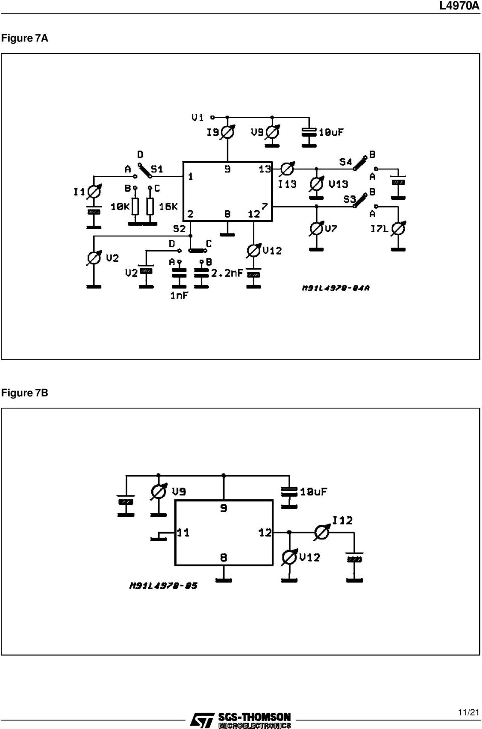
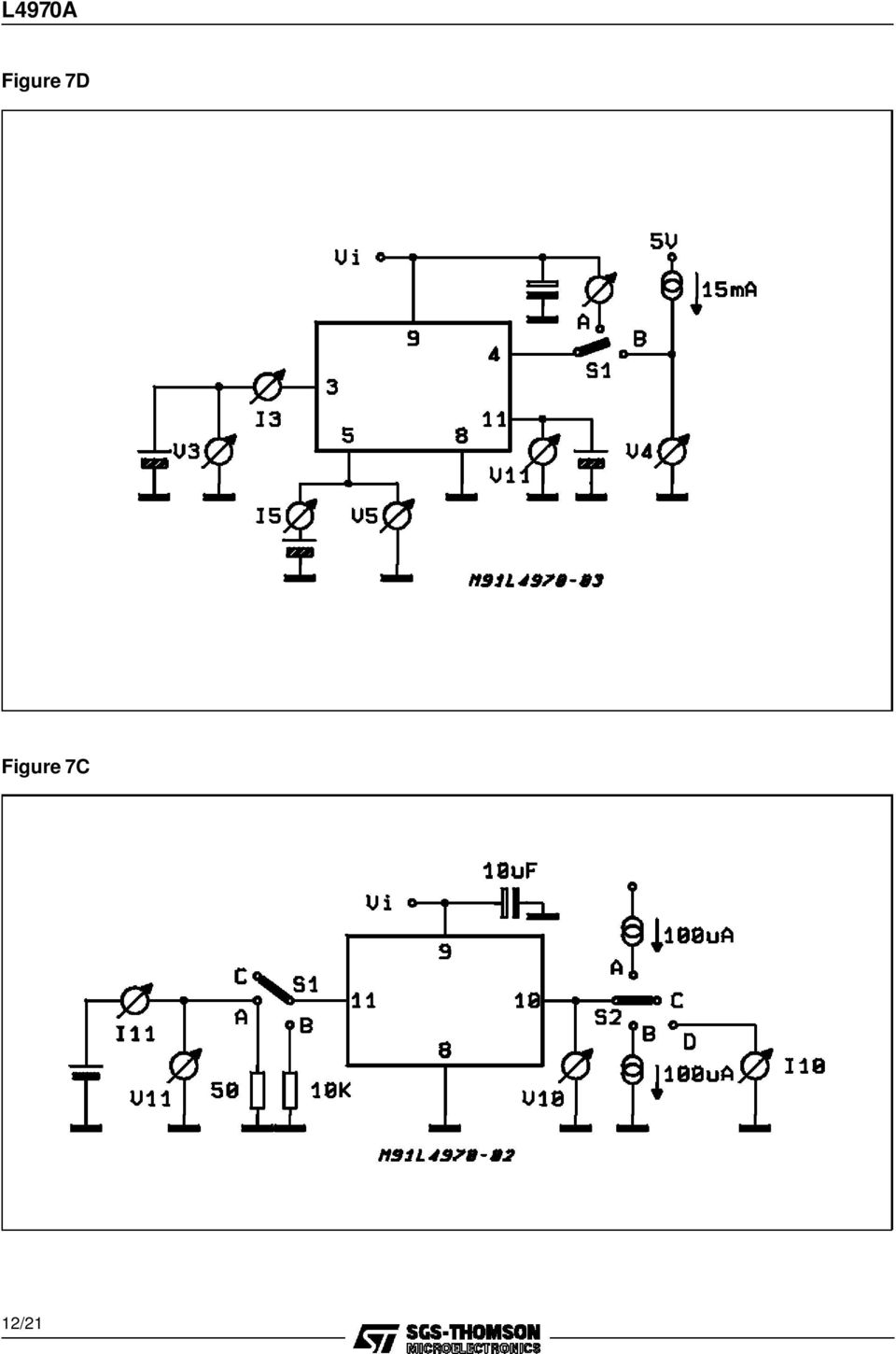
10 Figure 6b: P.C. Board (Back side) and Components Layout of the Circuit of Fig. 5. (1:1 scale) Figure 7: DC Test Circuits 10/21

11 Figure 7A Figure 7B 11/21
12 Figure 7D Figure 7C 12/21
13 Figure 8: Quiescent Drain Current vs. Supply oltage (0% duty cycle - see fig. 7A). Figure 9: Quiescent Drain Current vs. Junction Temperature (0% duty cycle). Figure 10: Quiescent Drain Current vs. Duty Cycle Figure 11: Reference oltage (pin14) vs. i (see fig. 7) Figure 12: Reference oltage (pin 14) vs. Junction Temperature (see fig. 7) Figure 13: Reference oltage (pin15) vs. i (see fig. 7) 13/21
 Figure 12: Reference oltage (pin 14) vs. Junction Temperature (see fig.")
14 Figure 14: Reference oltage (pin 15) vs. Junction Temperature (see fig. 7) Figure 15: Reference oltage 5.1 (pin 14) Supply oltage Ripple Rejection vs. Frequency Figure 16: Switching Frequency vs. Input oltage (see fig. 5) Figure 17: Switching Frequency vs. Junction Temperature (see fig 5) Figure 18: Switching Frequency vs. R4 (see fig. 5) Figure 19: Max. Duty Cycle vs. Frequency 14/21
 Figure 17: Switching Frequency vs.")
15 Figure 20: Supply oltage Ripple Rejection vs. Frequency (see fig. 5) Figure 21: Line Transient Response (see fig. 5) Figure 22: Load Transient Response (see fig. 5) Figure 23: Dropout oltage Between Pin 9 and Pin 7 vs. Current at Pin 7 Figure 24: Dropout oltage Between Pin 9 and Pin 7 vs. Junction Temperature Figure 25: Power Dissipation (device only) vs. Input oltage 15/21
 Figure 23: Dropout oltage Between Pin 9 and Pin 7 vs.")
16 Figure 26: Power Dissipation (device only) vs. Output oltage Figure 27: Heatsink Used to Derive the Device s Power Dissipation Rth - Heatsink = T case T amb P d Figure 28: Efficiency vs. Output Current Figure 29: Efficiency vs. Output oltage Figure 30: Efficiency vs. Output oltage Figure 31: Open Loop Frequency and Phase Response of Error Amplifier (see fig.7c) 16/21

17 Figure 32: Power Dissipation Derating Curve Figure 33: A5.1/12 Multiple Supply. Note the Synchronization between the L4970A and the L4974A 17/21

18 Figure 34: 5.1 / 10A Low Cost Application Figure 35: 10A Switching Regulator, Adjustable from 0 to /21

19 Figure 36: L4970A ssync. Example 19/21

20 MULTIWATT15 PACKAGE MECHANICAL DATA DIM. mm inch MIN. TYP. MAX. MIN. TYP. MAX. A B C D E F G G H H L L L L L L M M S S Dia /21

21 Information furnished is believed to be accurate and reliable. However, SGS-THOMSON Microelectronics assumes no responsibility for the consequences of use of such information nor for any infringement of patents or other rights of third parties which may result from its use. No license is granted by implication or otherwise under any patent or patent rights of SGS-THOMSON Microelectronics. Specifications mentioned in this publication are subject to change without notice. This publication supersedes and replaces all information previously supplied. SGS-THOMSON Microelectronics products are not authorized for use as critical components in life support devices or systems without express written approval of SGS-THOMSON Microelectronics SGS-THOMSON Microelectronics - All RightsReserved MULTIWATT is a Registered Trademark of SGS-THOMSON Microelectronics SGS-THOMSON Microelectronics GROUP OF COMPANIES Australia - Brazil - France - Germany - Hong Kong - Italy - Japan - Korea - Malaysia - Malta - Morocco - The Netherlands - Singapore - Spain - Sweden - Switzerland - Taiwan - Thaliand - United Kingdom - U.S.A. 21/21
SWITCH-MODE POWER SUPPLY CONTROLLER PULSE OUTPUT DC OUTPUT GROUND EXTERNAL FUNCTION SIMULATION ZERO CROSSING INPUT CONTROL EXTERNAL FUNCTION
 SWITCH-MODE POWER SUPPLY CONTROLLER. LOW START-UP CURRENT. DIRECT CONTROL OF SWITCHING TRAN- SISTOR. COLLECTOR CURRENT PROPORTIONAL TO BASE-CURRENT INPUT REERSE-GOING LINEAR OERLOAD CHARACTERISTIC CURE
TDA2040. 20W Hi-Fi AUDIO POWER AMPLIFIER
 20W Hi-Fi AUDIO POWER AMPLIFIER DESCRIPTION The TDA2040 is a monolithic integrated circuit in Pentawatt package, intended for use as an audio class AB amplifier. Typically it provides 22W output power
L293B L293E PUSH-PULL FOUR CHANNEL DRIVERS. OUTPUT CURRENT 1A PER CHANNEL PEAK OUTPUT CURRENT 2A PER CHANNEL (non repetitive) INHIBIT FACILITY
 INHIBIT FACILITY") L293B L293E PUSH-PULL FOUR CHANNEL DRIVERS OUTPUT CURRENT 1A PER CHANNEL PEAK OUTPUT CURRENT 2A PER CHANNEL (non repetitive) INHIBIT FACILITY. HIGH NOISE IMMUNITY SEPARATE LOGIC SUPPLY OVERTEMPERATURE
L293B L293E PUSH-PULL FOUR CHANNEL DRIVERS OUTPUT CURRENT 1A PER CHANNEL PEAK OUTPUT CURRENT 2A PER CHANNEL (non repetitive) INHIBIT FACILITY. HIGH NOISE IMMUNITY SEPARATE LOGIC SUPPLY OVERTEMPERATURE
ADJUSTABLE VOLTAGE AND CURRENT REGULATOR
 L200 ADJUSTABLE VOLTAGE AND CURRENT REGULATOR ADJUSTABLE OUTPUT CURRENT UP TO 2 A (GUARANTEED UP TO Tj = 150 C) ADJUSTABLE OUTPUT VOLTAGE DOWN TO 2.85 V INPUT OVERVOLTAGE PROTECTION (UP TO 60 V, 10 ms)
LF00AB/C SERIES VERY LOW DROP VOLTAGE REGULATORS WITH INHIBIT
 LF00AB/C SERIES ERY LOW DROP OLTAGE REGULATORS WITH INHIBIT ERY LOW DROPOUT OLTAGE (5) ERY LOW QUIESCENT CURRENT (TYP. 50 µa IN OFF MODE, 500µA INON MODE) OUTPUT CURRENT UP TO 500 ma LOGIC-CONTROLLED ELECTRONIC
SG2525A SG3525A REGULATING PULSE WIDTH MODULATORS
 SG2525A SG3525A REGULATING PULSE WIDTH MODULATORS 8 TO 35 V OPERATION 5.1 V REFERENCE TRIMMED TO ± 1 % 100 Hz TO 500 KHz OSCILLATOR RANGE SEPARATE OSCILLATOR SYNC TERMINAL ADJUSTABLE DEADTIME CONTROL INTERNAL
.OPERATING SUPPLY VOLTAGE UP TO 46 V
 L298 DUAL FULL-BRIDGE DRIVER.OPERATING SUPPLY VOLTAGE UP TO 46 V TOTAL DC CURRENT UP TO 4 A. LOW SATURATION VOLTAGE OVERTEMPERATURE PROTECTION LOGICAL "0" INPUT VOLTAGE UP TO 1.5 V (HIGH NOISE IMMUNITY)
TDA4605 CONTROL CIRCUIT FOR SWITCH MODE POWER SUPPLIES USING MOS TRANSISTORS
 CONTROL CIRCUIT FOR SWITCH MODE POWER SUPPLIES USING MOS TRANSISTORS Fold-Back Characteristic provides Overload Protection for External Diodes Burst Operation under Short-Circuit and no Load Conditions
L78M00 SERIES POSITIVE VOLTAGE REGULATORS. www.tvsat.com.pl
 SERIES POSITIVE VOLTAGE REGULATORS OUTPUT CURRENT TO 0.5A OUTPUT VOLTAGES OF 5; 6; 8; 9; 10; 12; 15; 18; 20; 24V THERMAL OVERLOAD PROTECTION SHORT CIRCUIT PROTECTION OUTPUT TRANSISTOR SOA PROTECTION DESCRIPTION
L4940 series VERY LOW DROP 1.5 A REGULATORS
 L4940 series VERY LOW DROP 1.5 A REGULATORS PRECISE 5 V, 8.5 V, 10 V, 12 V OUTPUTS LOW DROPOUT VOLTAGE (500 typ at 1.5A) VERY LOW QUIESCENT CURRENT THERMAL SHUTDOWN SHORT CIRCUIT PROTECTION REVERSE POLARITY
TDA2822 DUAL POWER AMPLIFIER SUPPLY VOLTAGE DOWN TO 3 V LOW CROSSOVER DISTORSION LOW QUIESCENT CURRENT BRIDGE OR STEREO CONFIGURATION
 TDA2822 DUAL POER AMPLIFIER SUPPLY VOLTAGE DON TO 3 V. LO CROSSOVER DISTORSION LO QUIESCENT CURRENT BRIDGE OR STEREO CONFIGURATION DESCRIPTION The TDA2822 is a monolithic integrated circuit in 12+2+2 powerdip,
Symbol Parameter Value Unit V i-o Input-output Differential Voltage 40 V I O Output Current Intenrally Limited Top
 LM117/217 LM317 1.2V TO 37V VOLTAGE REGULATOR OUTPUT VOLTAGE RANGE : 1.2 TO 37V OUTPUT CURRENT IN EXCESS OF 1.5A 0.1% LINE AND LOAD REGULATION FLOATING OPERATION FOR HIGH VOLTAGES COMPLETE SERIES OF PROTECTIONS
TDA2040. 20W Hi-Fi AUDIO POWER AMPLIFIER
 20W Hi-Fi AUDIO POWER AMPLIFIER DESCRIPTION The TDA2040 is a monolithic integrated circuit in Pentawatt package, intended for use as an audio class AB amplifier. Typically it provides 22W output power
CLASS-D VERTICAL DEFLECTION AMPLIFIER FOR TV AND MONITOR APPLICATION OUT CFLY + CFLY - BOOT VREG FEEDCAP FREQ. July 2001 1/8
 CLASS-D VERTICAL DEFLECTION AMPLIFIER FOR TV AND MONITOR APPLICATION FEATURES PRELIMINARY DATA HIGH EFFICIENCY POWER AMPLIFIER NO HEATSINK SPLIT SUPPLY INTERNAL FLYBACK GENERATOR OUTPUT CURRENT UP TO.5
L7800 SERIES POSITIVE VOLTAGE REGULATORS
 SERIES POSITIVE VOLTAGE REGULATORS OUTPUT CURRENT UP TO 1.5 A OUTPUT VOLTAGES OF 5; 5.2; 6; 8; 8.5; 9; 12; 15; 18; 24V THERMAL OVERLOAD PROTECTION SHORT CIRCUIT PROTECTION OUTPUT TRANSITION SOA PROTECTION
HCF4070B QUAD EXCLUSIVE OR GATE
 QUAD EXCLUSIE OR GATE MEDIUM-SPEED OPERATION t PHL = t PLH = 70ns (Typ.) at CL = 50 pf and DD = 10 QUIESCENT CURRENT SPECIFIED UP TO 20 5, 10 AND 15 PARAMETRIC RATINGS INPUT LEAKAGE CURRENT I I = 100nA
HCF4081B QUAD 2 INPUT AND GATE
 QUAD 2 INPUT AND GATE MEDIUM SPEED OPERATION : t PD = 60ns (Typ.) at 10 QUIESCENT CURRENT SPECIFIED UP TO 20 5, 10 AND 15 PARAMETRIC RATINGS INPUT LEAKAGE CURRENT I I = 100nA (MAX) AT DD = 18 T A = 25
HCF4056B BCD TO 7 SEGMENT DECODER /DRIVER WITH STROBED LATCH FUNCTION
 BCD TO 7 SEGMENT DECODER /DRIVER WITH STROBED LATCH FUNCTION QUIESCENT CURRENT SPECIF. UP TO 20V OPERATION OF LIQUID CRYSTALS WITH CMOS CIRCUITS PROVIDES ULTRA LOW POWER DISPLAY. EQUIVALENT AC OUTPUT DRIVE
LM134-LM234 LM334 THREE TERMINAL ADJUSTABLE CURRENT SOURCES. OPERATES from 1V to 40V
 LM134-LM234 LM334 THREE TERMINAL USTABLE CURRENT SOURCES OPERATES from 1 to 40. 0.02% CURRENT REGULATION PROGRAMMABLE from 1µA to 10mA ±3% INITIAL ACCURACY DESCRIPTION The LM134/LM234/LM334 are 3-terminal
L297 STEPPER MOTOR CONTROLLERS
 L297 STEPPER MOTOR CONTROLLERS NORMAL/WAVE DRIVE HALF/FULL STEP MODES CLOCKWISE/ANTICLOCKWISE DIRECTION SWITCHMODE LOAD CURRENT REGULA- TION PROGRAMMABLE LOAD CURRENT FEW EXTERNAL COMPONENTS RESET INPUT
TDA8174A TDA8174AW VERTICAL DEFLECTION CIRCUIT RAMP GENERATOR INDEPENDENT AMPLITUDE ADJUSTEMENT BUFFER STAGE POWER AMPLIFIER
 TDA87A TDA87AW VERTICAL DEFLECTION CIRCUIT RAMP INDEPENDENT AMPLITUDE ADJUSTEMENT BUFFER STAGE POWER AMPLIFIER. FLYBACK THERMAL PROTECTION INTERNAL REFERENCE VOLTAGE DECOU- PLING MULTIWATT (Plastic Package)
BUX48/48A BUV48A/V48AFI
 BUX48/48A BU48A/48AFI HIGH POWER NPN SILICON TRANSISTORS STMicroelectronics PREFERRED SALESTYPES NPN TRANSISTOR HIGH OLTAGE CAPABILITY HIGH CURRENT CAPABILITY FAST SWITCHING SPEED APPLICATIONS SWITCH MODE
. MEDIUM SPEED OPERATION - 8MHz (typ.) @ . MULTI-PACKAGE PARALLEL CLOCKING FOR HCC4029B HCF4029B PRESETTABLE UP/DOWN COUNTER BINARY OR BCD DECADE
 @ . MULTI-PACKAGE PARALLEL CLOCKING FOR HCC4029B HCF4029B PRESETTABLE UP/DOWN COUNTER BINARY OR BCD DECADE") HCC4029B HCF4029B PRESETTABLE UP/DOWN COUNTER BINARY OR BCD DECADE. MEDIUM SPEED OPERATION - 8MHz (typ.) @ CL = 50pF AND DD-SS = 10. MULTI-PACKAGE PARALLEL CLOCKING FOR SYNCHRONOUS HIGH SPEED OUTPUT RES-
HCC4029B HCF4029B PRESETTABLE UP/DOWN COUNTER BINARY OR BCD DECADE. MEDIUM SPEED OPERATION - 8MHz (typ.) @ CL = 50pF AND DD-SS = 10. MULTI-PACKAGE PARALLEL CLOCKING FOR SYNCHRONOUS HIGH SPEED OUTPUT RES-
HCC/HCF4032B HCC/HCF4038B
 HCC/HCF4032B HCC/HCF4038B TRIPLE SERIAL ADDERS INERT INPUTS ON ALL ADDERS FOR SUM COMPLEMENTING APPLICATIONS FULLY STATIC OPERATION...DC TO 10MHz (typ.) @ DD = 10 BUFFERED INPUTS AND OUTPUTS SINGLE-PHASE
MC34063A MC34063E DC-DC CONVERTER CONTROL CIRCUITS
 MC34063A MC34063E DC-DC CONVERTER CONTROL CIRCUITS OUTPUT SWITCH CURRENT IN EXCESS OF 1.5A 2% REFERENCE ACCURACY LOW QUIESCENT CURRENT: 2.5mA (TYP.) OPERATING FROM 3V TO 40V FREQUENCY OPERATION TO 100KHz
HCC4541B HCF4541B PROGRAMMABLE TIMER
 HCC4541B HCF4541B PROGRAMMABLE TIMER 16 STAGE BINARI COUNTER LOW SYMMETRICAL OUTPUT RESISTANCE, TYPICALLY 100 OHM AT DD = 15 OSCILLATOR FREQUENCY RANGE : DC TO 100kHz AUTO OR MASTER RESET DISABLES OSCIL-
STP6N60FI N - CHANNEL ENHANCEMENT MODE POWER MOS TRANSISTOR
 N - CHANNEL ENHANCEMENT MODE POWER MOS TRANSISTOR TYPE VDSS RDS(on) ID STP6N60FI 600 V < 1.2 Ω 3.8 A TYPICAL R DS(on) =1Ω AVALANCHE RUGGED TECHNOLOGY 100% AVALANCHE TESTED REPETITIVE AVALANCHE DATA AT
Obsolete Product(s) - Obsolete Product(s)
 - Obsolete Product(s)") 32 W hi-fi audio power amplifier Features High output power (50 W music power IEC 268.3 rules) High operating supply voltage (50 V) Single or split supply operations Very low distortion Short-circuit protection
32 W hi-fi audio power amplifier Features High output power (50 W music power IEC 268.3 rules) High operating supply voltage (50 V) Single or split supply operations Very low distortion Short-circuit protection
STGW40NC60V N-CHANNEL 50A - 600V - TO-247 Very Fast PowerMESH IGBT
 N-CHANNEL 50A - 600V - TO-247 Very Fast PowerMESH IGBT Table 1: General Features STGW40NC60V 600 V < 2.5 V 50 A HIGH CURRENT CAPABILITY HIGH FREQUENCY OPERATION UP TO 50 KHz LOSSES INCLUDE DIODE RECOVERY
L78MxxAB L78MxxAC. Precision 500 ma regulators. Features. Description
 L78MxxAB L78MxxAC Precision 500 ma regulators Features Output current to 0.5 A Output voltages of 5; 6; 8; 9; 10; 12; 15; 18; 24 V Thermal overload protection Short circuit protection Output transition
STP80NF55-08 STB80NF55-08 STB80NF55-08-1 N-CHANNEL 55V - 0.0065 Ω - 80A D2PAK/I2PAK/TO-220 STripFET II POWER MOSFET
 STP80NF55-08 STB80NF55-08 STB80NF55-08-1 N-CHANNEL 55V - 0.0065 Ω - 80A D2PAK/I2PAK/TO-220 STripFET II POWER MOSFET TYPE V DSS R DS(on) I D STB80NF55-08/-1 STP80NF55-08 55 V 55 V
LM337. Three-terminal adjustable negative voltage regulators. Features. Description
 Three-terminal adjustable negative voltage regulators Datasheet - production data current limit, thermal overload protection and safe area protection. All overload protection circuitry remains fully functional
STP62NS04Z N-CHANNEL CLAMPED 12.5mΩ - 62A TO-220 FULLY PROTECTED MESH OVERLAY MOSFET
 N-CHANNEL CLAMPED 12.5mΩ - 62A TO-220 FULLY PROTECTED MESH OVERLAY MOSFET TYPE V DSS R DS(on) I D STP62NS04Z CLAMPED
TDA2003 10W CAR RADIO AUDIO AMPLIFIER
 TDA2003 10W CAR RADIO AUDIO AMPLIFIER DESCRIPTION The TDA 2003 has improved performance with the same pin configuration as the TDA 2002. The additional features of TDA 2002, very low number of external
Symbol Parameter Value Unit V DS Drain-source Voltage (V GS =0) 50 V V DGR Drain- gate Voltage (R GS =20kΩ) 50 V
 50 V V DGR Drain- gate Voltage (R GS =20kΩ) 50 V") BUZ71A N - CHANNEL 50V - 0.1Ω - 13A TO-220 STripFET POWER MOSFET TYPE V DSS R DS(on) I D BUZ71A 50 V < 0.12 Ω 13 A TYPICAL RDS(on) = 0.1 Ω AVALANCHE RUGGED TECHNOLOGY 100% AVALANCHE TESTED HIGH CURRENT
BUZ71A N - CHANNEL 50V - 0.1Ω - 13A TO-220 STripFET POWER MOSFET TYPE V DSS R DS(on) I D BUZ71A 50 V < 0.12 Ω 13 A TYPICAL RDS(on) = 0.1 Ω AVALANCHE RUGGED TECHNOLOGY 100% AVALANCHE TESTED HIGH CURRENT
LM833 LOW NOISE DUAL OPERATIONAL AMPLIFIER
 LOW NOISE DUAL OPERATIONAL AMPLIFIER LOW VOLTAGE NOISE: 4.5nV/ Hz HIGH GAIN BANDWIDTH PRODUCT: 15MHz HIGH SLEW RATE: 7V/µs LOW DISTORTION:.2% EXCELLENT FREQUENCY STABILITY ESD PROTECTION 2kV DESCRIPTION
TDA2004R. 10 + 10 W stereo amplifier for car radio. Features. Description
 10 + 10 W stereo amplifier for car radio Features Low distortion Low noise Protection against: Output AC short circuit to ground Overrating chip temperature Load dump voltage surge Fortuitous open ground
Symbol Parameter Value Unit IAR Avalanche Current, Repetitive or Not-Repetitive
 BUZ11 N - CHANNEL 50V - 0.03Ω - 30A -TO-220 STripFET POWER MOSFET TYPE V DSS R DS(on) I D BUZ11 50 V < 0.04 Ω 30 A TYPICAL R DS(on) = 0.03 Ω AVALANCHE RUGGED TECHNOLOGY 100% AVALANCHE TESTED HIGH CURRENT
TL074 TL074A - TL074B
 A B LOW NOISE JFET QUAD OPERATIONAL AMPLIFIERS WIDE COMMONMODE (UP TO V + CC ) AND DIFFERENTIAL VOLTAGE RANGE LOW INPUT BIAS AND OFFSET CURRENT LOW NOISE e n = 15nV/ Hz (typ) OUTPUT SHORTCIRCUIT PROTECTION
L6234. Three phase motor driver. Features. Description
 Three phase motor driver Features Supply voltage from 7 to 52 V 5 A peak current R DSon 0.3 Ω typ. value at 25 C Cross conduction protection TTL compatible driver Operating frequency up to 150 khz Thermal
Description. Table 1. Device summary. Order codes. TO-220 (single gauge) TO-220 (double gauge) D²PAK (tape and reel) TO-220FP
 TO-220 (double gauge) D²PAK (tape and reel) TO-220FP") 1.2 V to 37 V adjustable voltage regulators Description Datasheet - production data TO-220 TO-220FP The LM217, LM317 are monolithic integrated circuits in TO-220, TO-220FP and D²PAK packages intended for
1.2 V to 37 V adjustable voltage regulators Description Datasheet - production data TO-220 TO-220FP The LM217, LM317 are monolithic integrated circuits in TO-220, TO-220FP and D²PAK packages intended for
LM1084 5A Low Dropout Positive Regulators
 5A Low Dropout Positive Regulators General Description The LM1084 is a series of low dropout voltage positive regulators with a maximum dropout of 1.5 at 5A of load current. It has the same pin-out as
100V - 100W DMOS AUDIO AMPLIFIER WITH MUTE/ST-BY THERMAL SHUTDOWN STBY-GND
 TDA7294 100V - 100W DMOS AUDIO AMPLIFIER WITH MUTE/ST-BY VERY HIGH OPERATING VOLTAGE RANGE (±40V) DMOS POWER STAGE HIGH OUTPUT POWER (UP TO 100W MU- SIC POWER) MUTING/STAND-BY FUNCTIONS NO SWITCH ON/OFF
VNP5N07 "OMNIFET": FULLY AUTOPROTECTED POWER MOSFET
 "OMNIFET": FULLY AUTOPROTECTED POWER MOSFET TYPE Vclamp RDS(on) Ilim VNP5N07 70 V 0.2 Ω 5 A LINEAR CURRENT LIMITATION THERMAL SHUT DOWN SHORT CIRCUIT PROTECTION INTEGRATED CLAMP LOW CURRENT DRAWN FROM
HCC/HCF4027B DUAL-J-K MASTER-SLAVE FLIP-FLOP
 DUAL-J-K MASTER-SLAVE FLIP-FLOP. SET-RESET CAPABILITY STATIC FLIP-FLOP OPERATION - RETAINS STATE INDEFINITELY WITH CLOCK LEVEL EITHER HIGH OR LOW MEDIUM SPEED OPERATION - 16MHz (typ. clock toggle rate
Description. Table 1. Device summary
 2 A positive voltage regulator IC Description Datasheet - production data Features TO-220 Output current up to 2 A Output voltages of 5; 7.5; 9; 10; 12; 15; 18; 24 V Thermal protection Short circuit protection
Obsolete Product(s) - Obsolete Product(s)
 - Obsolete Product(s)") SYNCHRONOUS PROGRAMMABLE 4-BIT BINARY COUNTER WITH ASYNCHRONOUS CLEAR INTERNAL LOOK-AHEAD FOR FAST COUNTING CARRY OUTPUT FOR CASCADING SYNCHRONOUSLY PROGRAMMABLE LOW-POWER TTL COMPATIBILITY STANDARDIZED
SYNCHRONOUS PROGRAMMABLE 4-BIT BINARY COUNTER WITH ASYNCHRONOUS CLEAR INTERNAL LOOK-AHEAD FOR FAST COUNTING CARRY OUTPUT FOR CASCADING SYNCHRONOUSLY PROGRAMMABLE LOW-POWER TTL COMPATIBILITY STANDARDIZED
TLI4946. Datasheet TLI4946K, TLI4946-2K, TLI4946-2L. Sense and Control. May 2009
 May 2009 TLI4946 High Precision Hall Effect Latches for Industrial and Consumer Applications TLI4946K, TLI4946-2K, TLI4946-2L Datasheet Rev. 1.0 Sense and Control Edition 2009-05-04 Published by Infineon
ULN2801A, ULN2802A, ULN2803A, ULN2804A
 ULN2801A, ULN2802A, ULN2803A, ULN2804A Eight Darlington array Datasheet production data Features Eight Darlington transistors with common emitters Output current to 500 ma Output voltage to 50 V Integral
UNISONIC TECHNOLOGIES CO., LTD
 UPS61 UNISONIC TECHNOLOGIES CO., LTD HIGH PERFORMANCE CURRENT MODE POWER SWITCH DESCRIPTION The UTC UPS61 is designed to provide several special enhancements to satisfy the needs, for example, Power-Saving
STW20NM50 N-CHANNEL 550V @ Tjmax - 0.20Ω - 20ATO-247 MDmesh MOSFET
 N-CHANNEL 550V @ Tjmax - 0.20Ω - 20ATO-247 MDmesh MOSFET TYPE V DSS (@Tjmax) R DS(on) I D STW20NM50 550V < 0.25Ω 20 A TYPICAL R DS (on) = 0.20Ω HIGH dv/dt AND AVALANCHE CAPABILITIES 100% AVALANCHE TESTED
5A 3A. Symbol Parameter Value Unit
 STP5NA50 STP5NA50FI N - CHANNEL ENHANCEMENT MODE FAST POWER MOS TRANSISTOR TYPE VDSS RDS(on) ID STP5NA50 STP5NA50FI 500 V 500 V
.LOW POWER DISSIPATION .HIGH NOISE IMMUNITY M74HC154 4 TO 16 LINE DECODER/DEMULTIPLEXER. HIGH SPEED tpd = 15 ns (TYP.) at VCC =5V
 at VCC =5V") . HIGH SPEED tpd = 15 ns (TYP.) at VCC =5V.LOW POWER DISSIPATION I CC =4µA (MAX.) at T A =25 C.HIGH NOISE IMMUNITY VNIH =VNIL =28%VCC (MIN.) OUTPUT DRIVE CAPABILITY 15 LSTTL LOADS SYMMETRICAL OUTPUT IMPEDANCE
. HIGH SPEED tpd = 15 ns (TYP.) at VCC =5V.LOW POWER DISSIPATION I CC =4µA (MAX.) at T A =25 C.HIGH NOISE IMMUNITY VNIH =VNIL =28%VCC (MIN.) OUTPUT DRIVE CAPABILITY 15 LSTTL LOADS SYMMETRICAL OUTPUT IMPEDANCE
DATA SHEET. TDA8560Q 2 40 W/2 Ω stereo BTL car radio power amplifier with diagnostic facility INTEGRATED CIRCUITS. 1996 Jan 08
 INTEGRATED CIRCUITS DATA SHEET power amplifier with diagnostic facility Supersedes data of March 1994 File under Integrated Circuits, IC01 1996 Jan 08 FEATURES Requires very few external components High
HCF4001B QUAD 2-INPUT NOR GATE
 QUAD 2-INPUT NOR GATE PROPAGATION DELAY TIME: t PD = 50ns (TYP.) at V DD = 10V C L = 50pF BUFFERED INPUTS AND OUTPUTS STANDARDIZED SYMMETRICAL OUTPUT CHARACTERISTICS QUIESCENT CURRENT SPECIFIED UP TO 20V
STP6NK60Z - STP6NK60ZFP STB6NK60Z - STB6NK60Z-1 N-CHANNEL 600V - 1Ω - 6A TO-220/TO-220FP/D 2 PAK/I 2 PAK Zener-Protected SuperMESH Power MOSFET
 STP6NK60Z - STP6NK60ZFP STB6NK60Z - STB6NK60Z-1 N-CHANNEL 600V - 1Ω - 6A TO-220/TO-220FP/D 2 PAK/I 2 PAK Zener-Protected SuperMESH Power MOSFET TYPE V DSS R DS(on) I D Pw STP6NK60Z STP6NK60ZFP STB6NK60Z
Obsolete Product(s) - Obsolete Product(s)
 - Obsolete Product(s)") Vertical deflection booster for 3 App TV/monitor applications with 0 V flyback generator Features Figure. Heptawatt package Power amplifier Flyback generator Stand-by control Output current up to 3.0 App
Vertical deflection booster for 3 App TV/monitor applications with 0 V flyback generator Features Figure. Heptawatt package Power amplifier Flyback generator Stand-by control Output current up to 3.0 App
STP10NK60Z/FP, STB10NK60Z/-1 STW10NK60Z N-CHANNEL 600V-0.65Ω-10A TO-220/FP/D 2 PAK/I 2 PAK/TO-247 Zener-Protected SuperMESH Power MOSFET
 STP10NK60Z/FP, STB10NK60Z/-1 STW10NK60Z N-CHANNEL 600V-0.65Ω-10A TO-220/FP/D 2 PAK/I 2 PAK/TO-247 Zener-Protected SuperMESH Power MOSFET TYPE V DSS R DS(on) I D Pw STP10NK60Z STP10NK60ZFP STB10NK60Z STB10NK60Z-1
IRF830. N - CHANNEL 500V - 1.35Ω - 4.5A - TO-220 PowerMESH MOSFET
 IRF830 N - CHANNEL 500V - 1.35Ω - 4.5A - TO-220 PowerMESH MOSFET TYPE V DSS R DS(on) I D IRF830 500 V < 1.5 Ω 4.5 A TYPICAL R DS(on) = 1.35 Ω EXTREMELY HIGH dv/dt CAPABILITY 100% AVALANCHE TESTED VERY
BTB04-600SL STANDARD 4A TRIAC MAIN FEATURES
 BTB-6SL STANDARD A TRIAC MAIN FEATURES A Symbol Value Unit I T(RMS) A V DRM /V RRM 6 V I GT(Q) ma G A A DESCRIPTION The BTB-6SL quadrants TRIAC is intended for general purpose applications where high surge
IRFP450. N - CHANNEL 500V - 0.33Ω - 14A - TO-247 PowerMESH MOSFET
 IRFP450 N - CHANNEL 500V - 0.33Ω - 14A - TO-247 PowerMESH MOSFET TYPE V DSS R DS(on) I D IRFP450 500 V < 0.4 Ω 14 A TYPICAL R DS(on) = 0.33 Ω EXTREMELY HIGH dv/dt CAPABILITY 100% AVALANCHE TESTED VERY
HCF4028B BCD TO DECIMAL DECODER
 BCD TO DECIMAL DECODER BCD TO DECIMAL DECODING OR BINARY TO OCTAL DECODING HIGH DECODED OUTPUT DRIVE CAPABILITY "POSITIVE LOGIC" INPUTS AND OUTPUTS: DECODED OUTPUTS GO HIGH ON SELECTION MEDIUM SPEED OPERATION
Programmable Single-/Dual-/Triple- Tone Gong SAE 800
 Programmable Single-/Dual-/Triple- Tone Gong Preliminary Data SAE 800 Bipolar IC Features Supply voltage range 2.8 V to 18 V Few external components (no electrolytic capacitor) 1 tone, 2 tones, 3 tones
CA723, CA723C. Voltage Regulators Adjustable from 2V to 37V at Output Currents Up to 150mA without External Pass Transistors. Features.
 CA73, CA73C Data Sheet April 1999 File Number 788. Voltage Regulators Adjustable from V to 37V at Output Currents Up to 1mA without External Pass Transistors The CA73 and CA73C are silicon monolithic integrated
VN03. ISO high side smart power solid state relay PENTAWATT. Features. Description. www.tvsat.com.pl
 ISO high side smart power solid state relay Features Type V DSS R DS(on) I n (1) Maximum continuous output current (a) : 4A @ Tc= 25 C 5V logic level compatible input Thermal shutdown Under voltage protection
LM78XX Series Voltage Regulators
 LM78XX Series Voltage Regulators General Description Connection Diagrams The LM78XX series of three terminal regulators is available with several fixed output voltages making them useful in a wide range
IRF740 N-CHANNEL 400V - 0.46Ω - 10A TO-220 PowerMESH II MOSFET
 N-CHANNEL 400V - 0.46Ω - 10A TO-220 PowerMESH II MOSFET TYPE V DSS R DS(on) I D IRF740 400 V < 0.55 Ω 10 A TYPICAL R DS (on) = 0.46Ω EXCEPTIONAL dv/dt CAPABILITY 100% AVALANCHE TESTED LOW GATE CHARGE VERY
STW34NB20 N-CHANNEL 200V - 0.062 Ω - 34A TO-247 PowerMESH MOSFET
 N-CHANNEL 200V - 0.062 Ω - 34A TO-247 PowerMESH MOSFET Table 1. General Features Figure 1. Package Type V DSS R DS(on) I D STW34NB20 200 V < 0.075 Ω 34 A FEATURES SUMMARY TYPICAL R DS(on) = 0.062 Ω EXTREMELY
STCS1. 1.5 A max constant current LED driver. Features. Applications. Description
 1.5 A max constant current LED driver Features Up to 40 V input voltage Less than 0.5 V voltage overhead Up to 1.5 A output current PWM dimming pin Shutdown pin LED disconnection diagnostic DFN8 (3x3 mm)
STCS1A. 1.5 A max constant current LED driver. Features. Applications. Description
 1.5 A max constant current LED driver Features Up to 40 V input voltage Less than 0.5 V voltage overhead Up to 1.5 A output current PWM dimming pin Shutdown pin LED disconnection diagnostic DFN8 (3 x 3
AAT4280 Slew Rate Controlled Load Switch
 General Description Features SmartSwitch The AAT4280 SmartSwitch is a P-channel MOSFET power switch designed for high-side load switching applications. The P-channel MOSFET device has a typical R DS(ON)
AS2815. 1.5A Low Dropout Voltage Regulator Adjustable & Fixed Output, Fast Response
 1.5A Low Dropout oltage Regulator Adjustable & Fixed Output, Fast Response FEATURES Adjustable Output Down To 1.2 Fixed Output oltages 1.5, 2.5, 3.3, 5.0 Output Current of 1.5A Low Dropout oltage 1.1 Typ.
BD238. Low voltage PNP power transistor. Features. Applications. Description. Low saturation voltage PNP transistor
 Low voltage PNP power transistor Features Low saturation voltage PNP transistor Applications Audio, power linear and switching applications Description The device is manufactured in planar technology with
unit : mm With heat sink (see Pd Ta characteristics)
") Ordering number: EN1321E Monolithic Linear IC LA4261 3.5 W 2-Channel AF Power Amplifier for Home Stereos and Music Centers Features. Minimum number of external parts required (No input capacitor, bootstrap
Ordering number: EN1321E Monolithic Linear IC LA4261 3.5 W 2-Channel AF Power Amplifier for Home Stereos and Music Centers Features. Minimum number of external parts required (No input capacitor, bootstrap
TL084 TL084A - TL084B
 A B GENERAL PURPOSE JFET QUAD OPERATIONAL AMPLIFIERS WIDE COMMONMODE (UP TO V + CC ) AND DIFFERENTIAL VOLTAGE RANGE LOW INPUT BIAS AND OFFSET CURRENT OUTPUT SHORTCIRCUIT PROTECTION HIGH INPUT IMPEDANCE
STCS2A. 2 A max constant current LED driver. Features. Applications. Description
 2 A max constant current LED driver Features Up to 40 V input voltage Less than 0.5 V voltage overhead Up to 2 A output current PWM dimming pin Shutdown pin LED disconnection diagnostic Slope control with
TDA7448 6 CHANNEL VOLUME CONTROLLER 1 FEATURES 2 DESCRIPTION. Figure 1. Package
 6 CHANNEL CONTROLLER FEATURES 6 CHANNEL INPUTS 6 CHANNEL OUTPUTS ATTENUATION RANGE OF 0 TO -79dB CONTROL IN.0dB STEPS 6 CHANNEL INDEPENDENT CONTROL ALL FUNCTION ARE PROGRAMMABLE VIA SERIAL BUS DESCRIPTION
L6201 L6202 - L6203 DMOS FULL BRIDGE DRIVER
 L6201 L6202 - L6203 DMOS FULL BRIDGE DRIVER SUPPLY VOLTAGE UP TO 48V 5A MAX PEAK CURRENT (2A max. for L6201) TOTAL RMS CURRENT UP TO L6201: 1A; L6202: 1.5A; L6203/L6201PS: 4A RDS (ON) 0.3 Ω (typical value
DATA SHEET. TDA1510AQ 24 W BTL or 2 x 12 W stereo car radio power amplifier INTEGRATED CIRCUITS
 INTEGRATED CIRCUITS DATA SHEET 24 W BTL or 2 x 12 W stereo car radio File under Integrated Circuits, IC01 January 1992 GENERAL DESCRIPTION The is a class-b integrated output amplifier encapsulated in a
ST1S10. 3 A, 900 khz, monolithic synchronous step-down regulator. Features. Description. Applications
 3 A, 900 khz, monolithic synchronous step-down regulator Features Step-down current mode PWM regulator Output voltage adjustable from 0.8 V Input voltage from 2.5 V up to 18 V 2% DC output voltage tolerance
STB4NK60Z, STB4NK60Z-1, STD4NK60Z STD4NK60Z-1, STP4NK60Z,STP4NK60ZFP
 STB4NK60Z, STB4NK60Z-1, STD4NK60Z STD4NK60Z-1, STP4NK60Z,STP4NK60ZFP N-channel 600 V - 1.76 Ω - 4 A SuperMESH Power MOSFET DPAK - D 2 PAK - IPAK - I 2 PAK - TO-220 - TO-220FP Features Type V DSS R DS(on)
Description SO-8. series. Furthermore, in the 8-pin configuration Very low-dropout voltage (0.2 V typ.)
") ery low-dropout voltage regulator with inhibit function TO-92 Bag TO-92 Tape and reel Ammopack 1 2 3 SO-8 Description Datasheet - production data The is a very low-dropout voltage regulator available in
ery low-dropout voltage regulator with inhibit function TO-92 Bag TO-92 Tape and reel Ammopack 1 2 3 SO-8 Description Datasheet - production data The is a very low-dropout voltage regulator available in
LM134-LM234-LM334. Three terminal adjustable current sources. Features. Description
 Three terminal adjustable current sources Features Operates from 1V to 40V 0.02%/V current regulation Programmable from 1µA to 10mA ±3% initial accuracy Description The LM134/LM234/LM334 are 3-terminal
LM2576R. 3.0A, 52kHz, Step-Down Switching Regulator FEATURES. Applications DESCRIPTION TO-220 PKG TO-220V PKG TO-263 PKG ORDERING INFORMATION
 LM2576 FEATURES 3.3, 5.0, 12, 15, and Adjustable Output ersions Adjustable ersion Output oltage Range, 1.23 to 37 +/- 4% AG10Maximum Over Line and Load Conditions Guaranteed 3.0A Output Current Wide Input
Transistor MOS. Ce Dossier comporte 10 pages comme suit : - Page 1 : Fonctionnement du transistor MOS
 Transistor MOS Ce Dossier comporte 10 pages comme suit : - Page 1 : Fonctionnement du transistor MOS - Pages 2 à 9 : Documentation constructeur VNP49N04 NOTA : Tous les documents fournis seront remis à
UC3842/UC3843/UC3844/UC3845
 SMPS Controller www.fairchildsemi.com Features Low Start up Current Maximum Duty Clamp UVLO With Hysteresis Operating Frequency up to 500KHz Description The UC3842/UC3843/UC3844/UC3845 are fixed frequencycurrent-mode
VN05N. High side smart power solid state relay PENTAWATT. Features. Description
 High side smart power solid state relay Features Type V DSS R DS(on) I OUT V CC VN05N 60 V 0.18 Ω 13 A 26 V Output current (continuous): 13A @ Tc=25 C 5V logic level compatible input Thermal shutdown Under
MC34063AB, MC34063AC, MC34063EB, MC34063EC
 MC34063AB, MC34063AC, MC34063EB, MC34063EC DC-DC converter control circuits Description Datasheet - production data Features DIP-8 SO-8 Output switch current in excess of 1.5 A 2 % reference accuracy Low
HCF4010B HEX BUFFER/CONVERTER (NON INVERTING)
") HEX BUFFER/CONVERTER (NON INVERTING) PROPAGATION DELAY TIME: t PD = 50ns (Typ.) at V DD = 10V C L = 50pF HIGH TO LOW LEVEL LOGIC CONVERSION MULTIPLEXER: 1 TO 6 OR 6 TO 1 HIGH "SINK" AND "SOURCE" CURRENT
HEX BUFFER/CONVERTER (NON INVERTING) PROPAGATION DELAY TIME: t PD = 50ns (Typ.) at V DD = 10V C L = 50pF HIGH TO LOW LEVEL LOGIC CONVERSION MULTIPLEXER: 1 TO 6 OR 6 TO 1 HIGH "SINK" AND "SOURCE" CURRENT
KA7500C. SMPS Controller. Features. Description. Internal Block Diagram. www.fairchildsemi.com
 SMPS Controller www.fairchildsemi.com Features Internal Regulator Provides a Stable 5V Reference Supply Trimmed to ±1% Accuracy. Uncommitted Output TR for 200mA Sink or Source Current Output Control for
Baseband delay line QUICK REFERENCE DATA
 FEATURES Two comb filters, using the switched-capacitor technique, for one line delay time (64 µs) Adjustment-free application No crosstalk between SECAM colour carriers (diaphoty) Handles negative or
. HIGH SPEED .LOW POWER DISSIPATION .COMPATIBLE WITH TTL OUTPUTS M54HCT27 M74HCT27 TRIPLE 3-INPUT NOR GATE. tpd = 9 ns (TYP.
 M54HCT27 M74HCT27 TRIPLE 3-INPUT NOR GATE. HIGH SPEED tpd = 9 ns (TYP.) AT VCC =5V.LOW POWER DISSIPATION I CC =1µA (MAX.) AT T A =25 C.COMPATIBLE WITH TTL OUTPUTS VIH = 2V (MIN.) VIL = 0.8V (MAX) OUTPUT
TDA7318D DIGITAL CONTROLLED STEREO AUDIO PROCESSOR
 TDA738 DIGITAL CONTROLLED STEREO AUDIO PROCESSOR INPUT MULTIPLEXER: - 4 STEREO INPUTS - SELECTABLE INPUT GAIN FOR OPTIMAL ADAPTION TO DIFFERENT SOURCES INPUT AND OUTPUT FOR EXTERNAL EQUALIZER OR NOISE
TL783C, TL783Y HIGH-VOLTAGE ADJUSTABLE REGULATOR
 HIGH-VOLTAGE USTABLE REGULATOR SLVS36C SEPTEMBER 1981 REVISED APRIL 1997 Output Adjustable From 1.25 V to 125 V When Used With an External Resistor Divider 7-mA Output Current Full Short-Circuit, Safe-Operating-Area,
BD241A BD241C. NPN power transistors. Features. Applications. Description. NPN transistors. Audio, general purpose switching and amplifier transistors
 BD241A BD241C NPN power transistors Features. NPN transistors Applications Audio, general purpose switching and amplifier transistors Description The devices are manufactured in Planar technology with
SELF-OSCILLATING HALF-BRIDGE DRIVER
 Data Sheet No. PD60029 revj I2155&(PbF) (NOTE: For new designs, we recommend I s new products I2153 and I21531) SELF-OSCILLATING HALF-BIDGE DIE Features Floating channel designed for bootstrap operation
PAM2804. Pin Assignments. Description. Applications. Features. Typical Applications Circuit 1A STEP-DOWN CONSTANT CURRENT, HIGH EFFICIENCY LED DRIVER
 1A STEP-DOWN CONSTANT CURRENT, HIGH EFFICIENCY LED DRIER Description Pin Assignments The is a step-down constant current LED driver. When the input voltage is down to lower than LED forward voltage, then
MP2259 1A, 16V, 1.4MHz Step-Down Converter
 MP59 1A, 1V, 1.MHz Step-Down Converter TM The Future of Analog IC Technology DESCRIPTION The MP59 is a monolithic integrated stepdown switch mode converter with an internal power MOSFET. It achieves 1A
NTE923 & NTE923D Integrated Circuit Precision Voltage Regulator
 NTE923 & NTE923D Integrated Circuit Precision Voltage Regulator Description: The NTE923 and NTE923D are voltage regulators designed primarily for series regulator applications. By themselves, these devices
www.jameco.com 1-800-831-4242
 Distributed by: www.jameco.com 1-800-831-4242 The content and copyrights of the attached material are the property of its owner. LF411 Low Offset, Low Drift JFET Input Operational Amplifier General Description