CMOS Digital Circuits
|
|
|
- Mavis Crawford
- 7 years ago
- Views:
Transcription
1 CMOS Digital Circuits Types of Digital Circuits Combinational The value of the outputs at any time t depends only on the combination of the values applied at the inputs at time t (the system has no memory) Sequential The value of the outputs at any time t depends not only on the values applied at the inputs at time t, but also on the past sequence of inputs that have been applied (the system has memory) 1

2 Logic values and noise margins VOH VOL noise VIH VIL VOH VIH VOL VIL 2

3 MOS Transistors Four terminals: gate, source, drain, body (= bulk) 3

4 Silicon Lattice Transistors are built on a silicon substrate Silicon is a semiconductor (Group IV material) Forms crystal lattice with bonds to four neighbors 4

5 Dopant atoms Pure silicon has no free carriers and conducts poorly. Adding dopants increases the conductivity Group V: extra electron (n-type) Group III: missing electron, called hole (p-type) Si Si - Si Si Si + Si Si + As Si Si B - Si Si Si Si Si Si Si 5
 Group III: missing electron, called hole")
6 Types of Transistor Bipolar Junction Transistor (BJT) NPN and PNP transistors Small current into very thin base layer controls large current between emitter and collector Base currents limit integration density MOS Field Effect Transistor (MOSFET) NMOS and PMOS FETs Voltage applied to insulated gate controls current between source and drain Low power allows very high integration 6

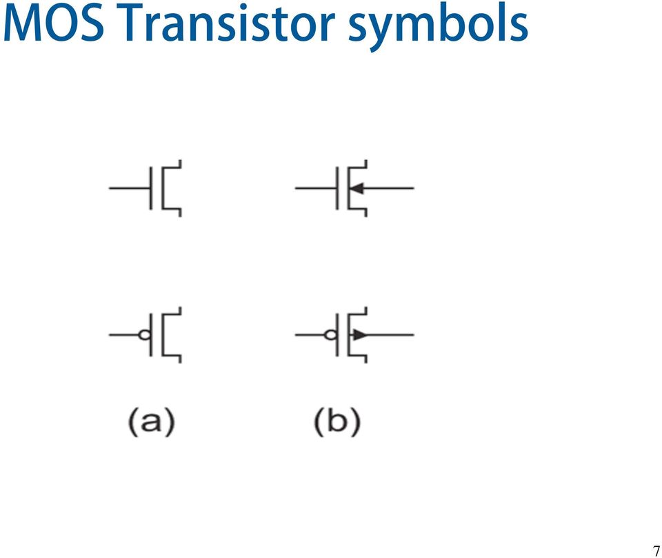
7 MOS Transistor symbols 7
8 N-MOSFET operation (1) Body is commonly tied to ground (0 V) When the gate is at a low voltage: P-type body is at low voltage Source-body and drain-body diodes are OFF No current flows, transistor is OFF Source Gate Drain Polysilicon SiO 2 n+ p n+ bulk Si S 0 D 8

9 N-MOSFET operation (2) When the gate is at a high voltage: Positive charge on gate of MOS capacitor Negative charge attracted to body channel under gate gets inverted to n-type Now current can flow through n-type silicon from source through channel to drain, transistor is ON Source Gate Drain Polysilicon SiO 2 n+ p n+ bulk Si S 1 D 9

10 P-MOSFET operation Similar BUT doping and voltages are reversed Body tied to high voltage (V DD ) Gate low : transistor ON Gate high : transistor OFF Bubble indicates inverted behavior Polysilicon Source Gate Drain SiO 2 p+ p+ n bulk Si 10

11 What does high and low voltage really means? Power Supply Voltage: GND = 0 V In 1980 s, V DD = 5V V DD has decreased in modern processes High V DD would damage modern tiny transistors Lower V DD saves power V DD = 3.3, 2.5, 1.8, 1.5, 1.2, 1.0, 11

12 MOSFETs as SWITCHES We can model MOS transistors as controlled switches Voltage at gate controls current path from source to drain 12

13 CMOS Inverter (= NOT gate) 13
 13")
14 CMOS Technology CMOS technology uses both nmos and pmos transistors The transistors are arranged in a structure formed by two complementary networks Pull-up network is complement of pull-down network Parallel Series Series Parallel 14

15 CMOS Logic NAND 15

16 CMOS Logic NOR 16

17 CMOS logic gates (a.k.a. Static CMOS) Pull-up network is complement of pull-down Parallel Series Series Parallel 17

18 Compound gates Example: ( A+B+C ) D VDD A B C D Y A D Y B C 18

19 Compound gates 19

20 How good is the output signal? Strength of signal How close the signal approximate ideal voltage source VDD and GND rails are the strongest 1 and 0 nmos and pmos are not ideal switches THUS: pmos passes strong 1, but degraded (weak) 0 nmos passes strong 0. but degraded (weak) 1 nmos are best for the pull-down network pmos are best for the pull-up network 20
 0 nmos passes strong 0.")
21 The Pass Transistor Transistors used as switches 21
22 The Transmission Gate Pass transistors produce degraded outputs Transmission gates pass both 0 and 1 well 22
23 Static CMOS gates are fully restoring In static CMOS, the nmos transistors only need to pass 0 s and the pmos only pass 1 s, so the output is always strongly driven and the levels are never degraded This is called a fully restoring logic gate 23
24 Static CMOS is inherently inverting CMOS single stage gates must be inverting For building non inverting functions we need multiple stages 24
25 Tristate Buffer A tristate buffer produce Z when not enabled A EN Y 0 0 Z Z
26 Non restoring tristate Transmission gate acts as tristate buffer It takes only 2 transistors BUT is nonrestoring A is passed to Y as it is (thus, Y is not always a strong 0 or 1) 26
27 Tristate inverter Tristate inverter produces restored output For a non inverting tristate add an inverter in front 27
28 Designing a 2:1 mux D0 D1 S Y
29 2:1 mux - gate level approach Y =D0 S+D1 S D1 S D0 Y D1 S D Y How many transistors are needed? Too Many!!! (20 transistors) 29
30 2:1 mux TG approach We need only 4 transistors (6 to be honest) BUT it is non restoring and it has another issue called charge sharing LOW S = 1 0 HIGH Cap (charged) 30
31 inverting mux VDD D0 D1 31
32 D Latch When CLK = 1, latch is transparent D flows through to Q like a buffer When CLK = 0, the latch is opaque Q holds its old value independent of D a.k.a. transparent latch or level-sensitive latch 32
33 D Latch Design and Operation Multiplexer chooses D or hold Q 33
34 D Flip Flop When CLK rises, D is copied to Q At all other times, Q holds its value a.k.a. positive edge-triggered flip-flop, master-slave flip-flop 34
35 D Flip Flop Design and Operation Built from master and slave D Laches 35
Introduction to CMOS VLSI Design
 Introduction to CMOS VLSI esign Slides adapted from: N. Weste,. Harris, CMOS VLSI esign, Addison-Wesley, 3/e, 24 Introduction Integrated Circuits: many transistors on one chip Very Large Scale Integration
Chapter 10 Advanced CMOS Circuits
 Transmission Gates Chapter 10 Advanced CMOS Circuits NMOS Transmission Gate The active pull-up inverter circuit leads one to thinking about alternate uses of NMOS devices. Consider the circuit shown in
Module 7 : I/O PADs Lecture 33 : I/O PADs
 Module 7 : I/O PADs Lecture 33 : I/O PADs Objectives In this lecture you will learn the following Introduction Electrostatic Discharge Output Buffer Tri-state Output Circuit Latch-Up Prevention of Latch-Up
Here we introduced (1) basic circuit for logic and (2)recent nano-devices, and presented (3) some practical issues on nano-devices.
 basic circuit for logic and (2)recent nano-devices, and presented (3) some practical issues on nano-devices.") Outline Here we introduced () basic circuit for logic and (2)recent nano-devices, and presented (3) some practical issues on nano-devices. Circuit Logic Gate A logic gate is an elemantary building block
Outline Here we introduced () basic circuit for logic and (2)recent nano-devices, and presented (3) some practical issues on nano-devices. Circuit Logic Gate A logic gate is an elemantary building block
The MOSFET Transistor
 The MOSFET Transistor The basic active component on all silicon chips is the MOSFET Metal Oxide Semiconductor Field Effect Transistor Schematic symbol G Gate S Source D Drain The voltage on the gate controls
Lecture 10 Sequential Circuit Design Zhuo Feng. Z. Feng MTU EE4800 CMOS Digital IC Design & Analysis 2010
 EE4800 CMOS igital IC esign & Analysis Lecture 10 Sequential Circuit esign Zhuo Feng 10.1 Z. Feng MTU EE4800 CMOS igital IC esign & Analysis 2010 Sequencing Outline Sequencing Element esign Max and Min-elay
ECE124 Digital Circuits and Systems Page 1
 ECE124 Digital Circuits and Systems Page 1 Chip level timing Have discussed some issues related to timing analysis. Talked briefly about longest combinational path for a combinational circuit. Talked briefly
Field-Effect (FET) transistors
 transistors") Field-Effect (FET) transistors References: Hayes & Horowitz (pp 142-162 and 244-266), Rizzoni (chapters 8 & 9) In a field-effect transistor (FET), the width of a conducting channel in a semiconductor and,
Field-Effect (FET) transistors References: Hayes & Horowitz (pp 142-162 and 244-266), Rizzoni (chapters 8 & 9) In a field-effect transistor (FET), the width of a conducting channel in a semiconductor and,
1. True or False? A voltage level in the range 0 to 2 volts is interpreted as a binary 1.
 File: chap04, Chapter 04 1. True or False? A voltage level in the range 0 to 2 volts is interpreted as a binary 1. 2. True or False? A gate is a device that accepts a single input signal and produces one
Lecture 11: Sequential Circuit Design
 Lecture 11: Sequential Circuit esign Outline Sequencing Sequencing Element esign Max and Min-elay Clock Skew Time Borrowing Two-Phase Clocking 2 Sequencing Combinational logic output depends on current
Semiconductors, diodes, transistors
 Semiconductors, diodes, transistors (Horst Wahl, QuarkNet presentation, June 2001) Electrical conductivity! Energy bands in solids! Band structure and conductivity Semiconductors! Intrinsic semiconductors!
Layout of Multiple Cells
 Layout of Multiple Cells Beyond the primitive tier primitives add instances of primitives add additional transistors if necessary add substrate/well contacts (plugs) add additional polygons where needed
Sequential 4-bit Adder Design Report
 UNIVERSITY OF WATERLOO Faculty of Engineering E&CE 438: Digital Integrated Circuits Sequential 4-bit Adder Design Report Prepared by: Ian Hung (ixxxxxx), 99XXXXXX Annette Lo (axxxxxx), 99XXXXXX Pamela
Theory of Transistors and Other Semiconductor Devices
 Theory of Transistors and Other Semiconductor Devices 1. SEMICONDUCTORS 1.1. Metals and insulators 1.1.1. Conduction in metals Metals are filled with electrons. Many of these, typically one or two per
Lecture 10: Sequential Circuits
 Introduction to CMOS VLSI esign Lecture 10: Sequential Circuits avid Harris Harvey Mudd College Spring 2004 Outline q Sequencing q Sequencing Element esign q Max and Min-elay q Clock Skew q Time Borrowing
EDC Lesson 12: Transistor and FET Characteristics. 2008 EDCLesson12- ", Raj Kamal, 1
 EDC Lesson 12: Transistor and FET Characteristics Lesson-12: MOSFET (enhancement and depletion mode) Characteristics and Symbols 2008 EDCLesson12- ", Raj Kamal, 1 1. Metal Oxide Semiconductor Field Effect
Sequential Circuits. Combinational Circuits Outputs depend on the current inputs
 Principles of VLSI esign Sequential Circuits Sequential Circuits Combinational Circuits Outputs depend on the current inputs Sequential Circuits Outputs depend on current and previous inputs Requires separating
W04 Transistors and Applications. Yrd. Doç. Dr. Aytaç Gören
 W04 Transistors and Applications W04 Transistors and Applications ELK 2018 - Contents W01 Basic Concepts in Electronics W02 AC to DC Conversion W03 Analysis of DC Circuits (self and condenser) W04 Transistors
Bipolar Junction Transistor Basics
 by Kenneth A. Kuhn Sept. 29, 2001, rev 1 Introduction A bipolar junction transistor (BJT) is a three layer semiconductor device with either NPN or PNP construction. Both constructions have the identical
Advanced VLSI Design CMOS Processing Technology
 Isolation of transistors, i.e., their source and drains, from other transistors is needed to reduce electrical interactions between them. For technologies
Content Map For Career & Technology
 Content Strand: Applied Academics CT-ET1-1 analysis of electronic A. Fractions and decimals B. Powers of 10 and engineering notation C. Formula based problem solutions D. Powers and roots E. Linear equations
Introduction to VLSI Fabrication Technologies. Emanuele Baravelli
 Introduction to VLSI Fabrication Technologies Emanuele Baravelli 27/09/2005 Organization Materials Used in VLSI Fabrication VLSI Fabrication Technologies Overview of Fabrication Methods Device simulation
CHAPTER 10 Fundamentals of the Metal Oxide Semiconductor Field Effect Transistor
 CHAPTER 10 Fundamentals of the Metal Oxide Semiconductor Field Effect Transistor Study the characteristics of energy bands as a function of applied voltage in the metal oxide semiconductor structure known
Statistical Models for Hot Electron Degradation in Nano-Scaled MOSFET Devices
 2006, 대한 산업공학회 추계학술대회 Session C3 : Statistical models Statistical Models for Hot Electron Degradation in Nano-Scaled MOSFET Devices Seong-joon Kim, Suk Joo Bae Dept. of Industrial Engineering, Hanyang
Bob York. Transistor Basics - MOSFETs
 Bob York Transistor Basics - MOSFETs Transistors, Conceptually So far we have considered two-terminal devices that are described by a current-voltage relationship I=f(V Resistors: Capacitors: Inductors:
Solid-State Physics: The Theory of Semiconductors (Ch. 10.6-10.8) SteveSekula, 30 March 2010 (created 29 March 2010)
 SteveSekula, 30 March 2010 (created 29 March 2010)") Modern Physics (PHY 3305) Lecture Notes Modern Physics (PHY 3305) Lecture Notes Solid-State Physics: The Theory of Semiconductors (Ch. 10.6-10.8) SteveSekula, 30 March 2010 (created 29 March 2010) Review
Modern Physics (PHY 3305) Lecture Notes Modern Physics (PHY 3305) Lecture Notes Solid-State Physics: The Theory of Semiconductors (Ch. 10.6-10.8) SteveSekula, 30 March 2010 (created 29 March 2010) Review
Interfacing 3V and 5V applications
 Authors: Tinus van de Wouw (Nijmegen) / Todd Andersen (Albuquerque) 1.0 THE NEED FOR TERFACG BETWEEN 3V AND 5V SYSTEMS Many reasons exist to introduce 3V 1 systems, notably the lower power consumption
Application Note AN-940
 Application Note AN-940 How P-Channel MOSFETs Can Simplify Your Circuit Table of Contents Page 1. Basic Characteristics of P-Channel HEXFET Power MOSFETs...1 2. Grounded Loads...1 3. Totem Pole Switching
MOS Transistors as Switches
 MOS Transistors as Switches G (gate) nmos transistor: Closed (conducting) when Gate = 1 (V DD ) D (drain) S (source) Oen (non-conducting) when Gate = 0 (ground, 0V) G MOS transistor: Closed (conducting)
ECE380 Digital Logic
 ECE38 igital Logic Flip-Flops, Registers and Counters: Flip-Flops r.. J. Jackson Lecture 25- Flip-flops The gated latch circuits presented are level sensitive and can change states more than once during
Memory Elements. Combinational logic cannot remember
 Memory Elements Combinational logic cannot remember Output logic values are function of inputs only Feedback is needed to be able to remember a logic value Memory elements are needed in most digital logic
Class 11: Transmission Gates, Latches
 Topics: 1. Intro 2. Transmission Gate Logic Design 3. X-Gate 2-to-1 MUX 4. X-Gate XOR 5. X-Gate 8-to-1 MUX 6. X-Gate Logic Latch 7. Voltage Drop of n-ch X-Gates 8. n-ch Pass Transistors vs. CMOS X-Gates
NEW adder cells are useful for designing larger circuits despite increase in transistor count by four per cell.
 CHAPTER 4 THE ADDER The adder is one of the most critical components of a processor, as it is used in the Arithmetic Logic Unit (ALU), in the floating-point unit and for address generation in case of cache
Clocking. Figure by MIT OCW. 6.884 - Spring 2005 2/18/05 L06 Clocks 1
 ing Figure by MIT OCW. 6.884 - Spring 2005 2/18/05 L06 s 1 Why s and Storage Elements? Inputs Combinational Logic Outputs Want to reuse combinational logic from cycle to cycle 6.884 - Spring 2005 2/18/05
Lecture 060 Push-Pull Output Stages (1/11/04) Page 060-1. ECE 6412 - Analog Integrated Circuits and Systems II P.E. Allen - 2002
 Page 060-1. ECE 6412 - Analog Integrated Circuits and Systems II P.E. Allen - 2002") Lecture 060 PushPull Output Stages (1/11/04) Page 0601 LECTURE 060 PUSHPULL OUTPUT STAGES (READING: GHLM 362384, AH 226229) Objective The objective of this presentation is: Show how to design stages that
Lecture 060 PushPull Output Stages (1/11/04) Page 0601 LECTURE 060 PUSHPULL OUTPUT STAGES (READING: GHLM 362384, AH 226229) Objective The objective of this presentation is: Show how to design stages that
CMOS Logic Integrated Circuits
 CMOS Logic Integrated Circuits Introduction CMOS Inverter Parameters of CMOS circuits Circuits for protection Output stage for CMOS circuits Buffering circuits Introduction Symetrical and complementary
Fabrication and Manufacturing (Basics) Batch processes
 Batch processes") Fabrication and Manufacturing (Basics) Batch processes Fabrication time independent of design complexity Standard process Customization by masks Each mask defines geometry on one layer Lower-level masks
Fabrication and Manufacturing (Basics) Batch processes Fabrication time independent of design complexity Standard process Customization by masks Each mask defines geometry on one layer Lower-level masks
ANALOG & DIGITAL ELECTRONICS
 ANALOG & DIGITAL ELECTRONICS Course Instructor: Course No: PH-218 3-1-0-8 Dr. A.P. Vajpeyi E-mail: apvajpeyi@iitg.ernet.in Room No: #305 Department of Physics, Indian Institute of Technology Guwahati,
Sequential Logic Design Principles.Latches and Flip-Flops
 Sequential Logic Design Principles.Latches and Flip-Flops Doru Todinca Department of Computers Politehnica University of Timisoara Outline Introduction Bistable Elements Latches and Flip-Flops S-R Latch
Gates, Circuits, and Boolean Algebra
 Gates, Circuits, and Boolean Algebra Computers and Electricity A gate is a device that performs a basic operation on electrical signals Gates are combined into circuits to perform more complicated tasks
LSI/CSI LS7362 BRUSHLESS DC MOTOR COMMUTATOR/CONTROLLER DESCRIPTION:
 LSI/CSI LS UL LSI Computer Systems, Inc. 1 Walt Whitman oad, Melville, NY 11 (1) 1-000 FAX (1) 1-00 A00 BUSHLESS DC MOTO COMMUTATO/CONTOLLE FEATUES: Speed Control by Pulse Width Modulating (PWM) only the
CAR IGNITION WITH IGBTS
 APPLICATION NOTE CAR IGNITION WITH IGBTS by M. Melito ABSTRACT IGBTs are used in a variety of switching applications thanks to their attractive characteristics, particularly their peak current capability,
Latches, the D Flip-Flop & Counter Design. ECE 152A Winter 2012
 Latches, the D Flip-Flop & Counter Design ECE 52A Winter 22 Reading Assignment Brown and Vranesic 7 Flip-Flops, Registers, Counters and a Simple Processor 7. Basic Latch 7.2 Gated SR Latch 7.2. Gated SR
CHAPTER 11 LATCHES AND FLIP-FLOPS
 CHAPTER 11 LATCHES AND FLIP-FLOPS This chapter in the book includes: Objectives Study Guide 11.1 Introduction 11.2 Set-Reset Latch 11.3 Gated D Latch 11.4 Edge-Triggered D Flip-Flop 11.5 S-R Flip-Flop
AN900 APPLICATION NOTE
 AN900 APPLICATION NOTE INTRODUCTION TO SEMICONDUCTOR TECHNOLOGY INTRODUCTION by Microcontroller Division Applications An integrated circuit is a small but sophisticated device implementing several electronic
CO2005: Electronics I (FET) Electronics I, Neamen 3th Ed. 1
 Electronics I, Neamen 3th Ed. 1") CO2005: Electronics I The Field-Effect Transistor (FET) Electronics I, Neamen 3th Ed. 1 MOSFET The metal-oxide-semiconductor field-effect transistor (MOSFET) becomes a practical reality in the 1970s. The
CO2005: Electronics I The Field-Effect Transistor (FET) Electronics I, Neamen 3th Ed. 1 MOSFET The metal-oxide-semiconductor field-effect transistor (MOSFET) becomes a practical reality in the 1970s. The
Pass Gate Logic An alternative to implementing complex logic is to realize it using a logic network of pass transistors (switches).
.") Pass Gate Logic n alternative to implementing complex logic is to realize it using a logic network of pass transistors (switches). Switch Network Regeneration is performed via a buffer. We have already
Pass Gate Logic n alternative to implementing complex logic is to realize it using a logic network of pass transistors (switches). Switch Network Regeneration is performed via a buffer. We have already
Having read this workbook you should be able to: recognise the arrangement of NAND gates used to form an S-R flip-flop.
 Objectives Having read this workbook you should be able to: recognise the arrangement of NAND gates used to form an S-R flip-flop. describe how such a flip-flop can be SET and RESET. describe the disadvantage
Field Effect Transistors
 506 19 Principles of Electronics Field Effect Transistors 191 Types of Field Effect Transistors 193 Principle and Working of JFET 195 Importance of JFET 197 JFET as an Amplifier 199 Salient Features of
EE 42/100 Lecture 24: Latches and Flip Flops. Rev B 4/21/2010 (2:04 PM) Prof. Ali M. Niknejad
 Prof. Ali M. Niknejad") A. M. Niknejad University of California, Berkeley EE 100 / 42 Lecture 24 p. 1/20 EE 42/100 Lecture 24: Latches and Flip Flops ELECTRONICS Rev B 4/21/2010 (2:04 PM) Prof. Ali M. Niknejad University of California,
A. M. Niknejad University of California, Berkeley EE 100 / 42 Lecture 24 p. 1/20 EE 42/100 Lecture 24: Latches and Flip Flops ELECTRONICS Rev B 4/21/2010 (2:04 PM) Prof. Ali M. Niknejad University of California,
CONTENTS. Preface. 1.1.2. Energy bands of a crystal (intuitive approach)
") CONTENTS Preface. Energy Band Theory.. Electron in a crystal... Two examples of electron behavior... Free electron...2. The particle-in-a-box approach..2. Energy bands of a crystal (intuitive approach)..3.
CONTENTS Preface. Energy Band Theory.. Electron in a crystal... Two examples of electron behavior... Free electron...2. The particle-in-a-box approach..2. Energy bands of a crystal (intuitive approach)..3.
CHAPTER 16 MEMORY CIRCUITS
 CHPTER 6 MEMORY CIRCUITS Chapter Outline 6. atches and Flip-Flops 6. Semiconductor Memories: Types and rchitectures 6.3 Random-ccess Memory RM Cells 6.4 Sense-mplifier and ddress Decoders 6.5 Read-Only
Lecture 17 The Bipolar Junction Transistor (I) Forward Active Regime
 Forward Active Regime") Lecture 17 The Bipolar Junction Transistor (I) Forward Active Regime Outline The Bipolar Junction Transistor (BJT): structure and basic operation I-V characteristics in forward active regime Reading Assignment:
Lecture 17 The Bipolar Junction Transistor (I) Forward Active Regime Outline The Bipolar Junction Transistor (BJT): structure and basic operation I-V characteristics in forward active regime Reading Assignment:
Lecture 8 MOSFET(I) MOSFET I-V CHARACTERISTICS
 MOSFET I-V CHARACTERISTICS") Lecture 8 MOSFET(I) MOSFET I-V CHARACTERISTICS Outline 1. MOSFET: cross-section, layout, symbols 2. Qualitative operation 3. I-V characteristics Reading Assignment: Howe and Sodini, Chapter 4, Sections
Lecture 8 MOSFET(I) MOSFET I-V CHARACTERISTICS Outline 1. MOSFET: cross-section, layout, symbols 2. Qualitative operation 3. I-V characteristics Reading Assignment: Howe and Sodini, Chapter 4, Sections
Junction FETs. FETs. Enhancement Not Possible. n p n p n p
 A11 An Introduction to FETs Introduction The basic principle of the field-effect transistor (FET) has been known since J. E. Lilienfeld s patent of 1925. The theoretical description of a FET made by hockley
Lecture-3 MEMORY: Development of Memory:
 Lecture-3 MEMORY: It is a storage device. It stores program data and the results. There are two kind of memories; semiconductor memories & magnetic memories. Semiconductor memories are faster, smaller,
GLOLAB Two Wire Stepper Motor Positioner
 Introduction A simple and inexpensive way to remotely rotate a display or object is with a positioner that uses a stepper motor to rotate it. The motor is driven by a circuit mounted near the motor and
Modeling Sequential Elements with Verilog. Prof. Chien-Nan Liu TEL: 03-4227151 ext:34534 Email: jimmy@ee.ncu.edu.tw. Sequential Circuit
 Modeling Sequential Elements with Verilog Prof. Chien-Nan Liu TEL: 03-4227151 ext:34534 Email: jimmy@ee.ncu.edu.tw 4-1 Sequential Circuit Outputs are functions of inputs and present states of storage elements
Upon completion of unit 1.1, students will be able to
 Upon completion of unit 1.1, students will be able to 1. Demonstrate safety of the individual, class, and overall environment of the classroom/laboratory, and understand that electricity, even at the nominal
Semiconductor I. Semiconductors. germanium. silicon
 Basic Electronics Semiconductor I Materials that permit flow of electrons are called conductors (e.g., gold, silver, copper, etc.). Materials that block flow of electrons are called insulators (e.g., rubber,
Sequential Circuit Design
 Sequential Circuit Design Lan-Da Van ( 倫 ), Ph. D. Department of Computer Science National Chiao Tung University Taiwan, R.O.C. Fall, 2009 ldvan@cs.nctu.edu.tw http://www.cs.nctu.edu.tw/~ldvan/ Outlines
SEQUENTIAL CIRCUITS. Block diagram. Flip Flop. S-R Flip Flop. Block Diagram. Circuit Diagram
 SEQUENTIAL CIRCUITS http://www.tutorialspoint.com/computer_logical_organization/sequential_circuits.htm Copyright tutorialspoint.com The combinational circuit does not use any memory. Hence the previous
Theory of Logic Circuits. Laboratory manual. Exercise 3
 Zakład Mikroinformatyki i Teorii Automatów yfrowych Theory of Logic ircuits Laboratory manual Exercise 3 Bistable devices 2008 Krzysztof yran, Piotr zekalski (edt.) 1. lassification of bistable devices
Lesson 12 Sequential Circuits: Flip-Flops
 Lesson 12 Sequential Circuits: Flip-Flops 1. Overview of a Synchronous Sequential Circuit We saw from last lesson that the level sensitive latches could cause instability in a sequential system. This instability
Yrd. Doç. Dr. Aytaç Gören
 H2 - AC to DC Yrd. Doç. Dr. Aytaç Gören ELK 2018 - Contents W01 Basic Concepts in Electronics W02 AC to DC Conversion W03 Analysis of DC Circuits W04 Transistors and Applications (H-Bridge) W05 Op Amps
COMBINATIONAL and SEQUENTIAL LOGIC CIRCUITS Hardware implementation and software design
 PH-315 COMINATIONAL and SEUENTIAL LOGIC CIRCUITS Hardware implementation and software design A La Rosa I PURPOSE: To familiarize with combinational and sequential logic circuits Combinational circuits
Engr354: Digital Logic Circuits
 Engr354: igital Circuits Chapter 7 Sequential Elements r. Curtis Nelson Sequential Elements In this chapter you will learn about: circuits that can store information; Basic cells, latches, and flip-flops;
Crystalline solids. A solid crystal consists of different atoms arranged in a periodic structure.
 Crystalline solids A solid crystal consists of different atoms arranged in a periodic structure. Crystals can be formed via various bonding mechanisms: Ionic bonding Covalent bonding Metallic bonding Van
Chapter 8 Differential and Multistage Amplifiers. EE 3120 Microelectronics II
 1 Chapter 8 Differential and Multistage Amplifiers Operational Amplifier Circuit Components 2 1. Ch 7: Current Mirrors and Biasing 2. Ch 9: Frequency Response 3. Ch 8: Active-Loaded Differential Pair 4.
05 Bipolar Junction Transistors (BJTs) basics
 basics") The first bipolar transistor was realized in 1947 by Brattain, Bardeen and Shockley. The three of them received the Nobel prize in 1956 for their invention. The bipolar transistor is composed of two PN
The first bipolar transistor was realized in 1947 by Brattain, Bardeen and Shockley. The three of them received the Nobel prize in 1956 for their invention. The bipolar transistor is composed of two PN
Sequential Logic: Clocks, Registers, etc.
 ENEE 245: igital Circuits & Systems Lab Lab 2 : Clocks, Registers, etc. ENEE 245: igital Circuits and Systems Laboratory Lab 2 Objectives The objectives of this laboratory are the following: To design
Fig6-22 CB configuration. Z i [6-54] Z o [6-55] A v [6-56] Assuming R E >> r e. A i [6-57]
![Fig6-22 CB configuration. Z i [6-54] Z o [6-55] A v [6-56] Assuming R E >> r e. A i [6-57]](/thumbs/40/21338705.jpg "Fig6-22 CB configuration. Z i [6-54] Z o [6-55] A v [6-56] Assuming R E >> r e. A i [6-57]") Common-Base Configuration (CB) The CB configuration having a low input and high output impedance and a current gain less than 1, the voltage gain can be quite large, r o in MΩ so that ignored in parallel
Common-Base Configuration (CB) The CB configuration having a low input and high output impedance and a current gain less than 1, the voltage gain can be quite large, r o in MΩ so that ignored in parallel
NTE2053 Integrated Circuit 8 Bit MPU Compatible A/D Converter
 NTE2053 Integrated Circuit 8 Bit MPU Compatible A/D Converter Description: The NTE2053 is a CMOS 8 bit successive approximation Analog to Digital converter in a 20 Lead DIP type package which uses a differential
Analog & Digital Electronics Course No: PH-218
 Analog & Digital Electronics Course No: PH-218 Lec-28: Logic Gates & Family Course Instructor: Dr. A. P. VAJPEYI Department of Physics, Indian Institute of Technology Guwahati, India 1 Digital Logic Gates
Topics of Chapter 5 Sequential Machines. Memory elements. Memory element terminology. Clock terminology
 Topics of Chapter 5 Sequential Machines Memory elements Memory elements. Basics of sequential machines. Clocking issues. Two-phase clocking. Testing of combinational (Chapter 4) and sequential (Chapter
Lecture 5: Gate Logic Logic Optimization
 Lecture 5: Gate Logic Logic Optimization MAH, AEN EE271 Lecture 5 1 Overview Reading McCluskey, Logic Design Principles- or any text in boolean algebra Introduction We could design at the level of irsim
Digital Logic Design. Basics Combinational Circuits Sequential Circuits. Pu-Jen Cheng
 Digital Logic Design Basics Combinational Circuits Sequential Circuits Pu-Jen Cheng Adapted from the slides prepared by S. Dandamudi for the book, Fundamentals of Computer Organization and Design. Introduction
So far we have investigated combinational logic for which the output of the logic devices/circuits depends only on the present state of the inputs.
 equential Logic o far we have investigated combinational logic for which the output of the logic devices/circuits depends only on the present state of the inputs. In sequential logic the output of the
CHAPTER 11: Flip Flops
 CHAPTER 11: Flip Flops In this chapter, you will be building the part of the circuit that controls the command sequencing. The required circuit must operate the counter and the memory chip. When the teach
Solar Photovoltaic (PV) Cells
 Cells") Solar Photovoltaic (PV) Cells A supplement topic to: Mi ti l S Micro-optical Sensors - A MEMS for electric power generation Science of Silicon PV Cells Scientific base for solar PV electric power generation
Solar Photovoltaic (PV) Cells A supplement topic to: Mi ti l S Micro-optical Sensors - A MEMS for electric power generation Science of Silicon PV Cells Scientific base for solar PV electric power generation
The components. E3: Digital electronics. Goals:
 E3: Digital electronics Goals: Basic understanding of logic circuits. Become familiar with the most common digital components and their use. Equipment: 1 st. LED bridge 1 st. 7-segment display. 2 st. IC
Semiconductor Memories
 Semiconductor Memories Semiconductor memories array capable of storing large quantities of digital information are essential to all digital systems Maximum realizable data storage capacity of a single
Module 4 : Propagation Delays in MOS Lecture 22 : Logical Effort Calculation of few Basic Logic Circuits
 Module 4 : Propagation Delays in MOS Lecture 22 : Logical Effort Calculation of few Basic Logic Circuits Objectives In this lecture you will learn the following Introduction Logical Effort of an Inverter
Diodes and Transistors
 Diodes What do we use diodes for? Diodes and Transistors protect circuits by limiting the voltage (clipping and clamping) turn AC into DC (voltage rectifier) voltage multipliers (e.g. double input voltage)
CDA 3200 Digital Systems. Instructor: Dr. Janusz Zalewski Developed by: Dr. Dahai Guo Spring 2012
 CDA 3200 Digital Systems Instructor: Dr. Janusz Zalewski Developed by: Dr. Dahai Guo Spring 2012 Outline SR Latch D Latch Edge-Triggered D Flip-Flop (FF) S-R Flip-Flop (FF) J-K Flip-Flop (FF) T Flip-Flop
Flip-Flops, Registers, Counters, and a Simple Processor
 June 8, 22 5:56 vra235_ch7 Sheet number Page number 349 black chapter 7 Flip-Flops, Registers, Counters, and a Simple Processor 7. Ng f3, h7 h6 349 June 8, 22 5:56 vra235_ch7 Sheet number 2 Page number
Sequential Logic. (Materials taken from: Principles of Computer Hardware by Alan Clements )
") Sequential Logic (Materials taken from: Principles of Computer Hardware by Alan Clements ) Sequential vs. Combinational Circuits Combinatorial circuits: their outputs are computed entirely from their present
Sequential Logic (Materials taken from: Principles of Computer Hardware by Alan Clements ) Sequential vs. Combinational Circuits Combinatorial circuits: their outputs are computed entirely from their present
CMOS, the Ideal Logic Family
 CMOS, the Ideal Logic Family INTRODUCTION Let s talk about the characteristics of an ideal logic family. It should dissipate no power, have zero propagation delay, controlled rise and fall times, and have
1.1 Silicon on Insulator a brief Introduction
 Table of Contents Preface Acknowledgements Chapter 1: Overview 1.1 Silicon on Insulator a brief Introduction 1.2 Circuits and SOI 1.3 Technology and SOI Chapter 2: SOI Materials 2.1 Silicon on Heteroepitaxial
HT7660. CMOS Switched-Capacitor Voltage Converter. Features. Applications. General Description. Block Diagram
 CMOS Switched-Capacitor Voltage Converter Features Simple conversion of V DD to V DD Cascade connection (two devices are connected, V OUT = 2 V DD ) Boost pin for higher switching frequency Easy to use
Notes about Small Signal Model. for EE 40 Intro to Microelectronic Circuits
 Notes about Small Signal Model for EE 40 Intro to Microelectronic Circuits 1. Model the MOSFET Transistor For a MOSFET transistor, there are NMOS and PMOS. The examples shown here would be for NMOS. Figure
CpE358/CS381. Switching Theory and Logical Design. Class 4
 Switching Theory and Logical Design Class 4 1-122 Today Fundamental concepts of digital systems (Mano Chapter 1) Binary codes, number systems, and arithmetic (Ch 1) Boolean algebra (Ch 2) Simplification
Lecture 9 - MOSFET (I) MOSFET I-V Characteristics. March 6, 2003
 MOSFET I-V Characteristics. March 6, 2003") 6.12 - Microelectronic Devices and Circuits - Spring 23 Lecture 9-1 Lecture 9 - MOSFET (I) MOSFET I-V Characteristics March 6, 23 Contents: 1. MOSFET: cross-section, layout, symbols 2. Qualitative operation
6.12 - Microelectronic Devices and Circuits - Spring 23 Lecture 9-1 Lecture 9 - MOSFET (I) MOSFET I-V Characteristics March 6, 23 Contents: 1. MOSFET: cross-section, layout, symbols 2. Qualitative operation
Unit/Standard Number. High School Graduation Years 2010, 2011 and 2012
 1 Secondary Task List 100 SAFETY 101 Demonstrate an understanding of State and School safety regulations. 102 Practice safety techniques for electronics work. 103 Demonstrate an understanding of proper
VCE Physics and VCE Systems Engineering: Table of electronic symbols
 VCE Physics and VCE Systems Engineering: Table of electronic symbols In response to requests from teachers the VCAA has produced a table of commonly used electronic symbols. Practicing teachers have provided
DEGREE: Bachelor in Biomedical Engineering YEAR: 2 TERM: 2 WEEKLY PLANNING
 SESSION WEEK COURSE: Electronic Technology in Biomedicine DEGREE: Bachelor in Biomedical Engineering YEAR: 2 TERM: 2 WEEKLY PLANNING DESCRIPTION GROUPS (mark X) SPECIAL ROOM FOR SESSION (Computer class
Lecture 10: Latch and Flip-Flop Design. Outline
 Lecture 1: Latch and Flip-Flop esign Slides orginally from: Vladimir Stojanovic Computer Systems Laboratory Stanford University horowitz@stanford.edu 1 Outline Recent interest in latches and flip-flops
Electronics. Discrete assembly of an operational amplifier as a transistor circuit. LD Physics Leaflets P4.2.1.1
 Electronics Operational Amplifier Internal design of an operational amplifier LD Physics Leaflets Discrete assembly of an operational amplifier as a transistor circuit P4.2.1.1 Objects of the experiment
Study Guide for the Electronics Technician Pre-Employment Examination
 Bay Area Rapid Transit District Study Guide for the Electronics Technician Pre-Employment Examination INTRODUCTION The Bay Area Rapid Transit (BART) District makes extensive use of electronics technology
Zero voltage drop synthetic rectifier
 Zero voltage drop synthetic rectifier Vratislav Michal Brno University of Technology, Dpt of Theoretical and Experimental Electrical Engineering Kolejní 4/2904, 612 00 Brno Czech Republic vratislav.michal@gmail.com,