The Operational Amplifier (Op-Amp)
|
|
|
- Janice Cameron
- 9 years ago
- Views:
Transcription
1 The Operational Amplifier (Op-Amp)
2 Chapter Goals Develop understanding of linear amplification concepts such as: Voltage gain, current gain, and power gain Gain conversion to decibel representation Input and output resistances Biasing for linear amplification Distortion in amplifiers Two-port representations of amplifiers Understand behavior and characteristics of ideal differential and op amps. Demonstrate circuit analysis techniques for ideal op amps. Characterize inverting, non-inverting amplifiers.
3 Amplification Introduction A complex periodic signal can be represented as the sum of many individual sine waves. We consider only one component with amplitude V s = 1 mv and frequency ω s with 0 phase (signal is used as reference): Amplifier output is sinusoidal with same frequency but different amplitude V o and phase θ:
4 Amplification Introduction (cont.) Amplifier output power is: Here, we desire P O = 100 W with R L = 8 Ω and V s = 1 mv Output power also requires output current which is: Input current is given by Output phase is zero because circuit is purely resistive.

5 Amplification Voltage Gain & Current Gain Voltage Gain: Magnitude and phase of voltage gain are given by and For our example, Current Gain: Magnitude of current gain is given by
6 Amplification Power Gain Power Gain: For our example,

7 Amplification Expressing Gain in Decibels (db) The logarithmic decibel or db scale compresses the huge numeric range of gains encountered in real systems.
8 Amplification Expressing Gain in db - Example For our example:
9 Mismatched Source and Load Resistances In introductory circuit theory, the maximum power transfer theorem is usually discussed. Maximum power transfer occurs when the source and load resistances are matched (equal in value). In most amplifier applications, however, the opposite situation is desired. A completely mismatched condition is used at both the input and output ports of the amplifier.
10 Mismatched Source and Load Resistances For the voltage amplifier shown If R in >> R s and R out << R L, then In an ideal voltage amplifier, and R out = 0

11
12 Distortion in Amplifiers In this graph, different gains for positive and negative values of the input cause distortion in the output. Total Harmonic Distortion (THD) is a measure of signal distortion that compares undesired harmonic content of a signal to the desired component.
13 Total Harmonic Distortion dc desired output 2nd harmonic distortion 3rd harmonic distortion Numerator = rms amplitude of distortion terms Denominator = desired component
14 Differential Amplifier Basic Model An ideal differential amplifier produces an output that depends on the voltage difference between its two input terminals. Signal developed at amplifier output is in phase with the voltage applied at + input (non-inverting) terminal and 180 o out of phase with that applied at - input (inverting) terminal. v o = A v id A = open-circuit voltage gain v id = (v + - v - ) = differential input signal voltage R id = amplifier input resistance R o = amplifier output resistance
15 Differential Amplifier Model Impact of Source and Load R L = load resistance R S = Thevenin equivalent resistance of signal source v s = Thevenin equivalent voltage of signal source Op amp circuits are mostly dc-coupled amplifiers. Signals v o and v s may have a dc component representing a dc shift of the input away from the Q-point. Op-amp amplifies both dc and ac components.
16 Differential Amplifier Model Example including Source and Load Resistances Problem: Calculate voltage gain for an amplifier Given Data: A = 100, R id = 100kΩ, R o = 100Ω, R S = 10kΩ, R L = 1000Ω
17 Differential Amplifier Model Example including Source and Load Resistances Analysis: An ideal amplifier s output depends only on the input voltage difference and not on the source and load resistances. This can be achieved by using a fully mismatched resistance condition (R id >> R S or infinite R id, and R o << R L or zero R o ). Then: A = open-loop gain (maximum voltage gain available from the device)
18 Operational Amplifers Op-amp is an electronic device that amplify the difference of voltage at its two inputs. Most op-amps operate from plus and minus supply voltages, which may or may not be shown on the schematic symbol. Very high gain dc coupled amplifiers with differential inputs. One of the inputs is called the inverting input ( ); the other is called the non-inverting input. Usually there is a single output. +V 8 1 DIP 8 1 DIP 20 SMT SMT + V
19 The Ideal Op-Amp Ideally, op-amps have characteristics (used in circuit analysis): Infinite voltage gain Infinite input impedance (does not load the driving sources) Zero output impedance (drive any load) Infinite bandwidth (flat magnitude response, zero phase shift) Zero input offset voltage. The ideal op-amp has characteristics that simplify analysis of op-amp circuits. The concept of infinite input impedance is particularly a valuable analysis tool for several op-amp configurations. V in + Z in = A v V in A v = Z out = 0 V out

20 The Practical Op-Amp Real op-amps differ from the ideal model in various respects. In addition to finite gain, bandwidth, and input impedance, they have other limitations. Finite open loop gain. Finite input impedance. Non-zero output impedance. Input current. Input offset voltage. Temperature effects. V in + Z in A v V in Z out V out
21 Internal Block Diagram of an Op-Amp Internally, the typical op-amp has a differential input, a voltage amplifier, and a push-pull output. Recall from the discussion in Section 6-7 of the text that the differential amplifier amplifies the difference in the two inputs. V in + Differential amplifier input stage Voltage amplifier(s) gain stage Push-pull amplifier output stage V out
22 Input Signal modes As the input stage of an op-amp is a differential amplifier, there are two input modes possible: differential mode and common mode. In differential mode any one of the two scenarios can occur. Either one input is applied to one input while the other input is grounded (single-ended). Or opposite polarity signals are applied to the inputs (double-ended).
23 Differential Mode Operation V in + V out Single-ended differential amplifier V in + V out Double-ended differential amplifier
24 Common Mode Operation In common mode, two signals voltages of the same amplitude, frequency and phase are applied to the two inputs. The same input tend to cancel each other and the output is zero. This is called common-mode rejection. V in V in + V out This is useful to reject unwanted signal that appears to both inputs. It is cancelled and does not appear at the output

25 Common-Mode Rejection Ratio The ability of an amplifier to amplify differential signals and reject common-mode signals is called the common-mode rejection ratio (CMRR). CMRR is defined as Op-Amp parametrs CMRR = A A A cm is zero in ideal op-amp and much less than 1 is practical op-amps. A ol ranges up to 200,000 (106dB) ol cm where A ol is the open-loop differential-gain and A cm is the common-mode gain. CMRR = 100,000 means that desired signal is amplified 100,000 times more than un wanted noise signal. A ol CMRR can also be expressed in decibels as CMRR = 20log Acm
26 Example Common-Mode Rejection Ratio What is CMRR in decibels for a typical 741C op-amp? The typical open-loop differential gain for the 741C is 200,000 and the typical common-mode gain is 6.3. A ol CMRR = 20 log Acm 200, 000 = 20log = db (The minimum specified CMRR is 70 db.)
27 Maximum Output Voltage Swing V O(p-p) : The maximum output voltage swing is determined by the op-amp and the power supply voltages With no input signal, the output of an op-amp is ideally 0 V. This is called the quiescent output voltage. When an input signal is applied, the ideal limits of the peakto-peak output signal are ± V CC. In practice, however, this ideal can be approached but never reached (varies with load resistance).
28 Input Offset Voltage Ideal op-amp produces zero output voltage if the differential input is zero But practical op-amp produces a non-zero output voltage when there is no differential input applied. This output voltage is termed V OUT(error). It is due to unavoidable mismatches in the differential stage of the op amp. The amount of differential input voltage required between the inputs to force the output to zero volts is the input offset voltage V OS. Typical value of V OS is about 2mV.

29 Input Bias Current (I BIAS ) The input bias current is the average of the two dc currents required to bias the differential amplifier Ideally, input bias current is zero. I1+ I2 IBIAS = 2
30 Input Impedance The input impedance of an op-amp is specified in two ways: Differential input impedance and common-mode input impedance. Differential input impedance, Z IN(d), is the total resistance between inverting and noninverting input. Common-mode input impedance, Z IN(c), is the resistance between each input and ground. + + Z IN(d) Z IN(cm)
 = AA vv II")
31 Input offset Current I OS Ideally, the two input bias currents are equal, and thus their difference is zero The input offset current is the difference of the input bias currents II oooo = II 1 II 2 The offset voltage developed by the input offset current is VV OOOO = II OOOO RR iiii The output error volt is VV OOUUUU(eeeeeeeeee) = AA vv II OOOO RR iiii
32 Output Impedance Z out : The output impedance is the resistance viewed from the output of the circuit. Z out +
33 Slew Rate The slew rate is the maximum rate of change of the output voltage in response to a step input voltage (V/µs) Slew rate is measured with an opamp connected as shown and is given as The slew rate is dependent upon the high-frequency response of the amplifier stages within the op-amp.
34 Example Determine the slew rate for the output response to a step input shown. Since this response is not ideal, the limits are taken at the 90% points.
35 Negative Feedback Negative feedback is the process of returning a portion of the output signal of an amplifier to the input with a phase angle that is opposite to the input signal. The advantage of negative feedback is that precise values of amplifier gain can be set. In addition, bandwidth and input and output impedances can be controlled. V in V f + Internal inversion makes V f 180 out of phase with V in. Negative feedback circuit V out
36 Importance of Negative Feedback The inherent open-loop voltage gain of a typical op-amp is very high. Therefore, an extremely small input voltage (even the input offset voltage) drives the op-amp into saturation. The usefulness of an opamp operated without negative feedback is generally limited to comparator applications With negative feedback the gain of op-amp (called closeloop gain A cl ) can be reduced and controlled so that an op-amp can function as a linear amplifier.
37 Op-Amps with Negative Feedback An op-amp can be connected using negative feedback to stabilize the gain and increase frequency response. This close-loop gain (A cl ) is usually much less than the openloop gain (A ol ). The close-loop voltage gain is the voltage of an op-amp with external feedback. The amplifier circuit consists of an op-amp and an external negative feedback circuit. The feedback from the output is connected to the inverting input of the op-amp. The negative feedback is determined and controlled by external components.
38 Noninverting Amplifier A noninverting amplifier is a configuration in which the signal is on the noninverting input and a portion of the output is returned to the inverting input. The feedback circuit is formed by input resistance R i and feedback resistance R f. This feedback creates a voltage divider circuit which reduces V out and connects the reduced voltage V f to the inverting input and can be expressed as: V in V f + R f R i V out Feedback circuit
39 Noninverting Amplifier The differential input is amplified by the openloop gain and produces the output voltage as: The attenuation, B, of the feedback circuit is
40 Noninverting Amplifier Substituting BV out for V f, we get The overall voltage gain of the amplifier can be expressed as The product A ol B is typically much greater than 1, so the equation simplifies to Which means A = + cl (NI) 1 R R f i
41 Noninverting Amplifier Determine the gain of the noninverting amplifier shown. A cl (NI) 1 R f = + Ri 82 kω = k Ω = 25.8 V in + R f 82 kω R i 3.3 kω V out
42 Voltage Follower A special case of the inverting amplifier is when R f =0 and R i =. This forms a voltage follower or unity gain buffer with a gain of 1. This configuration offers very high input impedance and its very low output impedance. These features make it a nearly ideal buffer amplifier for interfacing high-impedance sources and low-impedance loads V in + R f 82 kω R i 3.3 kω It produces an excellent circuit for isolating one circuit stage from another, which avoids "loading" effects. V out
43 Inverting Amplifier We have: and Since I in = I f, then The overall gain is
44 Example Inverting Amplifier Determine the gain of the inverting amplifier shown. R f A cl (I) R f = Ri 82 kω = 3.3 kω V in R i 3.3 kω + 82 kω V out = 24.8 The minus sign indicates inversion.
45 Closed-Loop Gain Analysis of the inverting configuration. The circled numbers indicate the order of the analysis steps. question: how will we step #4: define v Out in terms of current flowing across R 2 step #5: substitute v in / R 1 for 1 i. closed-loop gain G = -R 2 /R 1 Oxford University Publishing Electronic Microelectronic Devices, Circuits 9th edition by Adel S. Sedra and Kenneth C. Smith ( )
46 Effect of Finite Open-Loop Gain Q: How does the gain expression change if open loop gain (A) is not assumed to be infinite? A: One must employ analysis similar to the previous, result is presented below
47 Effect of Finite Open-Loop Gain Collecting terms, the closed-loop gain G is found as G A< non-ideal gain G A = vout R2/ R1 R2 = = v 1 ( R2 / R1) In + R A if A= then the previous gain expression is yielded ideal gain
48 Effect of Finite Open-Loop Gain Q: Under what condition can G = -R 2 / R 1 be employed over the more complex expression? A: If 1 + (R 2 /R 1 ) << A, then simpler expression may be used. R2 R2 R2/ R1 if 1 + << A then GA= = else GA< = R 1 ( R 1 R1 + 2/ R1) 1 + A ideal gain non-ideal gain

49 2012 Oxford Pearson University Education. Publishing Upper Saddle River, NJ, All rights Microelectronic reserved. Circuits by Adel S. Sedra and

50 Impedances of the Noninverting Amplifier Input Impedance From the Figure we get Substituting I in Z in = V d, where Z in is open loop input impedance Z ( ) in(ni) = 1+ ABZ ol in The input impedance of the noninverting amplifier with negative feedback is much greater than the internal open-loop input impedance of the op-amp.
51 Impedances of the Noninverting Amplifier Output Impedance Referring to the shown Figure, after some mathematical manipulations (Floyd 620) it can be shown that the output impedance of a noninverting (NI) amplifier can be given as Z out(ni) = ( 1+ AB) The output impedance of the noninverting amplifier with negative feedback is much less than the internal open-loop input impedance of the op-amp. Z out ol
52
53
54 Impedances of the Voltage-Follower Since voltage-follower is a special case on noninverting amplifier, the same formulas are used with B = 1, therfore The input impedance of voltage-follower is very high, it can be seen that it is extremely high as compared to the noninverting amplifier as the feedback attenuation B = 1. The same is true for the output impedance where the factor of is removed so it becomes even less than the output impedance of the noninverting amplifier.
55 Input Impedance Impedances of the Inverting Amplifier The input impedance of the inverting (I) amplifier is This is because the input is in series with R i and that is connected to virtual ground so that is the only resistance seen by input.
56 Impedances of the Inverting Amplifier Output Impedance As with the noninverting amplifier, the output impedance of an inverting (I) amplifier is decreased by the negative feedback. In fact the the expression is the same as for the noninverting case. The output impedance of the both noninverting and inverting amplifier is low. In fact, practically it can be considered zero..
57 Impedances Noninverting amplifier: Z Z Z ( ) = + ABZ Zout = 1+ AB in(ni) 1 ol in out(ni) in(i) out(i) R ( ) Inverting amplifier: Z = i Z out ol ( 1+ AB) ol Generally, assumed to be Generally, assumed to be 0 Generally, assumed to be R i Generally, assumed to be 0 Note that the output impedance has the same form for both amplifiers.
58 Example

59 Solution
60 Example

61
62 Determine the closed-loop gain of each amplifier in Figure. (a) 11 (b) 101 (c) 47.8 (d) 23
63 If a signal voltage of 10 mv rms is applied to each amplifier in Figure, what are the output voltages and what is there phase relationship with inputs?. (a) V out V in = 10 mv, in phase (b) V out = A cl V in = 10 mv, 180º out of phase (c) V out = 233 mv, in phase (d) V out = 100 mv, 180º out of phase
64 Effect of Input Bias Current - Inverting Amplifier An inverting amplifier with zero input voltage is shown. Ideally, the current through R i is zero because the input voltage is zero and the voltage at the inverting terminal is zero. The small input bias current, I 1, is through R f from the output terminal. This produces an output error voltage I 1 R f when it should be zero
65 Effect of Input Bias Current Voltage Follower A voltage-follower with zero input voltage and a source resistance, R s is shown. In this case, an input bias current, I 1, produces a drop across R s and creates an output voltage error -I 1 R s as shown.
66 Effect of Input Bias Current - Noninverting Amplifier Consider a noninverting amplifier with zero input voltage. The input bias current, I 1, produces a voltage drop across R f and thus creates an output error voltage of I 1 R f
67 Bias Current Compensation Voltage Follower The output error voltage due to bias currents in a voltagefollower can be sufficiently reduced by adding a resistor, R f, equal to the source resistance, R s, in the feedback path. The voltage drop created by I 1 across the added resistor subtracts from the output error voltage (if I 1 = I 2 ).
68 Bias Current Compensation Inverting and Noninverting To compensate for the effect of bias current in Inverting and Noninverting Amplifiers, a resistor R c is added at the noninverting terminal. The compensating resistor value equals the parallel combination of R i and R f. The input current creates a voltage drop across R c that offsets the voltage across the combination of R i and R f, thus sufficiently reducing the output error voltage.
69 Bias Current Compensation Inverting and Noninverting R f R f R i V out V out R i + V in + R c = R i R f R c = R i R f V in Noninverting amplifier Inverting amplifier
70 Effect of Input Offset Voltage The output of an op-amp should be zero when the differential input is zero. Practically this is not the case. There is always an output error voltage present whose range is typically in microvolts to millivolts. This is due to the imbalances within the internal op-amp transistors This output error voltage is aside from the one produced by the input bias
71 Input Offset Voltage Compensation Most ICs provide a mean of compensating for offset voltage. An external potentiometer to the offset null pins of IC package
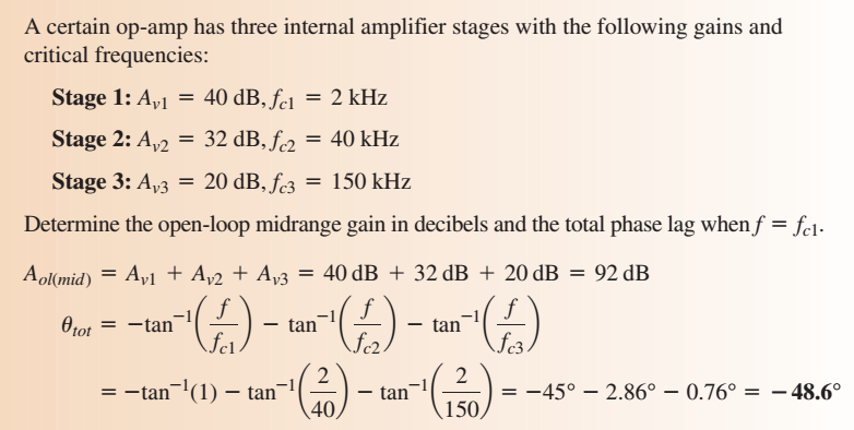
72 Bandwidth Limitations Frequency response of amplifiers is shown in a plot called Bode Plot. In Bode plot, the frequency is on the horizontal axis and is in logarithmic scale. It means that the frequency change is not linear but ten-times. This ten-time change in frequency is called a decade. The vertical axis shows the voltage gain in decibel (db). The maximum gain on the plot is called the midrange gain. The point in the frequency response of amplifiers where the gain is 3dB less than the midrange gain is called the critical frequency.
73 Bandwidth Limitations A ol (db) Midrange db/decade roll-off Critical frequency Unity-gain frequency (f T ) k 10k 100k 1M f (Hz)
74 Bandwidth Limitations An open-loop response curve (Bode plot) for a certain op-amp is shown. The differential open-loop gain A ol of an op amp is not infinite; rather, it is finite and decreases with frequency. Note that although the gain is quite high at dc and low frequencies, it starts to fall off at a rather low frequency. The process of modifying the open-loop gain is termed frequency compensation, and its purpose is to ensure that opamp circuits will be stable (as opposed to oscillatory). These are units that have a network (usually a single capacitor) included within the same IC chip whose function is to cause the op-amp gain to have the single-time-constant low-pass response shown.
75 Gain-Versus-Frequency Analysis The RC lag (low-pass) circuits within an op-amp are responsible for the roll-off in gain as the frequency increases, just as for the discrete amplifiers. The attenuation of an RC lag circuit shown is expressed as: The critical frequency of an RC circuit is:

76 Gain-Versus-Frequency Analysis If an op-amp is represented by a voltage gain element with a gain of A ol(mid) plus a single RC lag circuit, as shown, it is known as a compensated op-amp. The total open-loop gain of the op-amp is the product of the midrange open-loop gain, A ol(mid), and the attenuation of the RC circuit as:

77
78 Phase Shift An RC circuit causes a propagation delay from input to output, thus creating a phase shift between the input signal and the output signal. An RC lag circuit such as found in an op-amp stage causes the output signal voltage to lag the input. The phase shift, θ, is given by:

79
80 Overall Frequency Response Most op-amps have a constant roll-off of -20 db/decade above its critical frequency. The more complex IC operational amplifier may consist of two or more cascaded amplifier stages. The gain of each stage is frequency dependent and rolls off at above its critical frequency. Therefore, the total response of an op-amp is a composite of the individual responses of the internal stages. db gains are added and phase lags of the stages are added as shown in next slide for a three stage op-amp.
81
82
83 closed-loop frequency response Op-amps are usually used in a closed-loop configuration with negative feedback in order to achieve precise control of gain and bandwidth. Midrange gain of an op-amp is reduced by negative feedback as we have already seen in previous sections. Now we will see its effects on bandwidth.
84 Effect of Negative Feedback on Bandwidth The closed-loop critical frequency of an op-amp is given by: ff cc(cccc) = ff cc ooll (1 + BBAA oooo mmmmmm ) Where B is the feedback attenuation of the closed-loop op-amp. The above expression shows that the closed-loop critical frequency, ff cc(cccc), is higher than the open-loop critical frequency ff cc oooo by a factor of (1 + BBAA oooo mmmmmm ) Since ff cc(cccc) equals bandwidth therefore the closed-loop bandwidth, BBBB cccc, is also increased: BBBB cccc = BBBB ooll (1 + BBAA oooo mmmmmm )
85 Summary Bandwidth Limitations The Figure shows the concept of closed-loop response. When the openloop gain is reduced due to negative feedback, the bandwidth is increased. A v Open-loop gain This means that you can achieve a higher BW by accepting less gain. A ol(mid) A cl(mid) Closed-loop gain 0 f c(ol) f c(cl ) f
86 Gain-Bandwidth Product An increase in the closed-loop gain causes a decrease in the bandwidth and vice versa, such that the product of gain and bandwidth is constant. If AA cccc is the gain of an op-amp with ff cc(cccc) bandwidth then: AA cccc ff cc(cccc) = AA ooll ff cc(ooll) The equation, A cl f c(cl) = A ol f c(ol) shows that the product of the gain and bandwidth are constant. The gain-bandwidth product is always equal to the frequency at which the op-amp s open-loop gain is unity or 0 db (unity gain bandwidth, ff TT ) ff TT = AA cccc ff cc(cccc)
87 Example Determine the bandwidth of each of the amplifiers shown. Both op-amps have an open-loop gain of 100 db and a unitygain bandwidth (f T ) of 3 MHz.
88 Solution
89 Selected Key Terms Operational A type of amplifier that has very high voltage amplifier gain, very high input impedance, very low output impedance and good rejection of common-mode signals. Differential A mode of op-amp operation in which two mode opposite-polarity signals voltages are applied to the two inputs (double-ended) or in which a signal is applied to one input and ground to the other input (single-ended). Common mode A condition characterized by the presence of the same signal on both inputs
90 Selected Key Terms Open-loop The voltage gain of an op-amp without external voltage gain feedback. Negative The process of returning a portion of the output feedback signal to the input of an amplifier such that it is out of phase with the input. Closed-loop The voltage gain of an op-amp with external voltage gain feedback. Gainbandwidth the frequency at which the op-amp s open-loop A constant parameter which is always equal to product gain is unity (1).
91 Quiz 1. The ideal op-amp has a. zero input impedance and zero output impedance b. zero input impedance and infinite output impedance c. infinite input impedance and zero output impedance d. infinite input impedance and infinite output impedance
92 Quiz 2. The type of signal represented in the figure is a a. single-ended common-mode signal b. single-ended differential signal c. double-ended common-mode signal d. double-ended differential signal V in + V out
93 Quiz 3. CMRR can be expressed in a. amps b. volts c. ohms d. none of the above
94 Quiz 4. The difference in the two dc currents required to bias the differential amplifier in an op-amp is called the a. differential bias current b. input offset current c. input bias current d. none of the above
95 Quiz 5. To measure the slew rate of an op-amp, the input signal is a a. pulse b. triangle wave c. sine wave d. none of the above
96 Quiz 6. The input impedance of a noninverting amplifier is a. nearly 0 ohms b. approximately equal to R i c. approximately equal to R f d. extremely large
97 Quiz 7. The noninverting amplifier has a gain of 11. Assume that V in = 1.0 V. The approximate value of V f is a. 0 V b. 100 mv c. 1.0 V V in V f + R f 10 kω V out d. 11 V R i 1.0 kω
98 Quiz 8. The inverting amplifier has a gain of 10. Assume that V in = 1.0 V. The approximate value of the voltage at the inverting terminal of the op-amp is a. 0 V R f b. 100 mv c. 1.0 V d. 10 V V in R i 1.0 kω + 10 kω V out
99 Quiz 9. To compensate for bias current, the value of R c should be equal to a. R i R f b. R f c. R i R f R i V out d. R i + R f V in + R c
100 Quiz 10. Given a noninverting amplifier with a gain of 10 and a gain-bandwidth product of 1.0 MHz, the expected high critical frequency is a. 100 Hz b. 1.0 khz c. 10 khz d. 100 khz
101 Quiz Answers: 1. c 6. d 2. d 7. c 3. d 8. a 4. b 9. c 5. a 10. d
Chapter 12: The Operational Amplifier
 Chapter 12: The Operational Amplifier 12.1: Introduction to Operational Amplifier (Op-Amp) Operational amplifiers (op-amps) are very high gain dc coupled amplifiers with differential inputs; they are used
Reading: HH Sections 4.11 4.13, 4.19 4.20 (pgs. 189-212, 222 224)
") 6 OP AMPS II 6 Op Amps II In the previous lab, you explored several applications of op amps. In this exercise, you will look at some of their limitations. You will also examine the op amp integrator and
6 OP AMPS II 6 Op Amps II In the previous lab, you explored several applications of op amps. In this exercise, you will look at some of their limitations. You will also examine the op amp integrator and
Precision Diode Rectifiers
 by Kenneth A. Kuhn March 21, 2013 Precision half-wave rectifiers An operational amplifier can be used to linearize a non-linear function such as the transfer function of a semiconductor diode. The classic
Chapter 19 Operational Amplifiers
 Chapter 19 Operational Amplifiers The operational amplifier, or op-amp, is a basic building block of modern electronics. Op-amps date back to the early days of vacuum tubes, but they only became common
LM 358 Op Amp. If you have small signals and need a more useful reading we could amplify it using the op amp, this is commonly used in sensors.
 LM 358 Op Amp S k i l l L e v e l : I n t e r m e d i a t e OVERVIEW The LM 358 is a duel single supply operational amplifier. As it is a single supply it eliminates the need for a duel power supply, thus
Frequency Response of Filters
 School of Engineering Department of Electrical and Computer Engineering 332:224 Principles of Electrical Engineering II Laboratory Experiment 2 Frequency Response of Filters 1 Introduction Objectives To
OPERATIONAL AMPLIFIERS. o/p
 OPERATIONAL AMPLIFIERS 1. If the input to the circuit of figure is a sine wave the output will be i/p o/p a. A half wave rectified sine wave b. A fullwave rectified sine wave c. A triangular wave d. A
Use and Application of Output Limiting Amplifiers (HFA1115, HFA1130, HFA1135)
") Use and Application of Output Limiting Amplifiers (HFA111, HFA110, HFA11) Application Note November 1996 AN96 Introduction Amplifiers with internal voltage clamps, also known as limiting amplifiers, have
Use and Application of Output Limiting Amplifiers (HFA111, HFA110, HFA11) Application Note November 1996 AN96 Introduction Amplifiers with internal voltage clamps, also known as limiting amplifiers, have
Basic Op Amp Circuits
 Basic Op Amp ircuits Manuel Toledo INEL 5205 Instrumentation August 3, 2008 Introduction The operational amplifier (op amp or OA for short) is perhaps the most important building block for the design of
Op-Amp Simulation EE/CS 5720/6720. Read Chapter 5 in Johns & Martin before you begin this assignment.
 Op-Amp Simulation EE/CS 5720/6720 Read Chapter 5 in Johns & Martin before you begin this assignment. This assignment will take you through the simulation and basic characterization of a simple operational
Operational Amplifier - IC 741
 Operational Amplifier - IC 741 Tabish December 2005 Aim: To study the working of an 741 operational amplifier by conducting the following experiments: (a) Input bias current measurement (b) Input offset
Lab #9: AC Steady State Analysis
 Theory & Introduction Lab #9: AC Steady State Analysis Goals for Lab #9 The main goal for lab 9 is to make the students familar with AC steady state analysis, db scale and the NI ELVIS frequency analyzer.
Fig. 1 :Block diagram symbol of the operational amplifier. Characteristics ideal op-amp real op-amp
 Experiment: General Description An operational amplifier (op-amp) is defined to be a high gain differential amplifier. When using the op-amp with other mainly passive elements, op-amp circuits with various
School of Engineering Department of Electrical and Computer Engineering
 1 School of Engineering Department of Electrical and Computer Engineering 332:223 Principles of Electrical Engineering I Laboratory Experiment #4 Title: Operational Amplifiers 1 Introduction Objectives
OPERATIONAL AMPLIFIER
 MODULE3 OPERATIONAL AMPLIFIER Contents 1. INTRODUCTION... 3 2. Operational Amplifier Block Diagram... 3 3. Operational Amplifier Characteristics... 3 4. Operational Amplifier Package... 4 4.1 Op Amp Pins
Transistor Characteristics and Single Transistor Amplifier Sept. 8, 1997
 Physics 623 Transistor Characteristics and Single Transistor Amplifier Sept. 8, 1997 1 Purpose To measure and understand the common emitter transistor characteristic curves. To use the base current gain
Bipolar Transistor Amplifiers
 Physics 3330 Experiment #7 Fall 2005 Bipolar Transistor Amplifiers Purpose The aim of this experiment is to construct a bipolar transistor amplifier with a voltage gain of minus 25. The amplifier must
PIN CONFIGURATION FEATURES ORDERING INFORMATION ABSOLUTE MAXIMUM RATINGS. D, F, N Packages
 DESCRIPTION The µa71 is a high performance operational amplifier with high open-loop gain, internal compensation, high common mode range and exceptional temperature stability. The µa71 is short-circuit-protected
Current vs. Voltage Feedback Amplifiers
 Current vs. ltage Feedback Amplifiers One question continuously troubles the analog design engineer: Which amplifier topology is better for my application, current feedback or voltage feedback? In most
LABORATORY 2 THE DIFFERENTIAL AMPLIFIER
 LABORATORY 2 THE DIFFERENTIAL AMPLIFIER OBJECTIVES 1. To understand how to amplify weak (small) signals in the presence of noise. 1. To understand how a differential amplifier rejects noise and common
Building the AMP Amplifier
 Building the AMP Amplifier Introduction For about 80 years it has been possible to amplify voltage differences and to increase the associated power, first with vacuum tubes using electrons from a hot filament;
MAS.836 HOW TO BIAS AN OP-AMP
 MAS.836 HOW TO BIAS AN OP-AMP Op-Amp Circuits: Bias, in an electronic circuit, describes the steady state operating characteristics with no signal being applied. In an op-amp circuit, the operating characteristic
Operational Amplifiers
 Module 6 Amplifiers Operational Amplifiers The Ideal Amplifier What you ll learn in Module 6. Section 6.0. Introduction to Operational Amplifiers. Understand Concept of the Ideal Amplifier and the Need
www.jameco.com 1-800-831-4242
 Distributed by: www.jameco.com 1-800-831-4242 The content and copyrights of the attached material are the property of its owner. LF411 Low Offset, Low Drift JFET Input Operational Amplifier General Description
Physics 623 Transistor Characteristics and Single Transistor Amplifier Sept. 13, 2006
 Physics 623 Transistor Characteristics and Single Transistor Amplifier Sept. 13, 2006 1 Purpose To measure and understand the common emitter transistor characteristic curves. To use the base current gain
Electronics. Discrete assembly of an operational amplifier as a transistor circuit. LD Physics Leaflets P4.2.1.1
 Electronics Operational Amplifier Internal design of an operational amplifier LD Physics Leaflets Discrete assembly of an operational amplifier as a transistor circuit P4.2.1.1 Objects of the experiment
TS321 Low Power Single Operational Amplifier
 SOT-25 Pin Definition: 1. Input + 2. Ground 3. Input - 4. Output 5. Vcc General Description The TS321 brings performance and economy to low power systems. With high unity gain frequency and a guaranteed
TL074 TL074A - TL074B
 A B LOW NOISE JFET QUAD OPERATIONAL AMPLIFIERS WIDE COMMONMODE (UP TO V + CC ) AND DIFFERENTIAL VOLTAGE RANGE LOW INPUT BIAS AND OFFSET CURRENT LOW NOISE e n = 15nV/ Hz (typ) OUTPUT SHORTCIRCUIT PROTECTION
Transistor Amplifiers
 Physics 3330 Experiment #7 Fall 1999 Transistor Amplifiers Purpose The aim of this experiment is to develop a bipolar transistor amplifier with a voltage gain of minus 25. The amplifier must accept input
Lab 7: Operational Amplifiers Part I
 Lab 7: Operational Amplifiers Part I Objectives The objective of this lab is to study operational amplifier (op amp) and its applications. We will be simulating and building some basic op amp circuits,
11: AUDIO AMPLIFIER I. INTRODUCTION
 11: AUDIO AMPLIFIER I. INTRODUCTION The properties of an amplifying circuit using an op-amp depend primarily on the characteristics of the feedback network rather than on those of the op-amp itself. A
Programmable-Gain Transimpedance Amplifiers Maximize Dynamic Range in Spectroscopy Systems
 Programmable-Gain Transimpedance Amplifiers Maximize Dynamic Range in Spectroscopy Systems PHOTODIODE VOLTAGE SHORT-CIRCUIT PHOTODIODE SHORT- CIRCUIT VOLTAGE 0mV DARK ark By Luis Orozco Introduction Precision
Fully Differential CMOS Amplifier
 ECE 511 Analog Electronics Term Project Fully Differential CMOS Amplifier Saket Vora 6 December 2006 Dr. Kevin Gard NC State University 1 Introduction In this project, a fully differential CMOS operational
Laboratory 4: Feedback and Compensation
 Laboratory 4: Feedback and Compensation To be performed during Week 9 (Oct. 20-24) and Week 10 (Oct. 27-31) Due Week 11 (Nov. 3-7) 1 Pre-Lab This Pre-Lab should be completed before attending your regular
Objectives The purpose of this lab is build and analyze Differential amplifiers based on NPN transistors (or NMOS transistors).
.") 1 Lab 03: Differential Amplifiers (BJT) (20 points) NOTE: 1) Please use the basic current mirror from Lab01 for the second part of the lab (Fig. 3). 2) You can use the same chip as the basic current mirror;
1 Lab 03: Differential Amplifiers (BJT) (20 points) NOTE: 1) Please use the basic current mirror from Lab01 for the second part of the lab (Fig. 3). 2) You can use the same chip as the basic current mirror;
Homework Assignment 03
 Question 1 (2 points each unless noted otherwise) Homework Assignment 03 1. A 9-V dc power supply generates 10 W in a resistor. What peak-to-peak amplitude should an ac source have to generate the same
Technical Note #3. Error Amplifier Design and Applications. Introduction
 Technical Note #3 Error Amplifier Design and Applications Introduction All regulating power supplies require some sort of closed-loop control to force the output to match the desired value. Both digital
TL082 Wide Bandwidth Dual JFET Input Operational Amplifier
 TL082 Wide Bandwidth Dual JFET Input Operational Amplifier General Description These devices are low cost high speed dual JFET input operational amplifiers with an internally trimmed input offset voltage
Description. 5k (10k) - + 5k (10k)
 - + 5k (10k)") THAT Corporation Low Noise, High Performance Microphone Preamplifier IC FEATURES Excellent noise performance through the entire gain range Exceptionally low THD+N over the full audio bandwidth Low power
THAT Corporation Low Noise, High Performance Microphone Preamplifier IC FEATURES Excellent noise performance through the entire gain range Exceptionally low THD+N over the full audio bandwidth Low power
6.101 Final Project Report Class G Audio Amplifier
 6.101 Final Project Report Class G Audio Amplifier Mark Spatz 4/3/2014 1 1 Introduction For my final project, I designed and built a 150 Watt audio amplifier to replace the underpowered and unreliable
Description. Output Stage. 5k (10k) - + 5k (10k)
 - + 5k (10k)") THAT Corporation Low Noise, High Performance Audio Preamplifier IC FEATURES Low Noise: 1 nv/hz input noise (60dB gain) 34 nv/hz input noise (0dB gain) (1512) Low THD+N (full audio bandwidth): 0.0005% 40dB
THAT Corporation Low Noise, High Performance Audio Preamplifier IC FEATURES Low Noise: 1 nv/hz input noise (60dB gain) 34 nv/hz input noise (0dB gain) (1512) Low THD+N (full audio bandwidth): 0.0005% 40dB
Analog Signal Conditioning
 Analog Signal Conditioning Analog and Digital Electronics Electronics Digital Electronics Analog Electronics 2 Analog Electronics Analog Electronics Operational Amplifiers Transistors TRIAC 741 LF351 TL084
Digital to Analog Converter. Raghu Tumati
 Digital to Analog Converter Raghu Tumati May 11, 2006 Contents 1) Introduction............................... 3 2) DAC types................................... 4 3) DAC Presented.............................
Positive Feedback and Oscillators
 Physics 3330 Experiment #6 Fall 1999 Positive Feedback and Oscillators Purpose In this experiment we will study how spontaneous oscillations may be caused by positive feedback. You will construct an active
TDA2040. 20W Hi-Fi AUDIO POWER AMPLIFIER
 20W Hi-Fi AUDIO POWER AMPLIFIER DESCRIPTION The TDA2040 is a monolithic integrated circuit in Pentawatt package, intended for use as an audio class AB amplifier. Typically it provides 22W output power
LAB 12: ACTIVE FILTERS
 A. INTRODUCTION LAB 12: ACTIVE FILTERS After last week s encounter with op- amps we will use them to build active filters. B. ABOUT FILTERS An electric filter is a frequency-selecting circuit designed
Op amp DC error characteristics and the effect on high-precision applications
 Op amp DC error characteristics and the effect on high-precision applications Srudeep Patil, Member of Technical Staff, Maxim Integrated - January 01, 2014 This article discusses the DC limitations of
TL084 TL084A - TL084B
 A B GENERAL PURPOSE JFET QUAD OPERATIONAL AMPLIFIERS WIDE COMMONMODE (UP TO V + CC ) AND DIFFERENTIAL VOLTAGE RANGE LOW INPUT BIAS AND OFFSET CURRENT OUTPUT SHORTCIRCUIT PROTECTION HIGH INPUT IMPEDANCE
How To Calculate The Power Gain Of An Opamp
 A. M. Niknejad University of California, Berkeley EE 100 / 42 Lecture 8 p. 1/23 EE 42/100 Lecture 8: Op-Amps ELECTRONICS Rev C 2/8/2012 (9:54 AM) Prof. Ali M. Niknejad University of California, Berkeley
CIRCUITS LABORATORY EXPERIMENT 3. AC Circuit Analysis
 CIRCUITS LABORATORY EXPERIMENT 3 AC Circuit Analysis 3.1 Introduction The steady-state behavior of circuits energized by sinusoidal sources is an important area of study for several reasons. First, the
APPLICATION BULLETIN
 APPLICATION BULLETIN Mailing Address: PO Box 11400, Tucson, AZ 85734 Street Address: 6730 S. Tucson Blvd., Tucson, AZ 85706 Tel: (520) 746-1111 Telex: 066-6491 FAX (520) 889-1510 Product Info: (800) 548-6132
High Common-Mode Rejection. Differential Line Receiver SSM2141. Fax: 781/461-3113 FUNCTIONAL BLOCK DIAGRAM FEATURES. High Common-Mode Rejection
 a FEATURES High Common-Mode Rejection DC: 00 db typ 60 Hz: 00 db typ 20 khz: 70 db typ 40 khz: 62 db typ Low Distortion: 0.00% typ Fast Slew Rate: 9.5 V/ s typ Wide Bandwidth: 3 MHz typ Low Cost Complements
5B5BBasic RC Oscillator Circuit
 5B5BBasic RC Oscillator Circuit The RC Oscillator which is also called a Phase Shift Oscillator, produces a sine wave output signal using regenerative feedback from the resistor-capacitor combination.
A Low-Cost VCA Limiter
 The circuits within this application note feature THAT218x to provide the essential function of voltage-controlled amplifier (VCA). Since writing this note, THAT has introduced a new dual VCA, as well
Differential Amplifier Offset. Causes of dc voltage and current offset Modeling dc offset R C
 ESE39 ntroduction to Microelectronics Differential Amplifier Offset Causes of dc voltage and current offset Modeling dc offset mismatch S mismatch β mismatch transistor mismatch dc offsets in differential
Basic Electronics Prof. Dr. Chitralekha Mahanta Department of Electronics and Communication Engineering Indian Institute of Technology, Guwahati
 Basic Electronics Prof. Dr. Chitralekha Mahanta Department of Electronics and Communication Engineering Indian Institute of Technology, Guwahati Module: 2 Bipolar Junction Transistors Lecture-2 Transistor
OBJECTIVE QUESTIONS IN ANALOG ELECTRONICS
 1. The early effect in a bipolar junction transistor is caused by (a) fast turn-on (c) large collector-base reverse bias (b)fast turn-off (d) large emitter-base forward bias 2. MOSFET can be used as a
LM118/LM218/LM318 Operational Amplifiers
 LM118/LM218/LM318 Operational Amplifiers General Description The LM118 series are precision high speed operational amplifiers designed for applications requiring wide bandwidth and high slew rate. They
Scaling and Biasing Analog Signals
 Scaling and Biasing Analog Signals November 2007 Introduction Scaling and biasing the range and offset of analog signals is a useful skill for working with a variety of electronics. Not only can it interface
AC 2012-3923: MEASUREMENT OF OP-AMP PARAMETERS USING VEC- TOR SIGNAL ANALYZERS IN UNDERGRADUATE LINEAR CIRCUITS LABORATORY
 AC 212-3923: MEASUREMENT OF OP-AMP PARAMETERS USING VEC- TOR SIGNAL ANALYZERS IN UNDERGRADUATE LINEAR CIRCUITS LABORATORY Dr. Tooran Emami, U.S. Coast Guard Academy Tooran Emami received her M.S. and Ph.D.
LM833 LOW NOISE DUAL OPERATIONAL AMPLIFIER
 LOW NOISE DUAL OPERATIONAL AMPLIFIER LOW VOLTAGE NOISE: 4.5nV/ Hz HIGH GAIN BANDWIDTH PRODUCT: 15MHz HIGH SLEW RATE: 7V/µs LOW DISTORTION:.2% EXCELLENT FREQUENCY STABILITY ESD PROTECTION 2kV DESCRIPTION
TDA2040. 20W Hi-Fi AUDIO POWER AMPLIFIER
 20W Hi-Fi AUDIO POWER AMPLIFIER DESCRIPTION The TDA2040 is a monolithic integrated circuit in Pentawatt package, intended for use as an audio class AB amplifier. Typically it provides 22W output power
AVR127: Understanding ADC Parameters. Introduction. Features. Atmel 8-bit and 32-bit Microcontrollers APPLICATION NOTE
 Atmel 8-bit and 32-bit Microcontrollers AVR127: Understanding ADC Parameters APPLICATION NOTE Introduction This application note explains the basic concepts of analog-to-digital converter (ADC) and the
WHY DIFFERENTIAL? instruments connected to the circuit under test and results in V COMMON.
 WHY DIFFERENTIAL? Voltage, The Difference Whether aware of it or not, a person using an oscilloscope to make any voltage measurement is actually making a differential voltage measurement. By definition,
PowerAmp Design. PowerAmp Design PAD135 COMPACT HIGH VOLATGE OP AMP
 PowerAmp Design COMPACT HIGH VOLTAGE OP AMP Rev G KEY FEATURES LOW COST SMALL SIZE 40mm SQUARE HIGH VOLTAGE 200 VOLTS HIGH OUTPUT CURRENT 10A PEAK 40 WATT DISSIPATION CAPABILITY 200V/µS SLEW RATE APPLICATIONS
Op Amp Circuit Collection
 Op Amp Circuit Collection Note: National Semiconductor recommends replacing 2N2920 and 2N3728 matched pairs with LM394 in all application circuits. Section 1 Basic Circuits Inverting Amplifier Difference
LF412 Low Offset Low Drift Dual JFET Input Operational Amplifier
 LF412 Low Offset Low Drift Dual JFET Input Operational Amplifier General Description These devices are low cost high speed JFET input operational amplifiers with very low input offset voltage and guaranteed
Common Emitter BJT Amplifier Design Current Mirror Design
 Common Emitter BJT Amplifier Design Current Mirror Design 1 Some Random Observations Conditions for stabilized voltage source biasing Emitter resistance, R E, is needed. Base voltage source will have finite
High Speed, Low Power Monolithic Op Amp AD847
 a FEATURES Superior Performance High Unity Gain BW: MHz Low Supply Current:.3 ma High Slew Rate: 3 V/ s Excellent Video Specifications.% Differential Gain (NTSC and PAL).9 Differential Phase (NTSC and
EXPERIMENT NUMBER 5 BASIC OSCILLOSCOPE OPERATIONS
 1 EXPERIMENT NUMBER 5 BASIC OSCILLOSCOPE OPERATIONS The oscilloscope is the most versatile and most important tool in this lab and is probably the best tool an electrical engineer uses. This outline guides
Making Accurate Voltage Noise and Current Noise Measurements on Operational Amplifiers Down to 0.1Hz
 Author: Don LaFontaine Making Accurate Voltage Noise and Current Noise Measurements on Operational Amplifiers Down to 0.1Hz Abstract Making accurate voltage and current noise measurements on op amps in
CHAPTER 10 OPERATIONAL-AMPLIFIER CIRCUITS
 CHAPTER 10 OPERATIONAL-AMPLIFIER CIRCUITS Chapter Outline 10.1 The Two-Stage CMOS Op Amp 10.2 The Folded-Cascode CMOS Op Amp 10.3 The 741 Op-Amp Circuit 10.4 DC Analysis of the 741 10.5 Small-Signal Analysis
LH0091 True RMS to DC Converter
 LH0091 True RMS to DC Converter General Description The LH0091 rms to dc converter generates a dc output equal to the rms value of any input per the transfer function E OUT(DC) e 0 1 T T 0 E IN 2 (t) dt
Understanding Power Impedance Supply for Optimum Decoupling
 Introduction Noise in power supplies is not only caused by the power supply itself, but also the load s interaction with the power supply (i.e. dynamic loads, switching, etc.). To lower load induced noise,
Application Report SLVA051
 Application Report November 998 Mixed-Signal Products SLVA05 ltage Feedback Vs Current Feedback Op Amps Application Report James Karki Literature Number: SLVA05 November 998 Printed on Recycled Paper IMPORTANT
LF442 Dual Low Power JFET Input Operational Amplifier
 LF442 Dual Low Power JFET Input Operational Amplifier General Description The LF442 dual low power operational amplifiers provide many of the same AC characteristics as the industry standard LM1458 while
GenTech Practice Questions
 GenTech Practice Questions Basic Electronics Test: This test will assess your knowledge of and ability to apply the principles of Basic Electronics. This test is comprised of 90 questions in the following
ENEE 307 Electronic Circuit Design Laboratory Spring 2012. A. Iliadis Electrical Engineering Department University of Maryland College Park MD 20742
 1.1. Differential Amplifiers ENEE 307 Electronic Circuit Design Laboratory Spring 2012 A. Iliadis Electrical Engineering Department University of Maryland College Park MD 20742 Differential Amplifiers
PIEZO FILTERS INTRODUCTION
 For more than two decades, ceramic filter technology has been instrumental in the proliferation of solid state electronics. A view of the future reveals that even greater expectations will be placed on
LABORATORY MANUAL DEPARTMENT OF ELECTRICAL & COMPUTER ENGINEERING
 LABORATORY MANUAL DEPARTMENT OF ELECTRICAL & COMPUTER ENGINEERING UNIVERSITY OF CENTRAL FLORIDA EEL 4309 Electronics II Revised January 2012 Table of Contents Safety: Introduction: Experiment #1: Experiment
Application Note 142 August 2013. New Linear Regulators Solve Old Problems AN142-1
 August 2013 New Linear Regulators Solve Old Problems Bob Dobkin, Vice President, Engineering and CTO, Linear Technology Corp. Regulators regulate but are capable of doing much more. The architecture of
Design of a TL431-Based Controller for a Flyback Converter
 Design of a TL431-Based Controller for a Flyback Converter Dr. John Schönberger Plexim GmbH Technoparkstrasse 1 8005 Zürich 1 Introduction The TL431 is a reference voltage source that is commonly used
Wide Bandwidth, Fast Settling Difet OPERATIONAL AMPLIFIER
 Wide Bandwidth, Fast Settling Difet OPERATIONAL AMPLIFIER FEATURES HIGH GAIN-BANDWIDTH: 35MHz LOW INPUT NOISE: 1nV/ Hz HIGH SLEW RATE: V/µs FAST SETTLING: 24ns to.1% FET INPUT: I B = 5pA max HIGH OUTPUT
Precision, Unity-Gain Differential Amplifier AMP03
 a FEATURES High CMRR: db Typ Low Nonlinearity:.% Max Low Distortion:.% Typ Wide Bandwidth: MHz Typ Fast Slew Rate: 9.5 V/ s Typ Fast Settling (.%): s Typ Low Cost APPLICATIONS Summing Amplifiers Instrumentation
b 1 is the most significant bit (MSB) The MSB is the bit that has the most (largest) influence on the analog output
 The MSB is the bit that has the most (largest) influence on the analog output") CMOS Analog IC Design - Chapter 10 Page 10.0-5 BLOCK DIAGRAM OF A DIGITAL-ANALOG CONVERTER b 1 is the most significant bit (MSB) The MSB is the bit that has the most (largest) influence on the analog output
CMOS Analog IC Design - Chapter 10 Page 10.0-5 BLOCK DIAGRAM OF A DIGITAL-ANALOG CONVERTER b 1 is the most significant bit (MSB) The MSB is the bit that has the most (largest) influence on the analog output
Cancellation of Load-Regulation in Low Drop-Out Regulators
 Cancellation of Load-Regulation in Low Drop-Out Regulators Rajeev K. Dokania, Student Member, IEE and Gabriel A. Rincόn-Mora, Senior Member, IEEE Georgia Tech Analog Consortium Georgia Institute of Technology
Laboratory Manual. ELEN-325 Electronics
 Laboratory Manual ELEN-325 Electronics Department of Electrical & Computer Engineering Texas A&M University Prepared by: Dr. Jose Silva-Martinez ([email protected]) Rida Assaad ([email protected]) Raghavendra
Lecture - 4 Diode Rectifier Circuits
 Basic Electronics (Module 1 Semiconductor Diodes) Dr. Chitralekha Mahanta Department of Electronics and Communication Engineering Indian Institute of Technology, Guwahati Lecture - 4 Diode Rectifier Circuits
Diodes have an arrow showing the direction of the flow.
 The Big Idea Modern circuitry depends on much more than just resistors and capacitors. The circuits in your computer, cell phone, Ipod depend on circuit elements called diodes, inductors, transistors,
S-Parameters and Related Quantities Sam Wetterlin 10/20/09
 S-Parameters and Related Quantities Sam Wetterlin 10/20/09 Basic Concept of S-Parameters S-Parameters are a type of network parameter, based on the concept of scattering. The more familiar network parameters
Section 3. Sensor to ADC Design Example
 Section 3 Sensor to ADC Design Example 3-1 This section describes the design of a sensor to ADC system. The sensor measures temperature, and the measurement is interfaced into an ADC selected by the systems
APPLICATION NOTE ULTRASONIC CERAMIC TRANSDUCERS
 APPLICATION NOTE ULTRASONIC CERAMIC TRANSDUCERS Selection and use of Ultrasonic Ceramic Transducers The purpose of this application note is to aid the user in the selection and application of the Ultrasonic
Kit 106. 50 Watt Audio Amplifier
 Kit 106 50 Watt Audio Amplifier T his kit is based on an amazing IC amplifier module from ST Electronics, the TDA7294 It is intended for use as a high quality audio class AB amplifier in hi-fi applications
OPERATIONAL AMPLIFIERS
 INTRODUCTION OPERATIONAL AMPLIFIERS The student will be introduced to the application and analysis of operational amplifiers in this laboratory experiment. The student will apply circuit analysis techniques
The Operational Amplfier Lab Guide
 EECS 100 Lab Guide Bharathwaj Muthuswamy The Operational Amplfier Lab Guide 1. Introduction COMPONENTS REQUIRED FOR THIS LAB : 1. LM741 op-amp integrated circuit (IC) 2. 1k resistors 3. 10k resistor 4.
LM101A LM201A LM301A Operational Amplifiers
 LM101A LM201A LM301A Operational Amplifiers General Description The LM101A series are general purpose operational amplifiers which feature improved performance over industry standards like the LM709 Advanced
DIGITAL-TO-ANALOGUE AND ANALOGUE-TO-DIGITAL CONVERSION
 DIGITAL-TO-ANALOGUE AND ANALOGUE-TO-DIGITAL CONVERSION Introduction The outputs from sensors and communications receivers are analogue signals that have continuously varying amplitudes. In many systems
100V - 100W DMOS AUDIO AMPLIFIER WITH MUTE/ST-BY THERMAL SHUTDOWN STBY-GND
 TDA7294 100V - 100W DMOS AUDIO AMPLIFIER WITH MUTE/ST-BY VERY HIGH OPERATING VOLTAGE RANGE (±40V) DMOS POWER STAGE HIGH OUTPUT POWER (UP TO 100W MU- SIC POWER) MUTING/STAND-BY FUNCTIONS NO SWITCH ON/OFF
isim ACTIVE FILTER DESIGNER NEW, VERY CAPABLE, MULTI-STAGE ACTIVE FILTER DESIGN TOOL
 isim ACTIVE FILTER DESIGNER NEW, VERY CAPABLE, MULTI-STAGE ACTIVE FILTER DESIGN TOOL Michael Steffes Sr. Applications Manager 12/15/2010 SIMPLY SMARTER Introduction to the New Active Filter Designer Scope