View of ΣIGMA TM (Ref. 1)
|
|
|
- Dina Ford
- 10 years ago
- Views:
Transcription
1 Overview of the FESEM system 1. Electron optical column 2. Specimen chamber 3. EDS detector [Electron Dispersive Spectroscopy] 4. Monitors 5. BSD (Back scatter detector) 6. Personal Computer 7. ON/STANDBY/OFF button 8. Plinth 9. WDX (not in existing FESEM) [Wavelength Dispersive X ray analysis] View of ΣIGMA TM (Ref. 1)

2 Principle of operation 1. Gun with filament 2. Ion getter pump 3. Specimen chamber 4. Penning gauge 5. Pre vacuum pump 6. Turbo pump 7. Vent valve 8. Column chamber valve 9. Multi hole aperture 10. Gun head Schematic of vacuum system (Ref. 1) FESEM uses a focused beam of electrons to generate an image or to analyze the specimen. For operation, the gun head, the column and specimen chamber have to be evacuated. The pre vacuum pump and turbo pump evacuate the specimen chamber. Vacuum in the specimen chamber is measure by penning gauge. Column chamber valve remains closed until the detected pressure is not ready for operation. After vent command, column chamber valve closes and N 2 gas flows into the specimen chamber through vent valve.

3 Electron optics 1. Schottky field emitter 2. Anode 3. Multi hole aperture 4. Gun/aperture alignment system 5. Condenser lens 6. Stigmator 7. Linear tube 8. In lens detector 9. Objective lens 10. Scan coils and stigmator 11. Objective cap Schematic of vacuum system (See Ref. 1) Schottky emitter (1) emits electrons. The beam of electrons passes through anode (2) aperture. Electron beam passes through the multihole aperture (3). Standard aperture is 30 μm hole. Other aperture sizes can be selected by using the gun/aperture alignment system (4). Stigmator (6) makes sure the beam is rotationally symmetrical. Anode and linear tube (7) are connected to form the beam booster. Beam booster provides better protection against external stray fields. Condenser lens (5) controls the amount of demagnification. Objective lens focuses the electron beam onto the specimen. Objective lens consists of electromagnetic (8) and electrostatic (9) lens. Deflection system consists of a set of scan coils (10) to move the electron beam in a point to point scan process.
 makes sure the beam is rotationally symmetrical. Anode and linear tube (7) are connected to form the beam booster. Beam booster provides better protection against external stray fields.")
4 Control elements Example of SmartSEM user interface (Ref. 1)

5 ΣIGMA smartsem has three imaging modes. 1. In lens image mode 2. Secondary electron image mode (SE) 3. Backscattered electron image mode (BSE) Imaging modes Interaction between primary electron beam and sample (Ref. 1) Secondary electrons (SEs) have low energy. (less than 50 ev) The electrons with energy higher than 50 ev are known as backscattered electrons (BSEs)
 Secondary electrons (SEs) have low energy.")
6 In lens image mode To map the actual surface of a sample, secondary electrons of type (SE1) should be detected. In lens detector detects SE1 very efficiently as it is located in the beam path. The efficiency of in lens image depends on working distance (WD) which determines the S/N ratio. WD should be selected depending on the geometry of specimen and acceleration voltage in use. Benefits of In lens mode are: high detection efficiency In lens image mode (Ref. 1) pure detection of SE more surface information Clear edge effect In lens mode has limited applications because of small WD which limits smallest possible magnification A small spot can appear in the center of image at low magnification Only suitable in high vacuum and with acceleration voltages upto 20 kv. Refer pg 42 of Sigma user manual for in lens detector characteristics.
 pure detection of SE more surface information Clear edge effect In lens mode has limited applications because of small WD which limits smallest possible magnification A small spot can appear in")
7 SE image mode ET SE or Everhart Thornley, detector is mounted on the wall of the specimen chamber It allows detection of secondary electrons with a small backscattered component Working distance has significant effect on the efficiency of SE mode. For WD too short, shadowing effects occur. A minimum WD of approx. 4 mm should be used. ET SE detector is very good when used at long working distances. As SE detector is mounted at a certain angle to the specimen, the specimen is always viewed laterally. Therefore, it provides good surface information. Refer pg 52 of Sigma user manual for SE detector characteristics. SE image mode (Ref. 1)

8 BSE image mode The application of BSE image mode is to display compositional differences (material contrast) in the specimen. As the BSE detector is located below the final lens, it offers a large solid angle to detect backscattered electrons. The performance is based on backscattering coeff. Which increase with increasing atomic number. Factors affecting BSE efficiency The acceleration voltage Working distance Refer pg 56 of Sigma user manual for BSE detector characteristics. BSE image mode (Ref. 1)

9 Electron Lenses Electron lenses are used to demagnify the image of the beam crossover in the electron gun to the final spot size on the specimen. SEMs employ electromagnetic (EM) lenses because these lenses have smaller aberrations. Electron focusing EM lens consists of a coil of wire which generates a magnetic field across the lens gap between the polepieces. The distance from the point where an electron starts to bend towards the axis to the point where it crosses the axis is called the lens focal length f p q q Magnification M p Using two or three lenses to demagnify, one can reduce the probe size for a typical tungsten hairpin SEM to about 10 nm, excluding the effects of aberrations. Electron lens and their optics (Ref. 2)

10 Lenses in FESEM The electron beam is focused by the electro magnetic lenses, condenser lens and objective lens. Lenses in FESEM (Ref. 1) 5. Condenser lens Condenser lens controls the amount of demagnification. The current in the condenser determines the diameter of the beam: a low current results in a small diameter, a 9. Objective lens higher current in a larger beam. A narrow beam has the advantage that the resolution is better, but the disadvantage that the signal to noise ratio is worse. The situation is reversed when the beam has a large diameter. Objectivej lens focuses the electron beam onto the specimen. It is the lowest lens in the column. At a short working distance the objective lens needs to apply a greater force to deflect the electron beam. The shortest working distance produces the smallest beam diameter, the best resolution, but also the poorest depth of field.

11 Examples of FE electron guns (Ref. 2) Field Emission Guns Field emission is an alternative way of generating electrons. Field emitters are fine tungsten needles. Some field emitters are coated with low working function materials such as zirconium oxide. These types of field emitters are called Schottky emitters. Schottky and cold field emission are superior to thermionic i sources in terms of source size, brightness, and lifetime. ΣIGMA TM is equipped with Schottky field emitter (SFE). In the SFE, Zr0 2 is deposited on the flattened tip to enhance its brightness and emission density.re comparable with those of a CFE. SFE guns include a suppressor grid to eliminate unwanted thermionic emission from regions outside of tip. Useful life of a SFE is about months, so it must be replaced on a regular basis. Vacuum level required for successful Schottky operation is not as demanding as that for a CFE, but in practice an ultrahigh vacuum aids long term stability, prevents poisoning of the ZrO2 cathode, and maximizes brightness.

12 Lens Aberrations In an ideal optical system, all rays of light from a point in the object plane would converge to the same point in the image plane, forming a clear image. The influences which cause different rays to converge to different points are called aberrations Spherical Aberration Spherical aberration arises because electrons are bent more strongly by the lens magnetic field than those rays near the axis. This results in a disk rather than a point where all rays converge. The smallest disk occurs just in front of the Gaussian plane and is called the spherical aberration disk of least confusion. Spherical Aberration (Ref. 2) Aperture diffraction For very small apertures, the wave nature of electrons gives rise to a circular diffraction pattern instead of a point at the Gaussian image plane. Spherical aberration and aperture diffraction in a lens cause a point object at P to blur into an enlarged spot at the Gaussian image plane. The disk of minimum confusion d s and one half the Airy disk d d are used in calculations of probe size. Aperture diffraction (Ref. 2)

13 Lens Aberrations Chromatic Aberration Electrons of different energy are focused at different locations The chromatic disk of minimum confusion d c is only important at low accelerating voltages Astigmatism Astigmatism occurs when the electrons sense a nonuniform magnetic field as they spiral around the optic axis. Machining errors, inhomogeneities in the polepieces, asymmetry in the lens windings, and dirty apertures all may lead to a lens that is not perfectly cylindrical, but is "astigmatic. This means that a point object P will produce two separate line foci at the image and the desired small focused beam can only be obtained by forcing the two line foci to coincide using the stigmator. The effect can be corrected using the stigmator, that applies a supplement magnetic field to make the lens appear symmetric to electron beam.

14 Lens Aberrations All lenses suffer from a number of defects oraberrations in their performance. However, in electron optics, by contrast to the situation in light optics, the effects of aberrations cannot be canceled by using combinations of lenses. The only recourse therefore is to try to minimize these effects. The effects of the aberrations are most significant in the objective lens because the amount of blurring these aberrations cause in the preceding lenses is small relative to the larger size of the beam at those lenses. Astigmatism can be completely corrected in the final lens of a properly maintained SEM. The effects of spherical aberration and aperture diffraction remain to be controlled at normal accelerating voltages of kv. Chromatic aberration begins to seriously degrade the image at accelerating voltages under 10 kv.

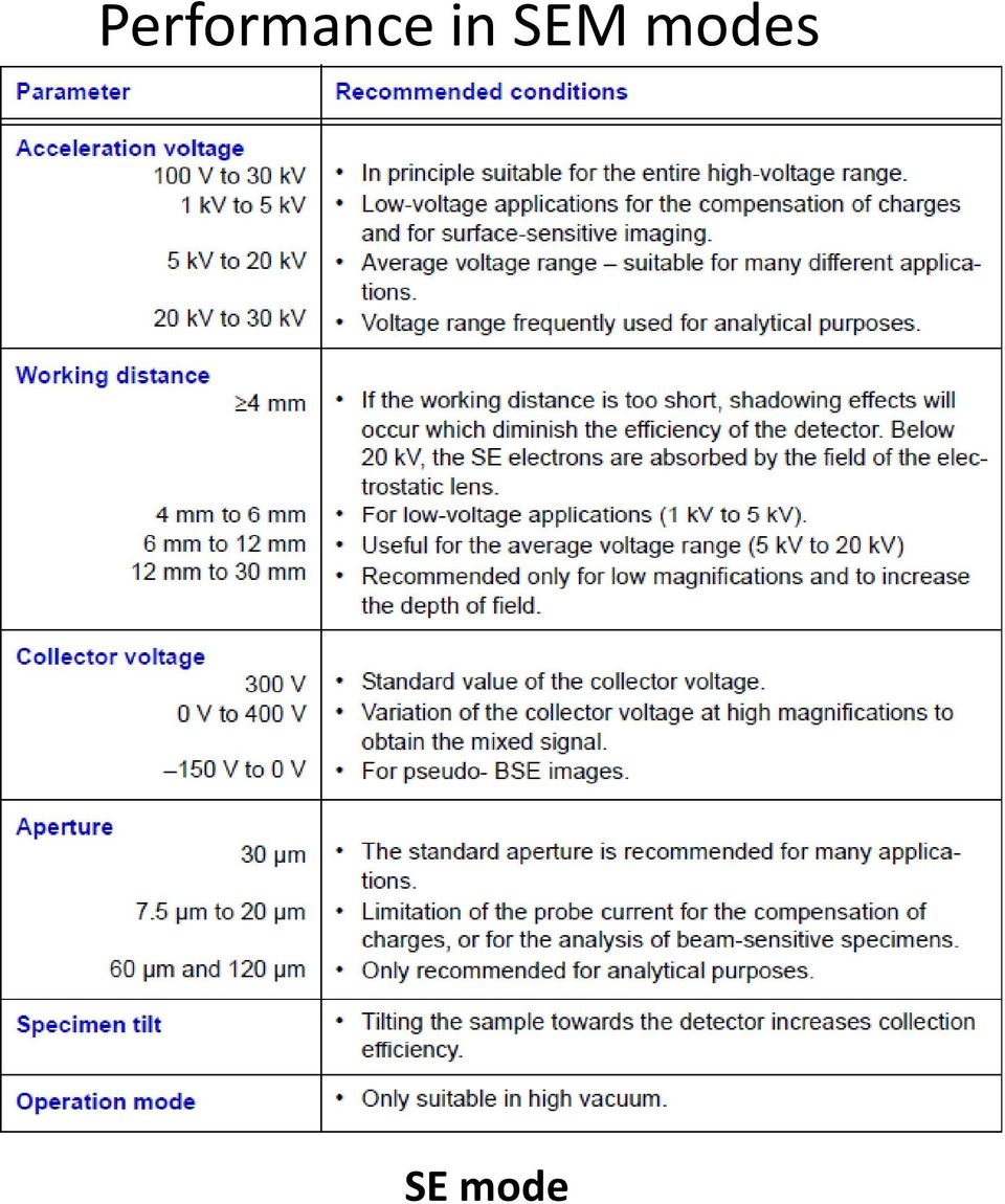
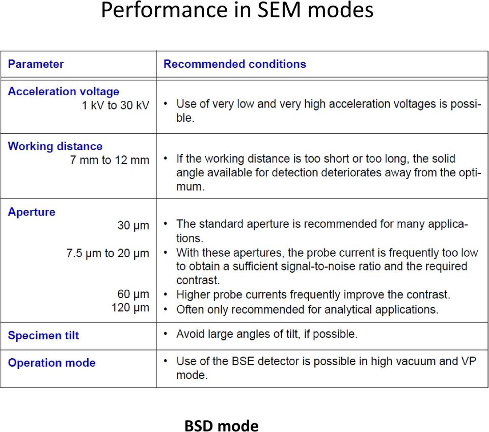
15 Performance in SEM modes SEM operators should know the actual electron beam parameters for the SEM that they are operating. The charts of values of various accelerating voltages, working distances and aperture sizes for three imaging modes of ΣIGMA TM is provided by manufacturer. In lens mode

16 Performance in SEM modes SE mode
17 Performance in SEM modes BSD mode
18 References 1. ΣIGMA FESEM Operator s user guide en02, April Joseph Goldstein et. al., Scanning Electron Microscopy and X ray microanalysis, Kluwer Academic/Plenum Publishers, New York, 2003.

Scanning Electron Microscopy Primer
 Scanning Electron Microscopy Primer Bob Hafner This primer is intended as background for the Introductory Scanning Electron Microscopy training offered by the University of Minnesota s Characterization
The Basics of Scanning Electron Microscopy
 The Basics of Scanning Electron Microscopy The small scanning electron microscope is easy to use because almost every variable is pre-set: the acceleration voltage is always 15kV, it has only a single
Name: Due: September 21 st 2012. Physics 7230 Laboratory 3: High Resolution SEM Imaging
 Name: Due: September 21 st 2012 Physics 7230 Laboratory 3: High Resolution SEM Imaging 1. What is meant by the term resolution? How does this differ from other image variables, such as signal to noise
Lenses and Apertures of A TEM
 Instructor: Dr. C.Wang EMA 6518 Course Presentation Lenses and Apertures of A TEM Group Member: Anup Kr. Keshri Srikanth Korla Sushma Amruthaluri Venkata Pasumarthi Xudong Chen Outline Electron Optics
Preface Light Microscopy X-ray Diffraction Methods
 Preface xi 1 Light Microscopy 1 1.1 Optical Principles 1 1.1.1 Image Formation 1 1.1.2 Resolution 3 1.1.3 Depth of Field 5 1.1.4 Aberrations 6 1.2 Instrumentation 8 1.2.1 Illumination System 9 1.2.2 Objective
Fundamentals of Scanning Electron Microscopy
 1 Fundamentals of Scanning Electron Microscopy Weilie Zhou, Robert P. Apkarian, Zhong Lin Wang, and David Joy 1. Introduction The scanning electron microscope (SEM) is one of the most versatile instruments
Cathode Ray Tube. Introduction. Functional principle
 Introduction The Cathode Ray Tube or Braun s Tube was invented by the German physicist Karl Ferdinand Braun in 897 and is today used in computer monitors, TV sets and oscilloscope tubes. The path of the
7. advanced SEM. Latest generation of SEM SEM
 7. advanced SEM SEM Low voltage SE imaging Condition of the surface, coatings, plasma cleaning Low voltage BSE imaging Polishing for BSE, EDX and EBSD, effect of ion beam etching/polishing 1 Latest generation
Carl Zeiss NTS - Nano Technology System Division. ΣIGMA Field Emission Scanning Electron Microscope. Instruction Manual. Enabling the Nano-Age World
 Carl Zeiss NTS - Nano Technology System Division ΣIGMA Field Emission Scanning Electron Microscope Instruction Manual Enabling the Nano-Age World Operator s User Guide ΣIGMA FESEM Original instructions
Electron Microscopy SEM and TEM
 Electron Microscopy SEM and TEM Content 1. Introduction: Motivation for electron microscopy 2. Interaction with matter 3. SEM: Scanning Electron Microscopy 3.1 Functional Principle 3.2 Examples 3.3 EDX
Nanometer-scale imaging and metrology, nano-fabrication with the Orion Helium Ion Microscope
 [email protected] Nanometer-scale imaging and metrology, nano-fabrication with the Orion Helium Ion Microscope Bin Ming, András E. Vladár and Michael T. Postek National Institute of Standards and Technology
Ion Beam Sputtering: Practical Applications to Electron Microscopy
 Ion Beam Sputtering: Practical Applications to Electron Microscopy Applications Laboratory Report Introduction Electron microscope specimens, both scanning (SEM) and transmission (TEM), often require a
Understanding astigmatism Spring 2003
 MAS450/854 Understanding astigmatism Spring 2003 March 9th 2003 Introduction Spherical lens with no astigmatism Crossed cylindrical lenses with astigmatism Horizontal focus Vertical focus Plane of sharpest
Introduction to the Scanning Electron Microscope
 Introduction to the Scanning Electron Microscope Theory, Practice, & Procedures Prepared by Michael Dunlap & Dr. J. E. Adaskaveg Presented by the FACILITY FOR ADVANCED INSTRUMENTATION, U. C. Davis 1997
Detailed Alignment Procedure for the JEOL 2010F Transmission Electron Microscope
 Detailed Alignment Procedure for the JEOL 2010F Transmission Electron Microscope by Wendy Sarney ARL-MR-603 December 2004 Approved for public release; distribution unlimited. NOTICES Disclaimers The findings
Electron Microscopy 3. SEM. Image formation, detection, resolution, signal to noise ratio, interaction volume, contrasts
 Electron Microscopy 3. SEM Image formation, detection, resolution, signal to noise ratio, interaction volume, contrasts 3-1 SEM is easy! Just focus and shoot "Photo"!!! Please comment this picture... Any
Tecnai on-line help Working with a FEG 1 FEG_A4.doc Software version 2
 Tecnai on-line help Working with a FEG 1 Tecnai on-line help manual -- Working with a FEG Table of Contents 1 Introduction...2 2 FEG Safety...2 2.1 The column valves...2 3 FEG States...3 4 Starting the
Mass production, R&D Failure analysis. Fault site pin-pointing (EM, OBIRCH, FIB, etc. ) Bottleneck Physical science analysis (SEM, TEM, Auger, etc.
 Bottleneck Physical science analysis (SEM, TEM, Auger, etc.") Failure Analysis System for Submicron Semiconductor Devices 68 Failure Analysis System for Submicron Semiconductor Devices Munetoshi Fukui Yasuhiro Mitsui, Ph. D. Yasuhiko Nara Fumiko Yano, Ph. D. Takashi
Failure Analysis System for Submicron Semiconductor Devices 68 Failure Analysis System for Submicron Semiconductor Devices Munetoshi Fukui Yasuhiro Mitsui, Ph. D. Yasuhiko Nara Fumiko Yano, Ph. D. Takashi
INTRODUCTION TO THE XL30-FEG SEM. 1.1 The mouse. 1.2. The monitor. Figure 1.1 1. THE USER INTERFACE
 INTRODUCTION TO THE XL30-FEG SEM All software used to control the microscope runs in the MS-Windows environment. This environment is loaded on the Windows2000 operating system. However, it is not really
Measurement of Charge-to-Mass (e/m) Ratio for the Electron
 Ratio for the Electron") Measurement of Charge-to-Mass (e/m) Ratio for the Electron Experiment objectives: measure the ratio of the electron charge-to-mass ratio e/m by studying the electron trajectories in a uniform magnetic
Measurement of Charge-to-Mass (e/m) Ratio for the Electron Experiment objectives: measure the ratio of the electron charge-to-mass ratio e/m by studying the electron trajectories in a uniform magnetic
Chapter 2 ELECTRON OPTICS. 2.1 Properties of an Ideal Image
 Chapter 2 ELECTRON OPTICS Chapter 1 contained an overview of various forms of microscopy, carried out using light, electrons, and mechanical probes. In each case, the microscope forms an enlarged image
Near-field scanning optical microscopy (SNOM)
") Adviser: dr. Maja Remškar Institut Jožef Stefan January 2010 1 2 3 4 5 6 Fluorescence Raman and surface enhanced Raman 7 Conventional optical microscopy-limited resolution Two broad classes of techniques
Adviser: dr. Maja Remškar Institut Jožef Stefan January 2010 1 2 3 4 5 6 Fluorescence Raman and surface enhanced Raman 7 Conventional optical microscopy-limited resolution Two broad classes of techniques
X-RAY TUBE SELECTION CRITERIA FOR BGA / CSP X-RAY INSPECTION
 X-RAY TUBE SELECTION CRITERIA FOR BGA / CSP X-RAY INSPECTION David Bernard Dage Precision Industries Inc. Fremont, California [email protected] ABSTRACT The x-ray inspection of PCB assembly processes
VCR Ion Beam Sputter Coater
 VCR Ion Beam Sputter Coater Sputtering Process and Rates 2 Vacuum System 3 Loading the Sputter Chamber 4 Sputter Coating 5 Removing Samples from Chamber 6 Appendix A: VCR High Vacuum Gauge Conditioning
DOING PHYSICS WITH MATLAB COMPUTATIONAL OPTICS RAYLEIGH-SOMMERFELD DIFFRACTION INTEGRAL OF THE FIRST KIND
 DOING PHYSICS WITH MATLAB COMPUTATIONAL OPTICS RAYLEIGH-SOMMERFELD DIFFRACTION INTEGRAL OF THE FIRST KIND THE THREE-DIMENSIONAL DISTRIBUTION OF THE RADIANT FLUX DENSITY AT THE FOCUS OF A CONVERGENCE BEAM
Looking through the fish-eye the Electron Ronchigram. Duncan T.L. Alexander CIME seminar May 24, 2012
 Looking through the fish-eye the Electron Ronchigram Duncan T.L. Alexander CIME seminar May 24, 2012 Introduction Aim of the seminar: open a discussion on the Electron Ronchigram How is it formed? What
Scanning Electron Microscopy: an overview on application and perspective
 Scanning Electron Microscopy: an overview on application and perspective Elvio Carlino Center for Electron Microscopy - IOM-CNR Laboratorio Nazionale TASC - Trieste, Italy Location of the Center for Electron
Use the BET (after Brunauer, Emmett and Teller) equation is used to give specific surface area from the adsorption
 equation is used to give specific surface area from the adsorption") Number of moles of N 2 in 0.129dm 3 = 0.129/22.4 = 5.76 X 10⁻³ moles of N 2 gas Module 8 : Surface Chemistry Objectives Lecture 37 : Surface Characterization Techniques After studying this lecture, you
Number of moles of N 2 in 0.129dm 3 = 0.129/22.4 = 5.76 X 10⁻³ moles of N 2 gas Module 8 : Surface Chemistry Objectives Lecture 37 : Surface Characterization Techniques After studying this lecture, you
Chapter 4. Microscopy, Staining, and Classification. Lecture prepared by Mindy Miller-Kittrell North Carolina State University
 Chapter 4 Microscopy, Staining, and Classification 2012 Pearson Education Inc. Lecture prepared by Mindy Miller-Kittrell North Carolina State University Microscopy and Staining 2012 Pearson Education Inc.
CSCI 4974 / 6974 Hardware Reverse Engineering. Lecture 8: Microscopy and Imaging
 CSCI 4974 / 6974 Hardware Reverse Engineering Lecture 8: Microscopy and Imaging Data Acquisition for RE Microscopy Imaging Registration and stitching Microscopy Optical Electron Scanning Transmission Scanning
Microscopy. MICROSCOPY Light Electron Tunnelling Atomic Force RESOLVE: => INCREASE CONTRAST BIODIVERSITY I BIOL1051 MAJOR FUNCTIONS OF MICROSCOPES
 BIODIVERSITY I BIOL1051 Microscopy Professor Marc C. Lavoie [email protected] MAJOR FUNCTIONS OF MICROSCOPES MAGNIFY RESOLVE: => INCREASE CONTRAST Microscopy 1. Eyepieces 2. Diopter adjustment
Nanoelectronics 09. Atsufumi Hirohata Department of Electronics. Quick Review over the Last Lecture
 Nanoelectronics 09 Atsufumi Hirohata Department of Electronics 12:00 Wednesday, 4/February/2015 (P/L 006) Quick Review over the Last Lecture ( Field effect transistor (FET) ): ( Drain ) current increases
Optical laser beam scanner lens relay system
 1. Introduction Optical laser beam scanner lens relay system Laser beam scanning is used most often by far in confocal microscopes. There are many ways by which a laser beam can be scanned across the back
PHYS 222 Spring 2012 Final Exam. Closed books, notes, etc. No electronic device except a calculator.
 PHYS 222 Spring 2012 Final Exam Closed books, notes, etc. No electronic device except a calculator. NAME: (all questions with equal weight) 1. If the distance between two point charges is tripled, the
Revision problem. Chapter 18 problem 37 page 612. Suppose you point a pinhole camera at a 15m tall tree that is 75m away.
 Revision problem Chapter 18 problem 37 page 612 Suppose you point a pinhole camera at a 15m tall tree that is 75m away. 1 Optical Instruments Thin lens equation Refractive power Cameras The human eye Combining
1051-232 Imaging Systems Laboratory II. Laboratory 4: Basic Lens Design in OSLO April 2 & 4, 2002
 05-232 Imaging Systems Laboratory II Laboratory 4: Basic Lens Design in OSLO April 2 & 4, 2002 Abstract: For designing the optics of an imaging system, one of the main types of tools used today is optical
TOF FUNDAMENTALS TUTORIAL
 TOF FUNDAMENTALS TUTORIAL Presented By: JORDAN TOF PRODUCTS, INC. 990 Golden Gate Terrace Grass Valley, CA 95945 530-272-4580 / 530-272-2955 [fax] www.rmjordan.com [web] [email protected] [e-mail] This
Coating Technology: Evaporation Vs Sputtering
 Satisloh Italy S.r.l. Coating Technology: Evaporation Vs Sputtering Gianni Monaco, PhD R&D project manager, Satisloh Italy 04.04.2016 V1 The aim of this document is to provide basic technical information
CHAPTER D1 ION OPTICS OF MAGNETIC/ELECTRIC SECTOR MS
 Back to Basics Section D: Ion Optics CHAPTER D1 ION OPTICS OF MAGNETIC/ELECTRIC SECTOR MS TABLE OF CONTENTS QuickGuide...369 Summary...369 Preamble...371 MassAnalysisofIons...371 MagneticSector...371 ElectrostaticAnalyser(ElectricSector)...375
Physics 441/2: Transmission Electron Microscope
 Physics 441/2: Transmission Electron Microscope Introduction In this experiment we will explore the use of transmission electron microscopy (TEM) to take us into the world of ultrasmall structures. This
THE COMPOUND MICROSCOPE
 THE COMPOUND MICROSCOPE In microbiology, the microscope plays an important role in allowing us to see tiny objects that are normally invisible to the naked eye. It is essential for students to learn how
Micro-CT for SEM Non-destructive Measurement and Volume Visualization of Specimens Internal Microstructure in SEM Micro-CT Innovation with Integrity
 Micro-CT for SEM Non-destructive Measurement and Volume Visualization of Specimens Internal Microstructure in SEM Innovation with Integrity Micro-CT 3D Microscopy Using Micro-CT for SEM Micro-CT for SEM
Spherical Aberration Corrections for an Electrostatic Gridded Lens
 BNL-8 1593-2008-IR C-AlAPl#3 12 May 2008 Spherical Aberration Corrections for an lectrostatic Gridded Lens Alexander Pikin Collider-Accelerator Department Brookhaven National Laboratory Upton, NY 11973
How To Analyze Plasma With An Inductively Coupled Plasma Mass Spectrometer
 What is ICP-MS? and more importantly, what can it do? Inductively Coupled Plasma Mass Spectrometry or ICP-MS is an analytical technique used for elemental determinations. The technique was commercially
Chapter 1 Parts C. Robert Bagnell, Jr., Ph.D., 2012
 Chapter 1 Parts C. Robert Bagnell, Jr., Ph.D., 2012 Figure 1.1 illustrates the parts of an upright compound microscope and indicates the terminology that I use in these notes. Figure 1.1. Parts of a Compound
First let us consider microscopes. Human eyes are sensitive to radiation having wavelengths between
 Optical Differences Between Telescopes and Microscopes Robert R. Pavlis, Girard, Kansas USA icroscopes and telescopes are optical instruments that are designed to permit observation of objects and details
The Focused Ion Beam Scanning Electron Microscope: A tool for sample preparation, two and three dimensional imaging. Jacob R.
 The Focused Ion Beam Scanning Electron Microscope: A tool for sample preparation, two and three dimensional imaging Jacob R. Bowen Contents Components of a FIB-SEM Ion interactions Deposition & patterns
E/M Experiment: Electrons in a Magnetic Field.
 E/M Experiment: Electrons in a Magnetic Field. PRE-LAB You will be doing this experiment before we cover the relevant material in class. But there are only two fundamental concepts that you need to understand.
Basics of Image and data analysis in 3D
 Basics of Image and data analysis in 3D outline Why image processing, and how? Image processing in 2D What is an ideal image? Histogram tells stories! Before taking the image: the right imaging conditions!
Chapter 13 Confocal Laser Scanning Microscopy C. Robert Bagnell, Jr., Ph.D., 2012
 Chapter 13 Confocal Laser Scanning Microscopy C. Robert Bagnell, Jr., Ph.D., 2012 You are sitting at your microscope working at high magnification trying to sort out the three-dimensional compartmentalization
Scanning He + Ion Beam Microscopy and Metrology. David C Joy University of Tennessee, and Oak Ridge National Laboratory
 Scanning He + Ion Beam Microscopy and Metrology David C Joy University of Tennessee, and Oak Ridge National Laboratory The CD-SEM For thirty years the CD-SEM has been the tool for metrology But now, as
Displays. Cathode Ray Tube. Semiconductor Elements. Basic applications. Oscilloscope TV Old monitors. 2009, Associate Professor PhD. T.
 Displays Semiconductor Elements 1 Cathode Ray Tube Basic applications Oscilloscope TV Old monitors 2 1 Idea of Electrostatic Deflection 3 Inside an Electrostatic Deflection Cathode Ray Tube Gun creates
Measuring the Point Spread Function of a Fluorescence Microscope
 Frederick National Laboratory Measuring the Point Spread Function of a Fluorescence Microscope Stephen J Lockett, PhD Principal Scientist, Optical Microscopy and Analysis Laboratory Frederick National
Scan Time Reduction and X-ray Scatter Rejection in Dual Modality Breast Tomosynthesis. Tushita Patel 4/2/13
 Scan Time Reduction and X-ray Scatter Rejection in Dual Modality Breast Tomosynthesis Tushita Patel 4/2/13 Breast Cancer Statistics Second most common cancer after skin cancer Second leading cause of cancer
Forensic Science: The Basics. Microscopy
 Forensic Science: The Basics Microscopy Chapter 6 Jay A. Siegel,Ph.D. Power point presentation by Greg Galardi, Peru State College, Peru Nebraska Presentation by Greg Galardi, Peru State College CRC Press,
Physics 30 Worksheet # 14: Michelson Experiment
 Physics 30 Worksheet # 14: Michelson Experiment 1. The speed of light found by a Michelson experiment was found to be 2.90 x 10 8 m/s. If the two hills were 20.0 km apart, what was the frequency of the
* This work is an official contribution of the National Institute of Standards and Technology and
 Variability in the Geometric Accuracy of Additively Manufactured Test Parts A.L. Cooke and J.A. Soons National Institute of Standards and Technology * Gaithersburg, MD, USA Abstract This paper describes
1. You stand two feet away from a plane mirror. How far is it from you to your image? a. 2.0 ft c. 4.0 ft b. 3.0 ft d. 5.0 ft
 Lenses and Mirrors 1. You stand two feet away from a plane mirror. How far is it from you to your image? a. 2.0 ft c. 4.0 ft b. 3.0 ft d. 5.0 ft 2. Which of the following best describes the image from
SEMTech Solutions. Leaders in Refurbished SEMs. SEMTech Solutions Windows 7 SOFTWARE CONTROL SYSTEM
 SEMTech Solutions Leaders in Refurbished SEMs SEMTech Solutions Windows 7 SOFTWARE CONTROL SYSTEM Recertification Process Our Goal: Value Added Technologies Demo Outgoing Inspection Can Include: New PC
Lectures about XRF (X-Ray Fluorescence)
") 1 / 38 Lectures about XRF (X-Ray Fluorescence) Advanced Physics Laboratory Laurea Magistrale in Fisica year 2013 - Camerino 2 / 38 X-ray Fluorescence XRF is an acronym for X-Ray Fluorescence. The XRF technique
1 / 38 Lectures about XRF (X-Ray Fluorescence) Advanced Physics Laboratory Laurea Magistrale in Fisica year 2013 - Camerino 2 / 38 X-ray Fluorescence XRF is an acronym for X-Ray Fluorescence. The XRF technique
AP Physics B Ch. 23 and Ch. 24 Geometric Optics and Wave Nature of Light
 AP Physics B Ch. 23 and Ch. 24 Geometric Optics and Wave Nature of Light Name: Period: Date: MULTIPLE CHOICE. Choose the one alternative that best completes the statement or answers the question. 1) Reflection,
2) A convex lens is known as a diverging lens and a concave lens is known as a converging lens. Answer: FALSE Diff: 1 Var: 1 Page Ref: Sec.
 A convex lens is known as a diverging lens and a concave lens is known as a converging lens. Answer: FALSE Diff: 1 Var: 1 Page Ref: Sec.") Physics for Scientists and Engineers, 4e (Giancoli) Chapter 33 Lenses and Optical Instruments 33.1 Conceptual Questions 1) State how to draw the three rays for finding the image position due to a thin
Physics for Scientists and Engineers, 4e (Giancoli) Chapter 33 Lenses and Optical Instruments 33.1 Conceptual Questions 1) State how to draw the three rays for finding the image position due to a thin
Modern Physics Laboratory e/m with Teltron Deflection Tube
 Modern Physics Laboratory e/m with Teltron Deflection Tube Josh Diamond & John Cummings Fall 2010 Abstract The deflection of an electron beam by electric and magnetic fields is observed, and the charge
Usage of AFM, SEM and TEM for the research of carbon nanotubes
 Usage of AFM, SEM and TEM for the research of carbon nanotubes K.Safarova *1, A.Dvorak 2, R. Kubinek 1, M.Vujtek 1, A. Rek 3 1 Department of Experimental Physics, Faculty of Science, Palacky University,
Fundamentals of modern UV-visible spectroscopy. Presentation Materials
 Fundamentals of modern UV-visible spectroscopy Presentation Materials The Electromagnetic Spectrum E = hν ν = c / λ 1 Electronic Transitions in Formaldehyde 2 Electronic Transitions and Spectra of Atoms
CREOL, College of Optics & Photonics, University of Central Florida
 OSE6650 - Optical Properties of Nanostructured Materials Optical Properties of Nanostructured Materials Fall 2013 Class 3 slide 1 Challenge: excite and detect the near field Thus far: Nanostructured materials
Interference. Physics 102 Workshop #3. General Instructions
 Interference Physics 102 Workshop #3 Name: Lab Partner(s): Instructor: Time of Workshop: General Instructions Workshop exercises are to be carried out in groups of three. One report per group is due by
Diffraction of a Circular Aperture
 Diffraction of a Circular Aperture Diffraction can be understood by considering the wave nature of light. Huygen's principle, illustrated in the image below, states that each point on a propagating wavefront
Rigaku XRD-System Instruction Manual v4/19/03. The Krishnan Group/Wilcox 132, University of Washington
 Rigaku XRD-System Instruction Manual v4/19/03 The Krishnan Group/Wilcox 132, University of Washington Contents: - General information - Safety - How to turn on the X-rays - How to turn off the X-rays -
Tom Wilson Product Marketing Manager Delivery Systems Varian Medical Systems International AG. CERN Accelerator School, May 2015
 INDUSTRIAL DESIGN Tom Wilson Product Marketing Manager Delivery Systems Varian Medical Systems International AG VARIAN ONCOLOGY SYSTEMS 1 VARIAN ONCOLOGY SYSTEMS CERN Accelerator, May 2015 Industrial Design
AUDIO. 1. An audio signal is an representation of a sound. a. Acoustical b. Environmental c. Aesthetic d. Electrical
 Essentials of the AV Industry Pretest Not sure if you need to take Essentials? Do you think you know the basics of Audio Visual? Take this quick assessment test on Audio, Visual, and Systems to find out!
Introduction to reflective aberration corrected holographic diffraction gratings
 Introduction to reflective aberration corrected holographic diffraction gratings By Steve Slutter, Wu Jiang, and Olivier Nicolle The reflective diffraction grating is the heart of most spectroscopy systems
State of the art in reactive magnetron sputtering
 State of the art in reactive magnetron sputtering T. Nyberg, O. Kappertz, T. Kubart and S. Berg Solid State Electronics, The Ångström Laboratory, Uppsala University, Box 534, S-751 21 Uppsala, Sweden D.
Standard Test Method for Classification of Film Systems for Industrial Radiography 1
 Designation: E 1815 96 (Reapproved 2001) Standard Test Method for Classification of Film Systems for Industrial Radiography 1 This standard is issued under the fixed designation E 1815; the number immediately
The Wide Field Cassegrain: Exploring Solution Space
 The Wide Field Cassegrain: Exploring Solution Space Peter Ceravolo Ceravolo Optical Systems www.ceravolo.com [email protected] Abstract This article illustrates the use of an internal aperture stop in
Tuning & Mass Calibration
 Tuning & Mass Calibration 1 1 The Sample List Sample List Name Project Name 2 The sample list is the top level screen in the TurboMass Gold Software. Data storage is set up in PROJECT files and within
Introduction to vacuum gauges. Vacuum Gauges where the Pressure Readings are Independent of the Type of Gas (Mechanical Vacuum Gauges)
") Introduction to vacuum gauges Vacuum Gauges where the Pressure Readings are Independent of the Type of Gas (Mechanical Vacuum Gauges) BOURDON Vacuum Gauge The inside of a tube which is bent into a circular
Introduction to vacuum gauges Vacuum Gauges where the Pressure Readings are Independent of the Type of Gas (Mechanical Vacuum Gauges) BOURDON Vacuum Gauge The inside of a tube which is bent into a circular
A Guide to Acousto-Optic Modulators
 A Guide to Acousto-Optic Modulators D. J. McCarron December 7, 2007 1 Introduction Acousto-optic modulators (AOMs) are useful devices which allow the frequency, intensity and direction of a laser beam
Imaging techniques with refractive beam shaping optics
 Imaging techniques with refractive beam shaping optics Alexander Laskin, Vadim Laskin AdlOptica GmbH, Rudower Chaussee 29, 12489 Berlin, Germany ABSTRACT Applying of the refractive beam shapers in real
Buying Your First Telescope By Mike Usher
 Buying Your First Telescope By Mike Usher The first thing to understand is that a telescope is a high quality optical device and high quality optical devices are not inexpensive. Second mortgages are not
In the previous presentation, we discussed how x-rays were discovered and how they are generated at the atomic level. Today we will begin the
 In the previous presentation, we discussed how x-rays were discovered and how they are generated at the atomic level. Today we will begin the discussion on the major components of the x-ray machine. Today
Motion of Charges in Combined Electric and Magnetic Fields; Measurement of the Ratio of the Electron Charge to the Electron Mass
 Motion of Charges in Combined Electric and Magnetic Fields; Measurement of the Ratio of the Electron Charge to the Electron Mass Object: Understand the laws of force from electric and magnetic fields.
Optical Storage Technology. Optical Disc Storage
 Optical Storage Technology Optical Disc Storage Introduction Since the early 1940s, magnetic recording has been the mainstay of electronic information storage worldwide. Magnetic tape has been used extensively
Recommended alignment procedure for Shaper 6_6 / Focal- Shaper 9
 Recommended alignment procedure for Shaper 6_6 / Focal- Shaper 9 The described below procedure presents an example of alignment of beam shapers Shaper and Focal- Shaper (F- Shaper) with using the standard
Lecture 12: Cameras and Geometry. CAP 5415 Fall 2010
 Lecture 12: Cameras and Geometry CAP 5415 Fall 2010 The midterm What does the response of a derivative filter tell me about whether there is an edge or not? Things aren't working Did you look at the filters?
From ideas to implementation
 Physics HSC Course Stage 6 From ideas to implementation Part 2: The amazing cathode ray tube Contents Introduction... 2 Cathode ray tubes (CRT)... 3 Types of cathode ray tube...3 What makes up a CRT?...4
8001782 Owner s Manual
 8001782 Digital Infrared Thermometer Owner s Manual Introduction This instrument is a portable, easy to use compact-size digital thermometer with laser sighting designed for one hand operation. The meter
Fiber Optics: Fiber Basics
 Photonics Technical Note # 21 Fiber Optics Fiber Optics: Fiber Basics Optical fibers are circular dielectric wave-guides that can transport optical energy and information. They have a central core surrounded
Rodenstock Photo Optics
 Rogonar Rogonar-S Rodagon Apo-Rodagon N Rodagon-WA Apo-Rodagon-D Accessories: Modular-Focus Lenses for Enlarging, CCD Photos and Video To reproduce analog photographs as pictures on paper requires two
Electron Microscopy 3. SEM. Image formation, detection, resolution, signal to noise ratio, interaction volume, contrasts
 Electron Microscopy 3. SEM Image formation, detection, resolution, signal to noise ratio, interaction volume, contrasts SEM is easy! Just focus and shoot "Photo"!!! Please comment this picture... Any idea
Optical Microscope; Scanning Electron Microscope (SEM); Transmission Electron Microscope (TEM);
; Transmission Electron Microscope (TEM);") Lecture 3 Brief Overview of Traditional Microscopes Optical Microscope; Scanning Electron Microscope (SEM); Transmission Electron Microscope (TEM); Comparison with scanning probe microscope (SPM) General
Lecture 3 Brief Overview of Traditional Microscopes Optical Microscope; Scanning Electron Microscope (SEM); Transmission Electron Microscope (TEM); Comparison with scanning probe microscope (SPM) General
C) D) As object AB is moved from its present position toward the left, the size of the image produced A) decreases B) increases C) remains the same
 D) As object AB is moved from its present position toward the left, the size of the image produced A) decreases B) increases C) remains the same") 1. For a plane mirror, compared to the object distance, the image distance is always A) less B) greater C) the same 2. Which graph best represents the relationship between image distance (di) and object
1. For a plane mirror, compared to the object distance, the image distance is always A) less B) greater C) the same 2. Which graph best represents the relationship between image distance (di) and object
EXPERIMENT O-6. Michelson Interferometer. Abstract. References. Pre-Lab
 EXPERIMENT O-6 Michelson Interferometer Abstract A Michelson interferometer, constructed by the student, is used to measure the wavelength of He-Ne laser light and the index of refraction of a flat transparent
Study Guide for Exam on Light
 Name: Class: Date: Study Guide for Exam on Light Multiple Choice Identify the choice that best completes the statement or answers the question. 1. Which portion of the electromagnetic spectrum is used
Properties of Electrons, their Interactions with Matter and Applications in Electron Microscopy
 Properties of Electrons, their Interactions with Matter and Applications in Electron Microscopy By Frank Krumeich Laboratory of Inorganic Chemistry, ETH Zurich, Vladimir-Prelog-Weg 1, 8093 Zurich, Switzerland
Sensors & Instruments for station. returned samples. Chun Chia Tan
 Sensors & Instruments for station based materials characterization of returned samples Chun Chia Tan 04/01/2009 Outline Introduction to materials characterization General overview of the equipment used
ENGINEERING METROLOGY
 ENGINEERING METROLOGY ACADEMIC YEAR 92-93, SEMESTER ONE COORDINATE MEASURING MACHINES OPTICAL MEASUREMENT SYSTEMS; DEPARTMENT OF MECHANICAL ENGINEERING ISFAHAN UNIVERSITY OF TECHNOLOGY Coordinate Measuring
TS-E24mm f/3.5l TS-E45mm f/2.8 TS-E90mm f/2.8 Instructions
 TS-E24mm f/3.5l TS-E45mm f/2.8 TS-E90mm f/2.8 ENG Instructions Thank you for purchasing a Canon product. Canon s TS-E lenses are tilt-shift lenses designed for EOS cameras. The tilt-shift mechanism enables