CILOMAG & SPIN Projects. CMOS / Magnetic Integration
|
|
|
- Francis Carson
- 10 years ago
- Views:
Transcription

1 CILOMAG & SPIN Projects Spintronics Platform for Innovative Nanotechnology CMOS / Magnetic Integration Developments and results at CMP


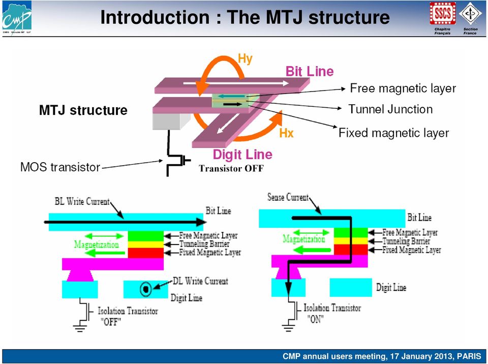
2 Introduction : The MTJ structure
3 CMOS - MTJ Process CMOS process done at the foundry (stop at the top metal layer) CMOS
")
4 CMOS - MTJ Process CMOS process done at the foundry (stop at the top metal layer) Magnetic post-process + metallization + passivation + pad openings Magnetic CMOS


5 MTJ above-ic on CMOS process CILOMAG Consortium Silicon Foundries MTJ Postprocess 0.35µ STMicroelectronics 130nm


 Packaging Démonstrateur 2 Filière JTM Système de calcul basse consommation")
6 11 partners Spintronics Platform for Innovative Nanotechnology Démonstrateur 1 Filière Spin-valve Capteurs pour la la Santé et et l électronique de puissance Technologie BE >250nm Spintronics Platform for Innovative Nanotechnologies Conception / design ( Plateforme Saclay) Layout/ assemblage / gestion MPW FE CMOS BE magnétique ( Plateforme Grenoble) Packaging Démonstrateur 2 Filière JTM Système de calcul basse consommation Technologie BE 120nm
 Packaging Démonstrateur 2 Filière JTM Système de calcul basse consommation")
7 Spintronics Platform for Innovative Nanotechnology LIRMM SPEC LIST LETI-DCIS MENTA Design Sensor / Logic + ASIC design for Sensors SPINTEC IEF CMP CROCUS Magnetic Process Design Kit Digital PDK+ PDK for sensors LETI/DIHS LTM Ligne BE magnétique + Dépôt 200mm IBS AVIZA + Carac magnéto-transport CAPRES + Four de recuit 200mm + Gravure RIE pour Spintronique

8 CMOS-MTJ First Prototype Designer : LIRMM (Montpellier) Application : Non Volatile FPGA test structures prototype. CMOS process : Austriamicrosystems 0.35um CMOS CMP MPW run : A35C7-2 Magnetic Post-Process : INESC (Portugal) First CMOS / MTJ Prototype in a MPW run

9 CMOS-MTJ Second Prototype Designers : All CILOMAG partners Application : Different blocks architectures. CMOS process : Austriamicrosystems 0.35um CMOS CMP MPW run : A35C8-2 Magnetic Post-Process : LIMN / LETI (Grenoble) Embedded MTJ/CMOS sub-mpw run

10 CMOS-MTJ 3rd Prototype Designers : All SPIN partners Application : CMOS/Magnetic blocks and test structures. CMOS process : STMicroelectronics 130nm CMOS CMP MPW run : S13C09-4 Magnetic Post-Process : LIMN / LETI (Grenoble)

11 CMOS-MTJ 4th Prototype Designers : SPIN partners LIRMM Application : CMOS/Magnetic FPGA. (25mm 2 ) CMOS process : STMicroelectronics 130nm CMOS CMP MPW run : S13C10-3 Magnetic Post-Process : LIMN / LETI (Grenoble)

12 CMOS-MTJ 5th Prototype Designers : All SPIN partners Application : CMOS/Magnetic blocks and test structures. CMOS process : STMicroelectronics 130nm CMOS CMP MPW run : S13C10-3 Magnetic Post-Process : LIMN / LETI (Grenoble)


13 ANR / P2N DIPMEM Project Project just starting addressing : Hybrid Magnetic/CMOS design and manufacturing Resistive RAM like circuitry for non-volatile logics. ANR / P2N DIPMEM

14 Perspectives Complete Hybrid CMOS/Magnetic design-kits. DIPMEM project target 28nm CMOS. External users may interact with the consortium to have the access.

MEMS Processes from CMP
 MEMS Processes from CMP MUMPS from MEMSCAP Bulk Micromachining 1 / 19 MEMSCAP MUMPS processes PolyMUMPS SOIMUMPS MetalMUMPS 2 / 19 MEMSCAP Standard Processes PolyMUMPs 8 lithography levels, 7 physical
AMAGNETIC TUNNEL JUNCTION (MTJ) is a vertical
 is a vertical") IEEE TRANSACTIONS ON MAGNETICS, VOL. 47, NO. 11, NOVEMBER 2011 4611 A High-Reliability, Low-Power Magnetic Full Adder Yi Gang 1;2, Weisheng Zhao 1;2, Jacques-Olivier Klein 1;2, Claude Chappert 1;2, and
IEEE TRANSACTIONS ON MAGNETICS, VOL. 47, NO. 11, NOVEMBER 2011 4611 A High-Reliability, Low-Power Magnetic Full Adder Yi Gang 1;2, Weisheng Zhao 1;2, Jacques-Olivier Klein 1;2, Claude Chappert 1;2, and
State-of-Art (SoA) System-on-Chip (SoC) Design HPC SoC Workshop
 System-on-Chip (SoC) Design HPC SoC Workshop") Photos placed in horizontal position with even amount of white space between photos and header State-of-Art (SoA) System-on-Chip (SoC) Design HPC SoC Workshop Michael Holmes Manager, Mixed Signal ASIC/SoC
Photos placed in horizontal position with even amount of white space between photos and header State-of-Art (SoA) System-on-Chip (SoC) Design HPC SoC Workshop Michael Holmes Manager, Mixed Signal ASIC/SoC
From physics to products
 From physics to products From MRAM to MLU and beyond memory Magnetic Random Access Memory Magnetic Logic Unit Lucien Lombard Crocus-Technology Overview 1 - The semiconductor industry 2 - Crocus-Technology
Concevoir et produire des semiconducteurs en Europe: une Utopie? Let s have a look
 Concevoir et produire des semiconducteurs en Europe: une Utopie? Let s have a look Gérard MATHERON MIDIS MINATEC 24 avril 2009 1 Advanced Wafer Manufacturing Challenges Advanced Wafer Manufacturing Challenges
Design-Kits, Libraries & IPs
 Design-Kits, Libraries & IPs Supported CAD tools Design-kits overview Digital, Analog, and RF Libraries IPs Supported CAD tools Design-kits overview ST 65nm Tanner PDK Standard cell Libraries IPs austriamicrosystems
1. Submission Rules. 2. Verification tools. 3. Frequent errors
 Design Submission 1. Submission Rules 2. Verification tools 3. Frequent errors Design submission rules 1. Send the submission form in the same time as the circuit database 2. The GDSII file must have a.gds
Soitec. Eric Guiot, Manager R&D Soitec. 7 mars 2011 JSIam 2011
 Soitec Eric Guiot, Manager R&D Soitec 1 Agenda Soitec: company presentation Applications and market PhDs at Soitec 2 Mission Statement Supply innovative materials and technologies for the electronics and
On the convergences between More Moore, More Than Moore and Beyond CMOS
 On the convergences between More Moore, More Than Moore and Beyond CMOS Workshop organizers : Francis BALESTRA & Raphael CLERC IMEP, Grenoble, FRANCE Thank you to A. Godoy and colleagues for the help organizing
How To Integrate 3D-Ic With A Multi Layer 3D Chip
 3D-IC Integration Developments Cooperation for servicing and MPW runs offering Agenda Introduction Process overview Partnership for MPW runs service 3D-IC Design Platform First MPW run Conclusion 3D-IC
3D-IC Integration Developments & Cooperations for servicing
 Ecole de microélectronique et microsystèmes 16-19 mai 2011, Fréjus 3D-IC Integration Developments & Cooperations for servicing Kholdoun TORKI [email protected] CMP 46, Avenue Félix Viallet, 38031
Agenda. Michele Taliercio, Il circuito Integrato, Novembre 2001
 Agenda Introduzione Il mercato Dal circuito integrato al System on a Chip (SoC) La progettazione di un SoC La tecnologia Una fabbrica di circuiti integrati 28 How to handle complexity G The engineering
STMicroelectronics. Deep Sub-Micron Processes 130nm, 65 nm, 40nm, 28nm CMOS, 28nm FDSOI. SOI Processes 130nm, 65nm. SiGe 130nm
 STMicroelectronics Deep Sub-Micron Processes 130nm, 65 nm, 40nm, 28nm CMOS, 28nm FDSOI SOI Processes 130nm, 65nm SiGe 130nm CMP Process Portfolio from ST Moore s Law 130nm CMOS : HCMOS9GP More than Moore
Emerging storage and HPC technologies to accelerate big data analytics Jerome Gaysse JG Consulting
 Emerging storage and HPC technologies to accelerate big data analytics Jerome Gaysse JG Consulting Introduction Big Data Analytics needs: Low latency data access Fast computing Power efficiency Latest
Welcome & Introduction
 Welcome & Introduction Accelerating the next technology revolution Sitaram Arkalgud, PhD Director Interconnect Temporary Bond Workshop SEMICON West July 11, 2011 San Francisco CA Copyright 2008 SEMATECH,
3D innovations: From design to reliable systems
 3D innovations: From design to reliable systems Uwe Knöchel, Andy Heinig Fraunhofer IIS, Design Automation Division Zeunerstraße 38, 01069 Dresden [email protected] Phone: +49 351 4640
System-on. on-chip Design Flow. Prof. Jouni Tomberg Tampere University of Technology Institute of Digital and Computer Systems. jouni.tomberg@tut.
 System-on on-chip Design Flow Prof. Jouni Tomberg Tampere University of Technology Institute of Digital and Computer Systems [email protected] 26.03.2003 Jouni Tomberg / TUT 1 SoC - How and with whom?
MARKET ANALYSIS AND KEY TRENDS FROM FD SOI PERSPECTIVE (SEPTEMBER 22, 2014)
") MARKET ANALYSIS AND KEY TRENDS FROM FD SOI PERSPECTIVE (SEPTEMBER 22, 2014) INTERNATIONAL BUSINESS STRATEGIES, INC. 632 Industrial Way Los Gatos CA 95030 USA 408 395 9585 408 395 5389 (fax) www.ibs-inc.net
MARKET ANALYSIS AND KEY TRENDS FROM FD SOI PERSPECTIVE (SEPTEMBER 22, 2014) INTERNATIONAL BUSINESS STRATEGIES, INC. 632 Industrial Way Los Gatos CA 95030 USA 408 395 9585 408 395 5389 (fax) www.ibs-inc.net
Nanotechnologies for the Integrated Circuits
 Nanotechnologies for the Integrated Circuits September 23, 2015 Dr. Bertrand Cambou Professor of Practice NAU, Cybersecurity School of Informatics, Computing, and Cyber-Systems Agenda The Market Silicon
CMS Tracker module / hybrid tests and DAQ development for the HL-LHC
 CMS Tracker module / hybrid tests and DAQ development for the HL-LHC S. Mersi, G. Auzinger [email protected] 1 Outline Reminder: the Ph2 CMS Tracker upgrade pt Modules: principle, elements, electronics
Complete ASIC & COT Solutions 1986-2008
 Complete ASIC & COT Solutions 1986-2008 www.avnet-asic.com Nadav Ben-Ezer Managing Director 1 March 5th, 2008 Core Business ASIC/SoC Design and Implementation RTL Design Sub-system IP Integration RTL to
SANOFI. A diversified global healthcare leader, focused on patients needs. By Mohammed Charki Massy Sept 20th
 SANOFI A diversified global healthcare leader, focused on patients needs Sanofi Profile Welcome you at Massy www.sanofi.com Tertiary site Beggining 2010 : a brand new site has been built on the old Clin
Creating Affordable Silicon
 Creating Affordable Silicon John Tinson VP Sales Sondrel 2016 03/05/2016 Presentation Title 1 The IoT Challenge Existing OEM s and start ups would benefit from a custom ASIC to prove their application
Pre-tested System-on-Chip Design. Accelerates PLD Development
 Pre-tested System-on-Chip Design Accelerates PLD Development March 2010 Lattice Semiconductor 5555 Northeast Moore Ct. Hillsboro, Oregon 97124 USA Telephone: (503) 268-8000 www.latticesemi.com 1 Pre-tested
Silicon Cluster Grenoble Microelectronics ICT and beyond
 Silicon Cluster Grenoble Microelectronics ICT and beyond Dominique THOMAS STMicroelectronics V. Pequignat E Semet I. Guillaume The Grenoble «Silicon Valleys» 2 Microelectronics in Grenoble Microsystems
VON BRAUN LABS. Issue #1 WE PROVIDE COMPLETE SOLUTIONS ULTRA LOW POWER STATE MACHINE SOLUTIONS VON BRAUN LABS. State Machine Technology
 VON BRAUN LABS WE PROVIDE COMPLETE SOLUTIONS WWW.VONBRAUNLABS.COM Issue #1 VON BRAUN LABS WE PROVIDE COMPLETE SOLUTIONS ULTRA LOW POWER STATE MACHINE SOLUTIONS State Machine Technology IoT Solutions Learn
Procedure to get a design kit
 Design kits Procedure to get a design kit Design kits available at CMP Design kits distribution Procedure to handle DK requests Customer request : http://cmp.imag.fr Design kit request form http://cmp.imag.fr/
NVM memory: A Critical Design Consideration for IoT Applications
 NVM memory: A Critical Design Consideration for IoT Applications Jim Lipman Sidense Corp. Introduction The Internet of Things (IoT), sometimes called the Internet of Everything (IoE), refers to an evolving
Evaluating AC Current Sensor Options for Power Delivery Systems
 Evaluating AC Current Sensor Options for Power Delivery Systems State-of-the-art isolated ac current sensors based on CMOS technology can increase efficiency, performance and reliability compared to legacy
IBS - Ion Beam Services
 IBS - Ion Beam Services Profile Technologies Devices & sensor fabricat ion Participation to R&D programs Researched partnership Présentation activité composant 1 Profile : Products and services Product
Build your own solution with UMS
 FOUNDRY SERVICES Build your own solution with UMS Your innovative partner for high performance, high yield MMIC solutions 2015-2016 www.ums-gaas.com FOUNDRY SERVICES UMS has developed a proven family of
Primauté industrielle. Photonique dans LEIT TIC
 Primauté industrielle Photonique dans LEIT TIC ICT in Industrial Leadership (LEIT) Excellent science ICT in Industrial leadership Societal challenges 2 Industrial Leadership - ICT P A new generation of
Dual Integration - Verschmelzung von Wafer und Panel Level Technologien
 ERÖFFNUNG DES INNOVATIONSZENTRUMS ADAPTSYS Dual Integration - Verschmelzung von Wafer und Panel Level Technologien Dr. Michael Töpper BDT Introduction Introduction Why do we need such large machines to
Leti Introduction and Overview
 Leti Introduction and Overview Leti Day in Tokyo, October 3rd 2012 Laurent Malier 2012 Leti 2012 1 CEA The CEA at a glance Commissariat à l Énergie Atomique et aux Énergies Alternatives is one of the largest
From Technologies to Applications
 Laboratoire d électronique et de technologie de l information From Technologies to Applications J.R. Lèquepeys, Head of Silicon Component Division 2012 INTEL ERIC - 2012 1 AGENDA Brief overview of CEA-Leti
Interactive Interface USERS /CMP
 Web site: http://cmp.imag.fr General informations Specific informations and forms Interface Users / CMP General informations Web site: Home page Quick References News Upcoming RUNS Customers login General
Designing a System-on-Chip (SoC) with an ARM Cortex -M Processor
 with an ARM Cortex -M Processor") Designing a System-on-Chip (SoC) with an ARM Cortex -M Processor A Starter Guide Joseph Yiu November 2014 version 1.02 27 Nov 2014 1 - Background Since the ARM Cortex -M0 Processor was released a few years
Designing a System-on-Chip (SoC) with an ARM Cortex -M Processor A Starter Guide Joseph Yiu November 2014 version 1.02 27 Nov 2014 1 - Background Since the ARM Cortex -M0 Processor was released a few years
Bits of the Future : Impact of GMR on magnetic information storage
 Bits of the Future : Impact of GMR on magnetic information storage History of magnetic recording Introduction to reading data Basics of GMR sensors Next generation heads TMR, CPP-GMR Challenges/outlooks
Electronics Technology
 Teacher Assessment Blueprint Electronics Technology Test Code: 5907 / Version: 01 Copyright 2011 NOCTI. All Rights Reserved. General Assessment Information Blueprint Contents General Assessment Information
Reconfigurable System-on-Chip Design
 Reconfigurable System-on-Chip Design MITCHELL MYJAK Senior Research Engineer Pacific Northwest National Laboratory PNNL-SA-93202 31 January 2013 1 About Me Biography BSEE, University of Portland, 2002
New Ferroelectric Material for Embedded FRAM LSIs
 New Ferroelectric Material for Embedded FRAM LSIs V Kenji Maruyama V Masao Kondo V Sushil K. Singh V Hiroshi Ishiwara (Manuscript received April 5, 2007) The strong growth of information network infrastructures
2014 EMERGING NON- VOLATILE MEMORY & STORAGE TECHNOLOGIES AND MANUFACTURING REPORT
 2014 EMERGING NON- VOLATILE MEMORY & STORAGE TECHNOLOGIES AND MANUFACTURING REPORT COUGHLIN ASSOCIATES SAN JOSE, CALIFORNIA April 2014 2014 Emerging NV Memory & Storage Technologies and Manufacturing Report
Figure 1. New Wafer Size Ramp Up as a Percentage of World Wide Silicon Area Versus Years Elapsed Since the New Size Was Introduced [1].
![Figure 1. New Wafer Size Ramp Up as a Percentage of World Wide Silicon Area Versus Years Elapsed Since the New Size Was Introduced [1].](/thumbs/23/1973496.jpg "Figure 1. New Wafer Size Ramp Up as a Percentage of World Wide Silicon Area Versus Years Elapsed Since the New Size Was Introduced [1].") White Paper Forecasting the 45mm Ramp Up IC Knowledge LLC, PO Box 2, Georgetown, MA 1833 Tx: (978) 352 761, Fx: (978) 352 387, email: [email protected] Introduction The introduction and ramp up of 45mm
White Paper Forecasting the 45mm Ramp Up IC Knowledge LLC, PO Box 2, Georgetown, MA 1833 Tx: (978) 352 761, Fx: (978) 352 387, email: [email protected] Introduction The introduction and ramp up of 45mm
Coherent sub-thz transmission systems in Silicon technologies: design challenges for frequency synthesis
 Coherent sub-thz transmission systems in Silicon technologies: design challenges for frequency synthesis Alexandre Siligaris www.cea.fr Cliquez pour modifier le style du Outline titre Introduction-context
FLASH TECHNOLOGY DRAM/EPROM. Flash. 1980 1982 1984 1986 1988 1990 1992 1994 1996 Year Source: Intel/ICE, "Memory 1996"
 10 FLASH TECHNOLOGY Overview Flash memory technology is a mix of EPROM and EEPROM technologies. The term flash was chosen because a large chunk of memory could be erased at one time. The name, therefore,
Hitachi Europe R&D. Dr. David Williams. Activity in Europe. Hitachi Cambridge Laboratory. March 2014
 Hitachi Europe R&D (ERD) Activity in Europe March 2014 Dr. David Williams Hitachi Cambridge Laboratory Contents 1. General information 2. ICT and Big Data Laboratories 3. Cambridge Laboratory 1 1-1 Hitachi
Séries U3-CMOS. Nouvelles. Caméras Numériques USB3. Ultra rapides
 Séries U3-CMOS Nouvelles Caméras Numériques USB3 Ultra rapides 1 Cette nouvelle série de caméras pour la microscopie et adaptée à un grand nombre d applications. 2 Fabrications et contrôles en salles blanches
Miniaturizing Flexible Circuits for use in Medical Electronics. Nate Kreutter 3M
 Miniaturizing Flexible Circuits for use in Medical Electronics Nate Kreutter 3M Drivers for Medical Miniaturization Market Drivers for Increased use of Medical Electronics Aging Population Early Detection
NATIONAL SUN YAT-SEN UNIVERSITY
 NATIONAL SUN YAT-SEN UNIVERSITY Department of Electrical Engineering (Master s Degree, Doctoral Program Course, International Master's Program in Electric Power Engineering) Course Structure Course Structures
European bespoke wafer processing & development solutions for : Grinding, CMP, Edge Treatment, Wafer Bonding, Dicing and Cleaning
 European bespoke wafer processing & development solutions for : Grinding, CMP, Edge Treatment, Wafer Bonding, Dicing and Cleaning Georges Peyre : Sales & Marketing Director SEMICON Europa Grenoble - 2014
Code generation under Control
 Code generation under Control Rencontres sur la compilation / Saint Hippolyte Henri-Pierre Charles CEA Laboratoire LaSTRE / Grenoble 12 décembre 2011 Introduction Présentation Henri-Pierre Charles, two
Status of CBM-XYTER Development
 Status of CBM-XYTER Development Latest Results of the CSA/ADC Test-Chip Tim Armbruster [email protected] Heidelberg University Schaltungstechnik Schaltungstechnik und und 14th CBM CM
Security testing for hardware product : the security evaluations practice
 Alain MERLE CESTI LETI CEA Grenoble [email protected] Security testing for hardware product : the security evaluations practice DCIS/SASTI/CESTI 1 Abstract «What are you doing in ITSEFs?» Testing, Security
ECE 410: VLSI Design Course Introduction
 ECE 410: VLSI Design Course Introduction Professor Andrew Mason Michigan State University Spring 2008 ECE 410, Prof. A. Mason Lecture Notes Page i.1 Age of electronics microcontrollers, DSPs, and other
Web and Big Data at LIG. Marie-Christine Rousset (Pr UJF, déléguée scientifique du LIG)
") Web and Big Data at LIG Marie-Christine Rousset (Pr UJF, déléguée scientifique du LIG) Data and Knowledge Processing at Large Scale Officers: Massih-Reza Amini - Jean-Pierre Chevallet Teams: AMA EXMO GETALP
Web and Big Data at LIG Marie-Christine Rousset (Pr UJF, déléguée scientifique du LIG) Data and Knowledge Processing at Large Scale Officers: Massih-Reza Amini - Jean-Pierre Chevallet Teams: AMA EXMO GETALP
Track Trigger and Modules For the HLT
 CMS L1 Track Trigger for SLHC Anders Ryd for the CMS Track Trigger Task Force Vertex 2009 Sept. 13-18, 2009 L=1035 cm-2s-1 Outline: SLHC trigger challenge Tracking triggers Track trigger modules Simulation
Hardware and software implications of creating Bluetooth Scatternet devices
 Hardware and software implications of creating Bluetooth Scatternet devices David Johnson Abstract This paper seeks to explain the practical issues encountered when implementing point to multipoint capable
Processi chimici localizzati per il fotovoltaico
 Processi chimici localizzati per il fotovoltaico M. Balucani Rise Technology S.r.l. Lung. P. Toscanelli 170 00121 Roma ENEA: Stato e prospettive del fotovoltaico in Italia June 26, 2014 Who is Rise Technology
Here are my slides from lecture, along with my notes about each slide.
 Chapter 3: Storage Here are my slides from lecture, along with my notes about each slide. NOTE: You are expected to attend all class meetings. Please be in the room when class begins and be ready to participate
UTBB-FDSOI 28nm : RF Ultra Low Power technology for IoT
 UTBB-FDSOI 28nm : RF Ultra Low Power technology for IoT International Forum on FDSOI IC Design B. Martineau www.cea.fr Cliquez pour modifier le style du Outline titre Introduction UTBB-FDSOI 28nm for RF
FRT - setting the standard
 FRT - setting the standard Surface Analysis Metrology Instruments Process Control Chromatic white light sensor Weißlicht Specs: Linse blauer Fokus roter Fokus max height range 300 µm 600 µm 3 mm 10 mm
Grid e-services for Multi-Layer SOM Neural Network Simulation
 Grid e-services for Multi-Layer SOM Neural Network Simulation,, Rui Silva Faculdade de Engenharia 4760-108 V. N. Famalicão, Portugal {rml,rsilva}@fam.ulusiada.pt 2007 Outline Overview Multi-Layer SOM Background
Implementation Of High-k/Metal Gates In High-Volume Manufacturing
 White Paper Implementation Of High-k/Metal Gates In High-Volume Manufacturing INTRODUCTION There have been significant breakthroughs in IC technology in the past decade. The upper interconnect layers of
SiP & Embedded Passives ADEPT-SiP Project
 System-in-Package () and the ADEPT- Project David Pedder TWI Ltd, Granta Park, Great Abington, Cambridge Copyright 2006 ADEPT- & Embedded Passives ADEPT- Project Objectives Programme Partners ADEPT- Architecture
3D Printing: Systems, Materials, Tips & Tricks for Research Prototypes and Beyond. Lessons from the Velo Gripper project
 3D Printing: Systems, Materials, Tips & Tricks for Research Prototypes and Beyond Lessons from the Velo Gripper project Contributors The team: Matei Ciocarlie Bob Holmberg Scott Stanford Mike Schlicht
LASP Electrical Engineer Group Capabilities
 LASP Electrical Engineer Group Capabilities Neil White Phone: 303-492-7959 Email: [email protected] The 29 th annual National Space Symposium April 8-12 Planetary Science Space Physics Solar
Semi Networking Day Packaging Key for System Integration
 Semi Networking Day Packaging Key for System Integration Le Quartz, 75 Cours Emile Zola 69100 Villeurbanne, France Tel : +33 472 83 01 80 - Fax : +33 472 83 01 83 Web: http://www.yole.fr Semi Networking
Research Report: The Arista 7124FX Switch as a High Performance Trade Execution Platform
 Research Report: The Arista 7124FX Switch as a High Performance Trade Execution Platform Abstract: Many groups are working on reducing trading execution latency - the time from a critical Ethernet frame
NAND Flash FAQ. Eureka Technology. apn5_87. NAND Flash FAQ
 What is NAND Flash? What is the major difference between NAND Flash and other Memory? Structural differences between NAND Flash and NOR Flash What does NAND Flash controller do? How to send command to
NXP PN548 (65V10) Near Field Communication Module
 Near Field Communication Module") NXP PN548 (65V10) Module Basic Functional Analysis 1891 Robertson Road, Suite 500, Ottawa, ON K2H 5B7 Canada Tel: 613-829-0414 chipworks.com Basic Functional Analysis 2 Some of the information in this
NXP PN548 (65V10) Module Basic Functional Analysis 1891 Robertson Road, Suite 500, Ottawa, ON K2H 5B7 Canada Tel: 613-829-0414 chipworks.com Basic Functional Analysis 2 Some of the information in this
DEVELOPMENTS & TRENDS IN FEOL MATERIALS FOR ADVANCED SEMICONDUCTOR DEVICES Michael Corbett [email protected] Semicon Taiwan2015
 DEVELOPMENTS & TRENDS IN FEOL MATERIALS FOR ADVANCED SEMICONDUCTOR DEVICES Michael Corbett [email protected] Semicon Taiwan2015 LINX BACKGROUND Linx Consulting 1. We help our clients to succeed
Advanced VLSI Design CMOS Processing Technology
 Isolation of transistors, i.e., their source and drains, from other transistors is needed to reduce electrical interactions between them. For technologies
White Paper 40-nm FPGAs and the Defense Electronic Design Organization
 White Paper 40-nm FPGAs and the Defense Electronic Design Organization Introduction With Altera s introduction of 40-nm FPGAs, the design domains of military electronics that can be addressed with programmable
Heterogeneous Technology Alliance
 Heterogeneous Technology Alliance Represented by André Perret CEO The partners CSEM, Inc. company, 400 empl. Micro & nanotechnologies, systems engineering, information and communication technologies, photonics,
Titre: Required Information For Submitting Databases to TELEDYNE DALSA Design & Product Support.
 Titre: Required Information For Submitting Databases to TELEDYNE DALSA Design & Product Support. Document : DES-0002.11 Création du document : December 22th, 2004 Bromont, Québec, Canada 2 DE 7 Database
On a New Way to Read Data from Memory
 On a New Way to Read Data from Memory David Samyde 1, Sergei Skorobogatov 2, Ross Anderson 2 and Jean-Jacques Quisquater 1 1: Université catholique de Louvain, UCL Crypto Group Place du Levant, 3, B-1348
FPGA Prototyping Primer
 FPGA Prototyping Primer S2C Inc. 1735 Technology Drive, Suite 620 San Jose, CA 95110, USA Tel: +1 408 213 8818 Fax: +1 408 213 8821 www.s2cinc.com What is FPGA prototyping? FPGA prototyping is the methodology
Smart Card Security How Can We Be So Sure?
 Smart Card Security How Can We Be So Sure? Ernst Bovelander TNO Centre for Evaluation of Instrumentation and Security Techniques PO Box 5013 2600 GA Delft, The Netherlands [email protected] 1. Introduction
On Security Evaluation Testing
 On Security Evaluation Testing Kerstin Lemke-Rust Hochschule Bonn-Rhein-Sieg Workshop: Provable Security against Physical Attacks Lorentz Center, 19 Feb 2010 Kerstin Lemke-Rust (H BRS) On Security Evaluation
Silicon Seminar. Optolinks and Off Detector Electronics in ATLAS Pixel Detector
 Silicon Seminar Optolinks and Off Detector Electronics in ATLAS Pixel Detector Overview Requirements The architecture of the optical links for the ATLAS pixel detector ROD BOC Optoboard Requirements of
Fall 2009. Lecture 1. Operating Systems: Configuration & Use CIS345. Introduction to Operating Systems. Mostafa Z. Ali. [email protected].
 Fall 2009 Lecture 1 Operating Systems: Configuration & Use CIS345 Introduction to Operating Systems Mostafa Z. Ali [email protected] 1-1 Chapter 1 Introduction to Operating Systems An Overview of Microcomputers
Silicon Photonics Market & Applications
 Silicon Photonics Market & Applications 2013 Fields of Expertise Yole Developpement is a market, technology and strategy consulting company, founded in 1998. We operate in the following areas: Power Electronics
SPADIC: CBM TRD Readout ASIC
 SPADIC: CBM TRD Readout ASIC Tim Armbruster [email protected] HIC for FAIR, Darmstadt Schaltungstechnik Schaltungstechnik und und February 2011 Visit http://spadic.uni-hd.de 1. Introduction
INF4420. Outline. Layout and CMOS processing technology. CMOS Fabrication overview. Design rules. Layout of passive and active componets.
 INF4420 Layout and CMOS processing technology Spring 2012 1 / 76 Outline CMOS Fabrication overview Design rules Layout of passive and active componets Packaging 2 / 76 Introduction As circuit designers
Benefits of a Colter OEM design / Embeded PLC
 Introduction have the capability to design special OEM modules or embedded PLCs to suit your exact needs based on our standard FMT-100 and FMT-200 range. The modular construction of these products makes
WWW.CABLEJOINTS.CO.UK THORNE & DERRICK UK TEL 0044 191 490 1547 FAX 0044 477 5371 TEL 0044 117 977 4647 FAX 0044 977 5582 WWW.THORNEANDDERRICK.CO.
 able leats Section 6 able leats for Power Transmission ables Glass reinforced composite cable cleats general information type able cleat U type able cleat (channel mounted) T type able cleat (trefoil configuration)
The pole Optique-Rhône. Rhône-Alpes: a booster of innovation in Optics&Photonics
 The pole Optique-Rhône Rhône-Alpes: a booster of innovation in Optics&Photonics The scientific and industrial forces of Rhône-Alpes region 1 000 20 000 5 400 8 000 1 000 1 000 2 500 1 500 500 2 500 1 500