Simon McElrea : BiTS
|
|
|
- Michael May
- 10 years ago
- Views:
Transcription

1 Interconnectology The Road to 3D Mobile Consumer Driven Market This Changes Everything 1 Simon McElrea : BiTS

2 What Is Advanced/3D Packaging? 2 This Is... But So Is This. The level of Hardware Engineering now required to build the miniaturized & wearable devices of tomorrow, is Package Engineering (what Invensas calls Interconnectology).

 32% 50% 40% 30% 20% Flip Wafer Chip Level DCA Flip Chip Package 14% 20% 10% 0% 3D TSV 1990 1995 2000 2005 2010 2015 2020 $6Bn 10% CAAGR")
3 Percent of IC Package Value Add The Packaging Pizza Pie Chart ( ) 100% 90% Wire Bond (Leadframe/Module) 80% IC PACKAGE VALUE TREND Kc bp package value 19% 70% 60% Wire Bond (BGA/CSP) 32% 50% 40% 30% 20% Flip Wafer Chip Level DCA Flip Chip Package 14% 20% 10% 0% 3D TSV $6Bn 10% CAAGR $25Bn 6% CAAGR $59Bn 15% 3 PRISMARK, PIZZA HUT

4 The Value Is In The Flavor, Not The Size of The Slice UTILIZED DIE AREA BY PACKAGE TYPE 2011 Flip Chip 12% Flip Chip 16% DCA/ Wafer CSP 2% FC BGA/ LGA/CSP COF/COG 5% COB 3% DCA/ COF/COG Wafer CSP 4% 4.5% 2016 Leadframe 5% 24% FC BGA/ Leadframe LGA/CSP 22% 8% COB 2% CAAGR % Stacked CSP 24% BOC CSP 17% Wire Bond BGA/CSP 7% Discrete/LED 13% Stacked CSP 26% Kc bp-package3 BOC CSP 14% Discrete/LED 14% Wire Bond BGA/CSP 6% Total: 6.1M m 2 Total: 9.0M m 2 Although the die area per package technology (line loading) is hardly changing, the return on the advanced nodes, flip-chip, stacked-csp, WLP, is growing at 20% CAGR. 4 PRISMARK


5 As The Pie Grows, New Slices Get Added FOUNDRY MIDDLE END OSAT BGA/ CSP FEOL BEOL PKG. ASSY FT 1990s FLIP- CHIP FEOL BEOL RDL Wafer Bumping WL Test PKG. ASSY FT 2000s 3DIC FEOL Via Middle BEOL Micro- Bumping Thin & Reveal Interposer TSV Fab WL-Carrier Assembly 3D WL-Test 2.5D ASSY PKG. ASSY FT 2010s Invensas Focus 2016 $400b+ ~$10b (Largest Growth Segment) $40b+ 5


6 The Middle End Ingredients m 6

7 Long Term Advanced Packaging Roadmap This Makes OSAT Roadmaps Look Like RF Baseband Processor Sensor PMIC 2.5D TSV 20nm Partitioning Cu Pillar C-o-C Memory Cube Package Stacking C-o-C 2.5D GPU + HBM TSV Embedded Die 2.5D TSV 14nm Partitioning APU SoC Deconstruct 3D TSV Heterogeneous Die Stacking Si Photonics Market: Market: Market: Market: Market: FPGA Mobile Network Processors Network Tablet Processors Network Mobile, Tablet Processors Network Mobile, Tablet Time This is a remarkable change from when I was at Amkor (2000- For Controlled Release at the IPC Component Technology Conference 2006). AMKOR 47 Sep-13, R.Huemoeller

8 And It Makes Supply Chain Roadmaps Look Like 1 2 YIKES! Yikes! 8 YOLE

9 And That s The Key MIDDLE END RDL Wafer Bumping WL Test Micro- Bumping Thin & Reveal Interposer TSV Fab WL-Carrier Assembly 2.5D ASSY The adoption curve depends on which players the supply chain (market) permits to own the new value-added elements. History says: it s the model that provides the greatest sourcing flexibility to the end product owners. 9

10 What Are The 3D Drivers? Mobile Consumer Driven Market This Changes Everything 10


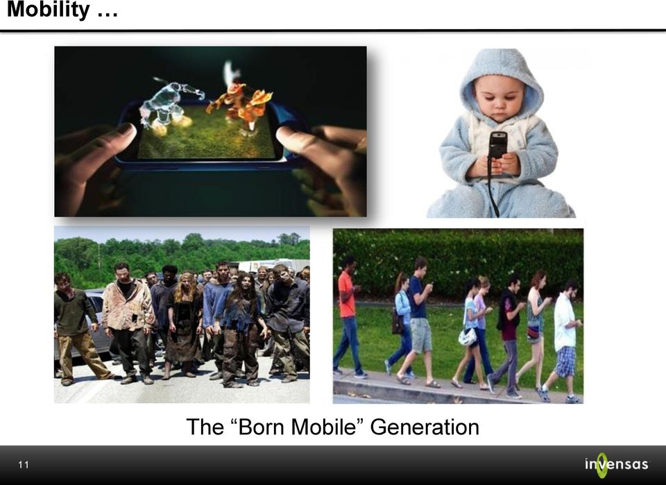
11 Mobility The Born Mobile Generation 11
12 and The Internet of Every Thing 12 IDC

13 How Many Things? 10 7 Internet infrastructure servers, networking Cars; appliances PCs; smartphones; tablets; watches; TVs; people; clocks; radios Headsets; peripherals; lights and switches; anything with a battery Tags, tickets Pills 13 GARTNER


14 Yes, Its Exponential My Dear Watson 14 DR. MORRIS CHANG


15 Speaking of Watson By the end of this decade, the equivalent of Watson will fit in our pocket. Dr. John Kelly 15 IBM

16 The New Normal: Lower Semiconductor Content/System 16 GARTNER


17 Front End vs. Back End Growth FOUNDRY BACK END ~5% ~15% 17 GARTNER


18 Your Back End Is Bigger Than You Think And Your Middle End is Huge 18

19 The Killer App That Created Advanced Packaging? Mobile Consumer Driven Market This Changes Everything 19

20 The Mobile Phone, Of Course... The Mobile Phone Drove The Creation of the Stacked-Chip CSP Package, System-in-Package, Package-on-Package, the Wafer- Level & Fan-Out Wafer Level Package, along with a host of CMOS Image & Touch Sensor Packages, MEMS Sensor Packages, and 2.5/3DIC Solutions. 20

21 Advanced 3D Packaging Now Dominates The BOM Macronix: Serial Flash CSP Elpida:LPDDR2 Stacked-CSP Apple: ACPU PoP BRCM: Touchs CSP QCOM: TRX+GPS CSP QCOM: BB Stacked-CSP TI: Touchscreen CSP ST: MEMS Acc. Back SWKS: Quad Band PA SiP SWKS: W- CDMA PA SiP QCOM: Power CSP TQNT: Switch SiP SanDisk: NAND Stacked-CSP Apple/Cirrus: Audio CSP ST: MEMS Acc. TQNT: W- CDMA PA SiP SWKS: LTE PA SiP Apple/Cirrus: Audio CSP Apple: Power Mgmt. CSP BCOM: Wifi Bluetooth SiP 21 APPLE iphone 5s
 accounts for over")
22 BOM Breakdown (By $) D Packaging (Package on Package & Stacked Die CSP) accounts for over 2/3 of the packaged-ic BOM cost (~$80). 22 TECHINSIGHTS
23 Why The PoP Love Affair? 23
24 Bandwidth (GB/s) Hence The Never-Ending Need For Advanced PoP Wide-IO 3DIC I/O Wide I/O BVA PoP 12.8 Cu-Pillar PoP BGA/TMV PoP PoP: I/O mm Pitch PoP: <400I/O mm Pitch
25 But Why 3DIC? Mobile Consumer Driven Market This Changes Everything 25

26 Why 3D?: It s Mostly About Cost Advanced Silicon Nodes Driving Higher Costs Moore s Law is a Law of Economics. 26


27 But It s Also About Cost Cost of Scaling The cost per fab, R&D cost per node, and design cost per device, grow beyond a tipping point below 20nm. 3DIC design architecture allows technologies to be built at the right node and then stacked, which is much more cost-effective overall, and not exclusive to 2-3 players. 27
28 Its Also About Power Power Efficiency CMOS + TSV Wide IO + TSV stack CMOS + Interposer DDR3 + Interposer 9.64 Hynix 16 Gb LPDDR3 + POP Micron2Gb LPDDR2 + POP 2Gb DDR 3 + DIMM CPU 91 mm DIMM (mw/gbps) Orders Of Magnitude Power Savings (Mobile Battery Life or Data Center Cost) Are Possible in 3DIC 28


29 So Are We There Yet? By ITRS definition, We Are There! Between the FPGA, Memory Cube, Wide-IO and Interposer-based products we are at this inflection point! 29 ITRS

30 30

31 So We Said The Supply Chain Was The Key Indicator INFLECTION 31 GARTNER
32 3DIC Equipment LEADING Suppliers POTENTIAL Surveyed SUPPLIERS OF TSV RELATED PROCESS EQUIPMENT Process Step Wafer Thinning/Stress Reduction Via Patterning (Lithography/Stepper) Via Etch (DRIE/Bosch) Laser Drill Stripping/Cleaning Via Fill Barrier/Seed Layers (Deposition/Coating/CVD) Via Fill Plating Stripping/UBM Etch CMP Carrier Bonding Wafer Thin to Expose Vias RDL Dicing Carrier Debonding Die to Wafer Bonding Leading Equipment Providers Disco, TOK, Accretech, Lam EVG, SUSS, ASML, Nikon, Canon, Ultratech, Tamarack, Anvik SPTS, Applied, Lam, Hitachi High Tech, ULVAC ESI, Hitachi, Mitsubishi Applied, Novellus, Lam, Applied, TEL Oerlikon, Novellus, NEXX/TEL, Applied, SPTS, EVG, Hitachi High Tech, EEJA Applied, NEXX/TEL, SPTS, Ebara, Novellus, EEJA Semitool, Lam Applied, Novellus, Ebara, Accretech EVG, SUSS, TOK, AML Disco, TOK, Accretech SUSS, Ultratech, Novellus, EVG, Novellus, NEXX/TEL ESI, Alcatel, Accretech, Disco EVG, SUSS, TOK, ASML Datacon/BESI, Palomar, K&S, PanasonicFA, EVG, ASML, Finetech, Hesse & Knipps, PacTech, Hitachi High Tech, SUSS 32

33 And There Are Now Two Main HVM Market Drivers MEMORY MOBILITY HMC Wide-IO New Enterprise/Storage Standard 1024bit wide, 20x Bandwidth, 20% Power Use, 40/50um pitch TSV. New Mobile DRAM Standard 512bit wide, 1200 I/O per chip, 40/50um pitch TSV& mbumps. 33

34 The 3DIC Market is Of Course Much Broader Than That 34
35 But Who Pays? The IDM, Foundry, Fabless or OSAT? Or Will It Be Apple, Google, Microsoft, Amazon, Facebook, etc.? 35

36 Cost Is Highly Dependent On Agreed POR Flow(s) $3.50 $3.00 $0.71 Interposer First vs. Dies First $0.45 $0.50 Mark, SB, Sing. Int To Sub CUF Int To Sub Bond Die to Int CUF Die To Int Bond $2.50 $2.00 $0.51 $0.45 Substrate-level vs. Wafer-level $0.34 $0.45 TCB vs. Reflow $0.51 $0.35 $0.24 $0.34 $0.35 $1.50 $1.04 $1.04 $1.04 $1.04 $1.00 $0.50 $0.00 $0.35 $0.25 $0.08 $0.05 $0.14 $0.66 $0.19 $0.66 $0.20 $0.08 $0.05 $0.05 $0.66 $0.09 $0.66 $0.10 $0.17 $0.17 $0.17 $0.17 $0.11 $0.11 $0.11 $0.11 TCB TCB TCB TCB Reflow Reflow Reflow Reflow COS COS COW COW COS COS COW COW 27x19 9x9 27x19 9x9 27x19 9x9 27x19 9x
37 3D Process & Cost Chokepoints Micro-Bumping & Bonding Yield Bump Design Alignment Bonding Reliability Thin Wafer Handling Alternative Flows Temp Bonding Schemes Stress Management & Rel. Low stress Alignment Bonding Reliability Thermal Management Thermal Vias Thermal Design TSV Structure Integrity Barrier & Seed Low Stress High AR Reliability Integration 37
38 Copper Transition: It s Always About Copper Bonding Method C4 FC (Contolled Collapse Chip Connect) C2 FC (Chip Connect) TC/LR (Local Reflow) FC TC FC Bond Structure Major Bump Pitch Range at Application > 130 um 140 um ~ 60 um 80 um ~ 20 um < 30 um Bonding Method Conventional Reflow Reflow with Cu pillar Thermal Compression with Cu pillar Thermal Compression Bump Metallurgy Solder (SnAg or SnAgCu) Cu + Solder (SnAg or Sn) Cu + Solder (SnAg or Sn) Cap Bump Collapse Yes No No No Underfill Method - Capillary - No flow - Capillary - No flow - Wafer Level - No flow - Wafer Level - Cu - Metal/Metal - No flow - Wafer Level 38 SEMATECH


39 Invensas: Fun With 3D 39
40 40 Thank You!
41 41
Semi Networking Day Packaging Key for System Integration
 Semi Networking Day Packaging Key for System Integration Le Quartz, 75 Cours Emile Zola 69100 Villeurbanne, France Tel : +33 472 83 01 80 - Fax : +33 472 83 01 83 Web: http://www.yole.fr Semi Networking
Commercializing TSV 3DIC Wafer Process Technology Solutions for Next Generation of Mobile Electronic Systems
 2013 SEMICON China 3D-IC Forum Commercializing TSV 3DIC Wafer Process Technology Solutions for Next Generation of Mobile Electronic Systems Dr. Shiuh-Wuu Lee, Sr. VP of Technology Research & Development
Dual Integration - Verschmelzung von Wafer und Panel Level Technologien
 ERÖFFNUNG DES INNOVATIONSZENTRUMS ADAPTSYS Dual Integration - Verschmelzung von Wafer und Panel Level Technologien Dr. Michael Töpper BDT Introduction Introduction Why do we need such large machines to
Dry Film Photoresist & Material Solutions for 3D/TSV
 Dry Film Photoresist & Material Solutions for 3D/TSV Agenda Digital Consumer Market Trends Components and Devices 3D Integration Approaches Examples of TSV Applications Image Sensor and Memory Via Last
Wafer Level Fan-out and Embedded Technology for Potable/Wearable/IoT Devices. Max Lu, Deputy Director, SPIL
 Wafer Level Fan-out and Embedded Technology for Potable/Wearable/IoT Devices Max Lu, Deputy Director, SPIL 2 Outline Market Trend & Industry Benchmark KEY Innovative Package Solutions Molded WLCSP Fan-Out
Welcome & Introduction
 Welcome & Introduction Accelerating the next technology revolution Sitaram Arkalgud, PhD Director Interconnect Temporary Bond Workshop SEMICON West July 11, 2011 San Francisco CA Copyright 2008 SEMATECH,
Advanced-packaging technologies: The implications for first movers and fast followers
 55 Mick Ryan/Getty Images Advanced-packaging technologies: The implications for first movers and fast followers Adoption of 3-D technologies appears inevitable, creating both opportunities and risks. Seunghyuk
SUSS MICROTEC INVESTOR PRESENTATION. November 2015
 SUSS MICROTEC INVESTOR PRESENTATION November 2015 DISCLAIMER This presentation contains forward-looking statements relating to the business, financial performance and earnings of SUSS MicroTec AG and its
A Look Inside Smartphone and Tablets
 A Look Inside Smartphone and Tablets Devices and Trends John Scott-Thomas TechInsights Semicon West July 9, 2013 Teardown 400 phones and tablets a year Four areas: Customer Focus Camera Display Manufacturer
Outlook of Ultrabooks, Tablets and Smartphones Michael Wang Macronix Int l
 Outlook of Ultrabooks, Tablets and Smartphones Michael Wang Macronix Int l Mobile Forum Taiwan 2012 Tables of Contents Mobile Device Trends Impacts to NAND Storage & Mobile-DRAM Market Forecast for Ultrabooks,
K&S Interconnect Technology Symposium
 Advanced Packaging Interconnect Trends and Technology Developments E. Jan Vardaman, President, Advanced Packaging Market Share 28 billion WB 13.8 billion FC & WLP 41 billion WB 28.5 billion FC & WLP Source:
The Internet of Everything or Sensors Everywhere
 The Internet of Everything or s Everywhere 2015 This document and the information included herein are proprietary of the China Wafer Level CSP Co., Ltd. Disclosure or reproduction by any media, inclusive
Fraunhofer IZM-ASSID Targets
 FRAUNHOFER INSTITUTE FoR Reliability and MiCroinTegration IZM Fraunhofer IZM ASSID All Silicon System Integration Dresden All Silicon System Integration Dresden Fraunhofer IZM-ASSID Fraunhofer IZM The
A Manufacturing Technology Perspective of: Embedded Die in Substrate and Panel Based Fan-Out Packages
 A Manufacturing Technology Perspective of: Embedded Die in Substrate and Panel Based Fan-Out Packages Bernd K Appelt Director WW Business Development April 24, 2012 Table of Content Definitions Wafer Level
The Impact of IoT on Semiconductor Companies
 Advisory The Impact of IoT on Semiconductor Companies Rajesh Mani Director, Strategy and Operations April 15, 2015 The Internet of Things (IoT) has been defined in multiple ways here s our take! The collection
SUSS MICROTEC INVESTOR PRESENTATION. November 2013
 SUSS MICROTEC INVESTOR PRESENTATION November 2013 DISCLAIMER This presentation contains forward-looking statements relating to the business, financial performance and earnings of SUSS MicroTec AG and its
MEMS & SENSORS PACKAGING EVOLUTION
 MEMS & SENSORS PACKAGING EVOLUTION Presented by Christophe Zinck ASE Group September 26th, 2013 Outline 1. Brief presentation of ASE Group 2. Overview of MEMS packaging 3. ASE MEMS packaging background
Global Semiconductor Packaging Materials Outlook
 NOVEMBER 2009 Global Semiconductor Packaging Materials Outlook Produced by Semiconductor Equipment and Materials International and TechSearch International, Inc. EXECUTIVE SUMMARY 1 1 INTRODUCTION 5 1.1
1.Introduction. Introduction. Most of slides come from Semiconductor Manufacturing Technology by Michael Quirk and Julian Serda.
 .Introduction If the automobile had followed the same development cycle as the computer, a Rolls- Royce would today cost $00, get one million miles to the gallon and explode once a year Most of slides
SUSS MICROTEC INVESTOR PRESENTATION. May 2014
 SUSS MICROTEC INVESTOR PRESENTATION May 2014 DISCLAIMER This presentation contains forward-looking statements relating to the business, financial performance and earnings of SUSS MicroTec AG and its subsidiaries
Internet of Things (IoT) and its impact on Semiconductor Packaging
 and its impact on Semiconductor Packaging") Internet of Things (IoT) and its impact on Semiconductor Packaging Dr. Nathapong Suthiwongsunthorn 21 November 2014 What is the IoT? From Wikipedia: The Internet of Things (IoT) is the interconnection
Internet of Things (IoT) and its impact on Semiconductor Packaging Dr. Nathapong Suthiwongsunthorn 21 November 2014 What is the IoT? From Wikipedia: The Internet of Things (IoT) is the interconnection
Riding silicon trends into our future
 Riding silicon trends into our future VLSI Design and Embedded Systems Conference, Bangalore, Jan 05 2015 Sunit Rikhi Vice President, Technology & Manufacturing Group General Manager, Intel Custom Foundry
K&S to Acquire Assembléon Transaction Overview
 K&S to Acquire Assembléon Transaction Overview Safe Harbor Statement In addition to historical statements, this presentation and oral statements made in connection with it may contain statements relating
Emerging storage and HPC technologies to accelerate big data analytics Jerome Gaysse JG Consulting
 Emerging storage and HPC technologies to accelerate big data analytics Jerome Gaysse JG Consulting Introduction Big Data Analytics needs: Low latency data access Fast computing Power efficiency Latest
Wafer Level Testing Challenges for Flip Chip and Wafer Level Packages
 Wafer Level Testing Challenges for Flip Chip and Wafer Level Packages by Lim Kok Hwa and Andy Chee STATS ChipPAC Ltd. 5 Yishun Street 23, Singapore 768442 [email protected]; [email protected]
Advanced Technologies for System Integration Leveraging the European Ecosystem
 Advanced Technologies for System Integration Leveraging the European Ecosystem Presented by Jean-Marc Yannou ASE Europe June 27, 2013 Packaging - Key for System Integration Semi networking day, Porto 1
Samsung emcp. WLI DDP Package. Samsung Multi-Chip Packages can help reduce the time to market for handheld devices BROCHURE
 Samsung emcp Samsung Multi-Chip Packages can help reduce the time to market for handheld devices WLI DDP Package Deliver innovative portable devices more quickly. Offer higher performance for a rapidly
Acoustic/Electronic stack design, interconnect, and assembly Techniques available and under development
 Acoustic/Electronic stack design, interconnect, and assembly Techniques available and under development - supported by the European Commission under support-no. IST-026461 e-cubes Maaike M. V. Taklo :
Copyright 2008 IEEE. Reprinted from ECTC2008 Proceedings.
 Copyright 2008 IEEE. Reprinted from ECTC2008 Proceedings. This material is posted here with permission of the IEEE. Such permission of the IEEE does not in any way imply IEEE endorsement of any of Amkor
Concevoir et produire des semiconducteurs en Europe: une Utopie? Let s have a look
 Concevoir et produire des semiconducteurs en Europe: une Utopie? Let s have a look Gérard MATHERON MIDIS MINATEC 24 avril 2009 1 Advanced Wafer Manufacturing Challenges Advanced Wafer Manufacturing Challenges
Advantages of e-mmc 4.4 based Embedded Memory Architectures
 Embedded NAND Solutions from 2GB to 128GB provide configurable MLC/SLC storage in single memory module with an integrated controller By Scott Beekman, senior business development manager Toshiba America
ANNUAL GENERAL MEETING APRIL 30, 2015
 ANNUAL GENERAL MEETING APRIL 30, 2015 Safe Harbor Statement This presentation contains statements about management's future expectations, plans and prospects of our business that constitute forward-looking
DEVELOPMENTS & TRENDS IN FEOL MATERIALS FOR ADVANCED SEMICONDUCTOR DEVICES Michael Corbett [email protected] Semicon Taiwan2015
 DEVELOPMENTS & TRENDS IN FEOL MATERIALS FOR ADVANCED SEMICONDUCTOR DEVICES Michael Corbett [email protected] Semicon Taiwan2015 LINX BACKGROUND Linx Consulting 1. We help our clients to succeed
Advanced Technologies and Equipment for 3D-Packaging
 Advanced Technologies and Equipment for 3D-Packaging Thomas Oppert Semicon Russia 15 th May 2014 Outline Short Company Introduction Electroless Plating on Wafer Level Ultra-SB 2 - Wafer Level Solder Balling
SiP Solutions for IoT / Wearables. Pin-Chiang Chang, Deputy Manager, SPIL
 SiP Solutions for IoT / Wearables Pin-Chiang Chang, Deputy Manager, SPIL Electronic Products Integration Trend Year ~2000 2010 2015 Main Stream Products PC / Notebook Mobile Phone / Tablet IoT / Wearables
SUSS MICROTEC INVESTOR PRESENTATION. April 2013
 SUSS MICROTEC INVESTOR PRESENTATION April 2013 DISCLAIMER This presentation contains forward-looking statements relating to the business, financial performance and earnings of SUSS MicroTec AG and its
3D NAND Technology Implications to Enterprise Storage Applications
 3D NAND Technology Implications to Enterprise Storage Applications Jung H. Yoon Memory Technology IBM Systems Supply Chain Outline Memory Technology Scaling - Driving Forces Density trends & outlook Bit
Memory Architecture and Management in a NoC Platform
 Architecture and Management in a NoC Platform Axel Jantsch Xiaowen Chen Zhonghai Lu Chaochao Feng Abdul Nameed Yuang Zhang Ahmed Hemani DATE 2011 Overview Motivation State of the Art Data Management Engine
MEPTEC. Ecosystem for MCU, Sensors and MEMS for IoT Tony Massimini Chief of Technology Semico Research Corp. May 20, 2015 tonym@semico.
 MEPTEC Ecosystem for MCU, Sensors and MEMS for IoT Tony Massimini Chief of Technology Semico Research Corp. May 20, 2015 [email protected] Outline Impact of Sensors Basic Building Blocks for IoT Sensors
Flip Chip Package Qualification of RF-IC Packages
 Flip Chip Package Qualification of RF-IC Packages Mumtaz Y. Bora Peregrine Semiconductor San Diego, Ca. 92121 [email protected] Abstract Quad Flat Pack No Leads (QFNs) are thermally enhanced plastic packages
3D Interconnects 3D Enablement Center
 3D Interconnects 3D Enablement Center Accelerating the next technology revolution Annual SEMATECH Symposium Seoul October 27, 2011 Sitaram Arkalgud Director Interconnect/3D IC Copyright 2009 SEMATECH,
SUSS MICROTEC INVESTOR PRESENTATION. September 2014
 SUSS MICROTEC INVESTOR PRESENTATION September 2014 DISCLAIMER This presentation contains forward-looking statements relating to the business, financial performance and earnings of SUSS MicroTec AG and
CANACCORD GENUITY GROWTH CONFERENCE AUGUST 12-13, 2015
 CANACCORD GENUITY GROWTH CONFERENCE AUGUST 12-13, 2015 Safe Harbor Statement This presentation contains statements about management's future expectations, plans and prospects of our business that constitute
State-of-Art (SoA) System-on-Chip (SoC) Design HPC SoC Workshop
 System-on-Chip (SoC) Design HPC SoC Workshop") Photos placed in horizontal position with even amount of white space between photos and header State-of-Art (SoA) System-on-Chip (SoC) Design HPC SoC Workshop Michael Holmes Manager, Mixed Signal ASIC/SoC
Photos placed in horizontal position with even amount of white space between photos and header State-of-Art (SoA) System-on-Chip (SoC) Design HPC SoC Workshop Michael Holmes Manager, Mixed Signal ASIC/SoC
Figure 1. New Wafer Size Ramp Up as a Percentage of World Wide Silicon Area Versus Years Elapsed Since the New Size Was Introduced [1].
![Figure 1. New Wafer Size Ramp Up as a Percentage of World Wide Silicon Area Versus Years Elapsed Since the New Size Was Introduced [1].](/thumbs/23/1973496.jpg "Figure 1. New Wafer Size Ramp Up as a Percentage of World Wide Silicon Area Versus Years Elapsed Since the New Size Was Introduced [1].") White Paper Forecasting the 45mm Ramp Up IC Knowledge LLC, PO Box 2, Georgetown, MA 1833 Tx: (978) 352 761, Fx: (978) 352 387, email: [email protected] Introduction The introduction and ramp up of 45mm
White Paper Forecasting the 45mm Ramp Up IC Knowledge LLC, PO Box 2, Georgetown, MA 1833 Tx: (978) 352 761, Fx: (978) 352 387, email: [email protected] Introduction The introduction and ramp up of 45mm
Comparison of Advanced PoP Package Configurations
 Comparison of Advanced PoP Package Configurations By Hamid Eslampour, SeongMin Lee, SeongWon Park, TaeKeun Lee, InSang Yoon, YoungChul Kim STATS ChipPAC Inc. 47400 Kato Rd Fremont, CA 94538 Copyright 2010.
3D ICs with TSVs Design Challenges and Requirements
 3D ICs with TSVs Design Challenges and Requirements 3D integrated circuits (ICs) with through-silicon vias (TSVs) offer new levels of efficiency, power, performance, and form-factor advantages to the semiconductor
Fraunhofer ISIT, Itzehoe 14. Juni 2005. Fraunhofer Institut Siliziumtechnologie (ISIT)
") Research and Development centre for Microelectronics and Microsystems Applied Research, Development and Production for Industry ISIT applies an ISO 9001:2000 certified quality management system. Certificate
Research and Development centre for Microelectronics and Microsystems Applied Research, Development and Production for Industry ISIT applies an ISO 9001:2000 certified quality management system. Certificate
How To Build An Ark Processor With An Nvidia Gpu And An African Processor
 Project Denver Processor to Usher in a New Era of Computing Bill Dally January 5, 2011 http://blogs.nvidia.com/2011/01/project-denver-processor-to-usher-in-new-era-of-computing/ Project Denver Announced
Microsystem technology and printed circuit board technology. competition and chance for Europe
 Microsystem technology and printed circuit board technology competition and chance for Europe Prof. Udo Bechtloff, KSG Leiterplatten GmbH 1 Content KSG a continuously growing company PCB based Microsystems
Electroplating aspects in 3D IC Technology
 Electroplating aspects in 3D IC Technology Dr. A. Uhlig Atotech Deutschland GmbH Semiconductor R&D Atotech @ Sematech Workshop San Diego/Ca 2008-09-26 3D Advanced Packaging Miniaturization in size and
How To Integrate 3D-Ic With A Multi Layer 3D Chip
 3D-IC Integration Developments Cooperation for servicing and MPW runs offering Agenda Introduction Process overview Partnership for MPW runs service 3D-IC Design Platform First MPW run Conclusion 3D-IC
2009 Spring Conference March 8-9, 2009 Radisson Fort McDowell, Scottsdale, AZ www.imaps.org/programs/gbc09spring.htm
 2009 Spring Conference March 8-9, 2009 Radisson Fort McDowell, Scottsdale, AZ www.imaps.org/programs/gbc09spring.htm Supply Chain Development for 3D Packaging 12 Industry leaders present on the global
SiP Technology and Testing. Name: Philippe Cauvet Date: 2007, March 28
 SiP Technology and Testing Name: Philippe Cauvet Date: 2007, March 28 Outline Definition Market / Applications Design and technology Packaging Technologies Test Challenges Conclusion Journée EEA Montpellier
Thermal Modeling Methodology for Fast and Accurate System-Level Analysis: Application to a Memory-on-Logic 3D Circuit
 Thermal Modeling Methodology for Fast and Accurate System-Level Analysis: Application to a Memory-on-Logic 3D Circuit Cristiano Santos 1,2, Pascal Vivet 1, Philippe Garrault 3, Nicolas Peltier 3, Sylvian
The Internet of Things: Opportunities & Challenges
 The Internet of Things: Opportunities & Challenges What is the IoT? Things, people and cloud services getting connected via the Internet to enable new use cases and business models Cloud Services How is
Company Presentation. February 2011. Sustainable Technologies Conference. June 8, 2011
 Company Presentation Sustainable Technologies Conference February 2011 June 8, 2011 Disclaimer This presentation contains forward-looking statements relating to the business, financial performance and
Forecast of Mobile Broadband Bandwidth Requirements
 Forecast of Mobile Broadband Bandwidth Requirements s Executive Summary The consumption of video content is creating a shift from use in the home to mobile devices. This is driving exponential increases
3D Stacked Memory: Patent Landscape Analysis
 Table of Contents Executive Summary..1 Introduction...2 Filing Trend..7 Taxonomy.... 8 Top Assignees.... 11 Geographical Heat Map..13 LexScore TM.... 14 Patent Strength....16 Licensing Heat Map...17 Appendix:
Specializing in Open Cavity Packages & Complete IC Assembly Services ISO 9001:2008 Certified and ITAR Registered
 TowerJazz Global Symposium Specializing in Open Cavity Packages & Complete IC Assembly Services and TowerJazz Global Symposium Quik-Pak a division of Delphon Industries 2011 Gold Sponsor and TowerJazz
Implementation of Short Reach (SR) and Very Short Reach (VSR) data links using POET DOES (Digital Opto- electronic Switch)
 and Very Short Reach (VSR) data links using POET DOES (Digital Opto- electronic Switch)") Implementation of Short Reach (SR) and Very Short Reach (VSR) data links using POET DOES (Digital Opto- electronic Switch) Summary POET s implementation of monolithic opto- electronic devices enables the
Implementation of Short Reach (SR) and Very Short Reach (VSR) data links using POET DOES (Digital Opto- electronic Switch) Summary POET s implementation of monolithic opto- electronic devices enables the
Miniaturizing Flexible Circuits for use in Medical Electronics. Nate Kreutter 3M
 Miniaturizing Flexible Circuits for use in Medical Electronics Nate Kreutter 3M Drivers for Medical Miniaturization Market Drivers for Increased use of Medical Electronics Aging Population Early Detection
Evaluating Embedded Non-Volatile Memory for 65nm and Beyond
 Evaluating Embedded Non-Volatile Memory for 65nm and Beyond Wlodek Kurjanowicz DesignCon 2008 Sidense Corp 2008 Agenda Introduction: Why Embedded NVM? Embedded Memory Landscape Antifuse Memory evolution
HDI-Baugruppen der Zukunft - Applikationen, Entwurf, Technologien
 HDI-Baugruppen der Zukunft - Applikationen, Entwurf, Technologien 2,5D SiP Vertikale Integration heterogener Mikroschaltungen Stephan Guttowski 2), David Polityko 1), Herbert Reichl 1) 1) Technical University
White Paper: Pervasive Power: Integrated Energy Storage for POL Delivery
 Pervasive Power: Integrated Energy Storage for POL Delivery Pervasive Power Overview This paper introduces several new concepts for micro-power electronic system design. These concepts are based on the
NAND Flash Memory as Driver of Ubiquitous Portable Storage and Innovations
 NAND Flash Memory as Driver of Ubiquitous Portable Storage and Innovations aka: how we changed the world and the next chapter July 7, 2 Jian Chen Technical Executive, NAND System Engineering Memory, Oh
SiP & Embedded Passives ADEPT-SiP Project
 System-in-Package () and the ADEPT- Project David Pedder TWI Ltd, Granta Park, Great Abington, Cambridge Copyright 2006 ADEPT- & Embedded Passives ADEPT- Project Objectives Programme Partners ADEPT- Architecture
Thermal Management for Low Cost Consumer Products
 Thermal Management for Low Cost Consumer Products TI Fellow Manager: Advanced Package Modeling and Characterization Texas Instruments [email protected] Outline The challenges Stacked die, Package-on-Package,
3System. Solid State System (3S) 選 擇 鑫 創 選 擇 創 新 鑫 創 科 技 :3259
 選 擇 鑫 創 選 擇 創 新 鑫 創 科 技 :3259") 3System Solid State System (3S) 選 擇 鑫 創 選 擇 創 新 鑫 創 科 技 :3259 3S Company Introduction Company Solid State System Founded November 1998 Chairman Jeffrey Lin Position Fabless IC Design House Headquarter
3System Solid State System (3S) 選 擇 鑫 創 選 擇 創 新 鑫 創 科 技 :3259 3S Company Introduction Company Solid State System Founded November 1998 Chairman Jeffrey Lin Position Fabless IC Design House Headquarter
ARM Processor Evolution
 ARM Processor Evolution: Bringing High Performance to Mobile Devices Simon Segars EVP & GM, ARM August 18 th, 2011 1 2 1980 s mobile computing HotChips 1981 4MHz Z80 Processor 64KB memory Floppy drives
MARKET ANALYSIS AND KEY TRENDS FROM FD SOI PERSPECTIVE (SEPTEMBER 22, 2014)
") MARKET ANALYSIS AND KEY TRENDS FROM FD SOI PERSPECTIVE (SEPTEMBER 22, 2014) INTERNATIONAL BUSINESS STRATEGIES, INC. 632 Industrial Way Los Gatos CA 95030 USA 408 395 9585 408 395 5389 (fax) www.ibs-inc.net
MARKET ANALYSIS AND KEY TRENDS FROM FD SOI PERSPECTIVE (SEPTEMBER 22, 2014) INTERNATIONAL BUSINESS STRATEGIES, INC. 632 Industrial Way Los Gatos CA 95030 USA 408 395 9585 408 395 5389 (fax) www.ibs-inc.net
Innovative Wafer and Interconnect Technologies - Enabling High Volume Low Cost RFID Solutions
 Innovative Wafer and Interconnect Technologies - Enabling High Volume Low Cost RFID Solutions Innovative Wafer & Interconnect Technologies Outline Low cost RFID Tags & Labels Standard applications and
Development of a Design & Manufacturing Environment for Reliable and Cost-Effective PCB Embedding Technology
 Development of a Design & Manufacturing Environment for Reliable and Cost-Effective PCB Embedding Technology Outline Introduction CAD design tools for embedded components Thermo mechanical design rules
Enabling the Flash-Transformed Data Center
 Enabling the Flash-Transformed Data Center Brian Cox Senior Director, Marketing, Enterprise Storage Solutions HP APJ Storage Summit 25-26 June 2014 1 Forward-Looking Statements During our meeting today
Major LED manufacturing trends and challenges to support the general lighting application
 Major LED manufacturing trends and challenges to support the general lighting application Semicon Russia 2011, June 1st! Ralph Zoberbier Director Product Management Aligner Content" 1. SUSS MicroTec Introduction
How To Make Money From Semiconductor Production
 ASML 2011 Third Quarter Results Confirming expectation for record sales year Oct 12, 2011 / Slide 1 Safe Harbor "Safe Harbor" Statement under the US Private Securities Litigation Reform Act of 1995: the
The Move to the next Silicon Wafer Size
 White Paper The Move to the next Silicon Wafer Size The Move to the next Silicon Wafer Size: A White Paper from the European Equipment and Materials 450mm Initiative (EEMI450) Introduction: Industry Dynamics
CIRCUITS AND SYSTEMS- Assembly and Printed Circuit Board (PCB) Package Mohammad S. Sharawi ASSEMBLY AND PRINTED CIRCUIT BOARD (PCB) PACKAGE
 Package Mohammad S. Sharawi ASSEMBLY AND PRINTED CIRCUIT BOARD (PCB) PACKAGE") ASSEMBLY AND PRINTED CIRCUIT BOARD (PCB) PACKAGE Mohammad S. Sharawi Electrical Engineering Department, King Fahd University of Petroleum and Minerals Dhahran, 31261 Saudi Arabia Keywords: Printed Circuit
ASSEMBLY AND PRINTED CIRCUIT BOARD (PCB) PACKAGE Mohammad S. Sharawi Electrical Engineering Department, King Fahd University of Petroleum and Minerals Dhahran, 31261 Saudi Arabia Keywords: Printed Circuit
The potential shake-up in semiconductor manufacturing business models
 19 Fotosearch/Getty Images The potential shake-up in semiconductor manufacturing business models The mobile revolution gave a lift to global semiconductor sales, partially enabled by the fabless-foundry
How to Improve Tablet PCs and Other Portable Devices with MEMS Timing Technology
 How to Improve Tablet PCs and Other Portable Devices with MEMS Timing Technology The tremendous success of tablets and smart phones such as the ipad, iphone and Android based devices presents both challenges
How To Scale At 14 Nanomnemester
 14 nm Process Technology: Opening New Horizons Mark Bohr Intel Senior Fellow Logic Technology Development SPCS010 Agenda Introduction 2 nd Generation Tri-gate Transistor Logic Area Scaling Cost per Transistor
How To Increase Areal Density For A Year
 R. Fontana¹, G. Decad¹, S. Hetzler² ¹IBM Systems Technology Group, ²IBM Research Division 20 September 2012 Technology Roadmap Comparisons for TAPE, HDD, and NAND Flash: Implications for Data Storage Applications
The 50G Silicon Photonics Link
 The 50G Silicon Photonics Link The world s first silicon-based optical data connection with integrated lasers White Paper Intel Labs July 2010 Executive Summary As information technology continues to advance,
A Career that Revolutionises & Improves Lives
 OPTION GROUP B ELECTRONIC ENGINEERING presented by K Radha Krishnan Associate Professor, EEE 25 February 2015 1 A Career that Revolutionises & Improves Lives Scientists investigate that which already is,
SEMI Microelectronic Manufacturing Supply Chain Quarterly Market Data - CYQ1 2016 www.semi.org/marketinfo
 SEMI Microelectronic Manufacturing Supply Chain Quarterly Market Data - CYQ1 2016 www.semi.org/marketinfo March 2016 Economic Trends Weakening Currency, especially Yen & Euro, dampened 2015 industry figures
Mobile Testing That s Just a Smaller Screen, Right?
 Mobile Testing That s Just a Smaller Screen, Right? Stephen Janaway Senior Software Test Manager Nokia Mobile Phones Who am I? Stephen Janaway 12 years experience in mobile software testing. Software testing
MEMS and Sensor Trends Smaller, Faster and Available to the Mass Market. Karen Lightman, Executive Director MEMS Industry Group
 MEMS and Sensor Trends Smaller, Faster and Available to the Mass Market Karen Lightman, Executive Director MEMS Industry Group Uplinq Hardware Day - 2013 About MEMS Industry Group (MIG) MIG is the industry
Mobile and Embedded/IoT market Overview and Trends. June 2014
 Mobile and Embedded/IoT market Overview and Trends June 2014 2 Ubiquitous Connectivity Quantified Self Ultra HD Media Streaming Global Wireless Broadband Wearables 3 Contactless Payments Wearable Momentum
Wireless Microcontrollers for Environment Management, Asset Tracking and Consumer. October 2009
 Wireless Microcontrollers for Environment Management, Asset Tracking and Consumer October 2009 Jennic highlights Jennic is a fabless semiconductor company providing Wireless Microcontrollers to high-growth
Investor Presentation Q3 2015
 Investor Presentation Q3 2015 Veeco Instruments 1 Investor Presentation Veeco at a Glance > Leading deposition and etch solutions provider; Veeco enables high-tech electronic device manufacturing > Founded
Faszination Licht. Entwicklungstrends im LED Packaging. Dr. Rafael Jordan Business Development Team. Dr. Rafael Jordan, Business Development Team
 Faszination Licht Entwicklungstrends im LED Packaging Dr. Rafael Jordan Business Development Team Agenda Introduction Hermetic Packaging Large Panel Packaging Failure Analysis Agenda Introduction Hermetic
UBS Technology Conference
 UBS Technology Conference London, 13 March 2013 Ulrich Pelzer Corporate Vice President Finance, Treasury & Investor Relations Table of Contents Infineon at a Glance Power Semiconductors and Manufacturing
Analysis of BGA Solder Joint Reliability for Selected Solder Alloy and Surface Finish Configurations
 Analysis of BGA Solder Joint Reliability for Selected Solder Alloy and Surface Finish Configurations Hugh Roberts / Atotech USA Inc Sven Lamprecht and Christian Sebald / Atotech Deutschland GmbH Mark Bachman,
to realize innovative electronic products 2 June 13, 2013 Jan Eite Bullema 3D Printing to realize innovative electronic products
 Overview of 2 What is? Methods / Materials / Current Products Rapid Prototyping evolves to Additive Manufacturing in Electronics Manufacturing Recent developments in 3D printing at TNO Conclusions / [email protected]
IoT: New Opportunities for Semiconductor Industry Growth. Andrew C. Russell Vice President Marketing Greater China
 IoT: New Opportunities for Semiconductor Industry Growth Andrew C. Russell Vice President Marketing Greater China Agenda The Internet of Things ( IoT ): An Exciting, Disruptive Technology and Application