Scanning Electron Microscopy: an overview on application and perspective
|
|
|
- Gregory Barnett
- 10 years ago
- Views:
Transcription
1 Scanning Electron Microscopy: an overview on application and perspective Elvio Carlino Center for Electron Microscopy - IOM-CNR Laboratorio Nazionale TASC - Trieste, Italy

2 Location of the Center for Electron Microscopy (CME) Elettra Synchrotron Fermi FEL IOM-CME

3 Elvio Carlino - Centro Microscopia Elettronica TEM/STEM laboratory Jeol JEM 2010F FEG UHR TEM/STEM: 200 kv accelerating voltage T. A. Field Emission Source ZrO/W[100] Low Cs UHR pole-piece: (0.47 ±0.01) mm Scherzer resolution: 0.19 nm Minimum probe size: nm STEM B. F./HAADF detectors: resolution in zcontrast = nm Oxford Energy Dispersive x-ray Spectrometer (EDS) (Z 5) 70 pm demonstrated by coherent electron diffraction imaging* *L. De Caro, E. Carlino, G. Caputo, P. D. Cozzoli, C. Giannini Electron diffractive imaging of oxygen atoms in nanocrystals at sub-ångström resolution Nature Nano. 5 (2010) 360
 (Z 5) 70 pm demonstrated by coherent electron diffraction imaging* *L. De Caro, E. Carlino, G.")
4 Digital processing and simulation laboratory Digital processing of TEM/STEM images: Digital Micrographs Simulations of EDS and EELS spectra Modelling and Simulations of HRTEM results: JEMS; MacTempas; Kristal Kit Phasing algorithm for coherent electron diffraction imaging* Modelling and simulations of HAADF results based on parallel codes** *L. De Caro, E. Carlino, G. Caputo, P. D. Cozzoli, C. Giannini Electron diffractive imaging of oxygen atoms in nanocrystal at sub-angstrom resolution Nature Nano. 5 (2010) 360 **E Carlino et al.: Accurate and Fast Multi-slice Simulations of HAADF Image Contrast by Parallel Computing MSM Springer Proceedings in Physics ISSN V0l 120 pp A. Cullis, P. Midgley Eds. DOI: / _38 Springer Netherlands

5 Diffraction limited resolution R = λ / n sinα

6 Two ideas behind electron microscopy Louis De Broglie [1] postulated on theoretical basis related to the symmetry of the nature that to any particle is associated a wave: λ = h p λ = h [ 2eVm 0 (1 + ev/2m 0 c 2 ) ] - 1/2 E = 200keV => λ = 2.507pm E = 30keV => λ = 6.977pm Hans Bush [2] demonstrated that the magnetic field of a short solenoid acts on electrons in the same way as a convex glass lens acts on light Ernst Ruska [3] made the hypothesis and demonstrated that a microscope using electrons instead of light photon was possible [1] De Broglie L D 1925 Ann. Phys. Fr [2] Busch H 1926 Ann. Phys. Lpz [3] Ruska E and Knoll M 1931 Z. Tech. Phys
![977pm Hans Bush [2] demonstrated that the magnetic field of a short solenoid acts on electrons in the same way as a convex glass lens acts on light Ernst Ruska [3]](/docs-images/43/5138554/images/page_6.jpg "made the hypothesis and demonstrated that a microscope using electrons instead of light photon was possible [1] De Broglie L D 1925 Ann. Phys. Fr.")
7 Microscopy by electrons: ingredients #1 = electrons

8 Microscopy by electrons: ingredients #1 = electrons Field Emission Gun (FEG)

9 Features electron guns

10 Microscopy by electrons: ingredient #2 = lens Busch H 1926 Ann. Phys. Lpz

11 Aberrations and resolutions with electron lenses Electron lenses are extremely poor: if glass lenses were as bad, we should see as well with the naked eye as with a microscope! The demonstration by Otto Scherzer in 1936 that skilful lens design could never eliminate the spherical and chromatic aberrations of rotationally symmetric electron lenses was therefore most unwelcome and the other great electron optician of those years, Walter Glaser, never ceased striving to find a loophole in Scherzer s proof. In the wartime and early post-war years, the first proposals for correcting C s were made and in 1947, in a second milestone paper, Scherzer listed these and other ways of correcting lenses; soon after, Dennis Gabor invented holography for the same purpose. P. W. Hawkes - Phil. Trans. R. Soc A 28 Sept 2009 vol 367 n Nominal image resolution at 20 kv = 1.5nm O. Scherzer, Z. Phys. 101(9 10) (1936)

12 Electron-matter interactions

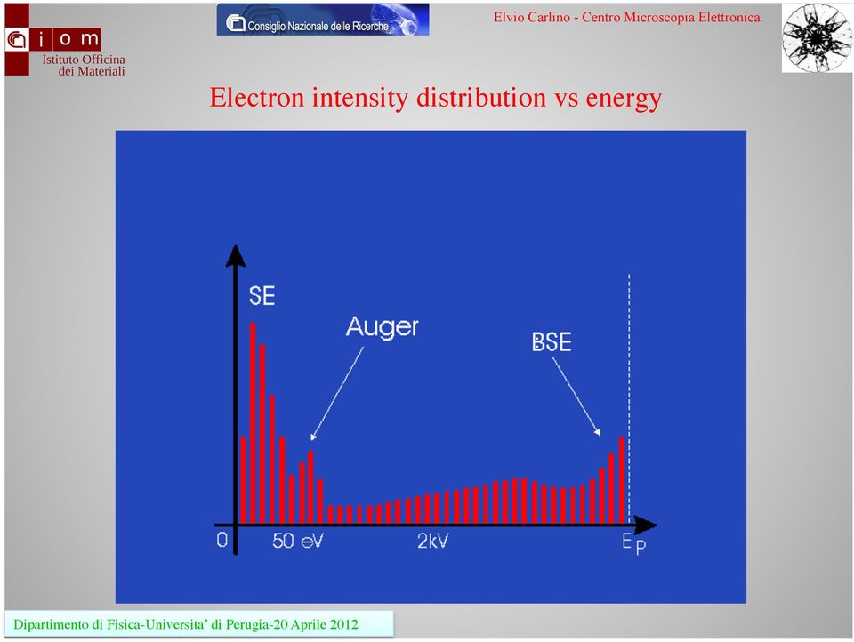
13 Electron intensity distribution vs energy
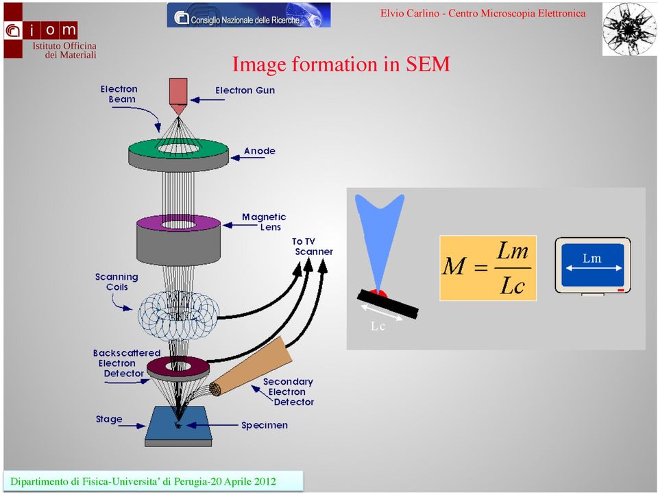
14 Image formation in SEM
15 Cross section secondary electrons (SE) Q SE (E SE ) = n c e 4 k 3 F A 3πEρN 0 (E SE E F ) 2 Differential cross section of low energy secondary electrons Q SE is in terms of secondary electrons per unit energy interval per incident electron per (atom/cm 2 ) k F is the magnitude of the wave-vector corresponding to the Fermi energy E F A is the atomic weight, n c is the number of conduction-band electrons ρ is the material density E SE is the secondary electron energy E is the beam energy

16 Cross section back-scattered electrons (BSE) Rutheford differential cross section for elastic scattering vsscattering angle θ for a constant value of the electron energy E: dq(θ ) = e 4 Z 2 16(4πε 0 E) 2 dω [sin 2 (θ / 2) + θ 0 2 / 4)] 2 dω = 2πsinθdθ Solid angle into which the electron of energy E is scattered at an angle θ from its incident direction e is the electronic charge Z is the atomic number of the scattering atom ε 0 is the dielectric constant (θ 0 /2) 2 is the screening parameter
 2 is the screening")
17 Signals generated by primary electrons

18 Interaction volume Secondary X-ray fluorescence Auger electrons 1 nm secondary electrons 5-50 nm Back-scattered electrons 1-2µm Characteristic X-ray 2-5µm bremsstrahlung

19 Interaction volume vs HV&Z Low Z High Z Tilt angle Up: high accelerating voltage Down: low accelerating voltage

20 SE yeld vs thickness

21 BSE coefficient vs Z
22 Spatial distribution of the back-scattered electrons
23 SE & BSE coefficients vs Z
24 SE: surface and depth of field Elvio Carlino - Centro Microscopia Elettronica
25 SE & BSE Topography Composition
26 Elvio Carlino - Centro Microscopia Elettronica Tungsten with Titanium and Titanium Nitride Al Ti W
27 Example EBSD
28 Low energy imaging of insulator
29 Imaging at low energy HT
30 Imaging at low energy HT
31 Nanotubes
32 American Journal of Physics 1976 Physics world 2002
33 STEM in SEM
34 Set up for STEM imaging in SEM
35 S(T)EM image
36 S(T)EM in biology
37 ???
38 Lattice fringes by diffractive imaging in SEM
39 Low voltage ~ 100 ev
40 Summary SEM is a powerful and flexible tool to study inorganic and organic matter at nanometer resolution, and more. In many cases the images reveals the specimen properties in an intuitive way giving access to quantitative morphology, crystal structure, chemistry, etc.. It is worthwhile to underline how electron microscopy also represents a flexible tool that can be tuned to design new experiments to access subtle properties of the electron matter interaction paving the way to the knowledge of new science.
41 Nobody can resist to electron microscopy!
Electron Microscopy SEM and TEM
 Electron Microscopy SEM and TEM Content 1. Introduction: Motivation for electron microscopy 2. Interaction with matter 3. SEM: Scanning Electron Microscopy 3.1 Functional Principle 3.2 Examples 3.3 EDX
Nanoelectronics 09. Atsufumi Hirohata Department of Electronics. Quick Review over the Last Lecture
 Nanoelectronics 09 Atsufumi Hirohata Department of Electronics 12:00 Wednesday, 4/February/2015 (P/L 006) Quick Review over the Last Lecture ( Field effect transistor (FET) ): ( Drain ) current increases
Electron Microscopy 3. SEM. Image formation, detection, resolution, signal to noise ratio, interaction volume, contrasts
 Electron Microscopy 3. SEM Image formation, detection, resolution, signal to noise ratio, interaction volume, contrasts 3-1 SEM is easy! Just focus and shoot "Photo"!!! Please comment this picture... Any
View of ΣIGMA TM (Ref. 1)
") Overview of the FESEM system 1. Electron optical column 2. Specimen chamber 3. EDS detector [Electron Dispersive Spectroscopy] 4. Monitors 5. BSD (Back scatter detector) 6. Personal Computer 7. ON/STANDBY/OFF
Overview of the FESEM system 1. Electron optical column 2. Specimen chamber 3. EDS detector [Electron Dispersive Spectroscopy] 4. Monitors 5. BSD (Back scatter detector) 6. Personal Computer 7. ON/STANDBY/OFF
Preface Light Microscopy X-ray Diffraction Methods
 Preface xi 1 Light Microscopy 1 1.1 Optical Principles 1 1.1.1 Image Formation 1 1.1.2 Resolution 3 1.1.3 Depth of Field 5 1.1.4 Aberrations 6 1.2 Instrumentation 8 1.2.1 Illumination System 9 1.2.2 Objective
Chapter 14 High Resolution TEM
 Chapter 14 High Resolution TEM K. Ishizuka (1980) Contrast Transfer of Crystal Images in TEM, Ultramicroscopy 5,pages 55-65. L. Reimer (1993) Transmission Electron Microscopy, Springer Verlag, Berlin.
7. advanced SEM. Latest generation of SEM SEM
 7. advanced SEM SEM Low voltage SE imaging Condition of the surface, coatings, plasma cleaning Low voltage BSE imaging Polishing for BSE, EDX and EBSD, effect of ion beam etching/polishing 1 Latest generation
Optical Microscope; Scanning Electron Microscope (SEM); Transmission Electron Microscope (TEM);
; Transmission Electron Microscope (TEM);") Lecture 3 Brief Overview of Traditional Microscopes Optical Microscope; Scanning Electron Microscope (SEM); Transmission Electron Microscope (TEM); Comparison with scanning probe microscope (SPM) General
Lecture 3 Brief Overview of Traditional Microscopes Optical Microscope; Scanning Electron Microscope (SEM); Transmission Electron Microscope (TEM); Comparison with scanning probe microscope (SPM) General
Nanometer-scale imaging and metrology, nano-fabrication with the Orion Helium Ion Microscope
 [email protected] Nanometer-scale imaging and metrology, nano-fabrication with the Orion Helium Ion Microscope Bin Ming, András E. Vladár and Michael T. Postek National Institute of Standards and Technology
Electron Microscopy 3. SEM. Image formation, detection, resolution, signal to noise ratio, interaction volume, contrasts
 Electron Microscopy 3. SEM Image formation, detection, resolution, signal to noise ratio, interaction volume, contrasts SEM is easy! Just focus and shoot "Photo"!!! Please comment this picture... Any idea
Scanning Electron Microscopy Primer
 Scanning Electron Microscopy Primer Bob Hafner This primer is intended as background for the Introductory Scanning Electron Microscopy training offered by the University of Minnesota s Characterization
Properties of Electrons, their Interactions with Matter and Applications in Electron Microscopy
 Properties of Electrons, their Interactions with Matter and Applications in Electron Microscopy By Frank Krumeich Laboratory of Inorganic Chemistry, ETH Zurich, Vladimir-Prelog-Weg 1, 8093 Zurich, Switzerland
The Basics of Scanning Electron Microscopy
 The Basics of Scanning Electron Microscopy The small scanning electron microscope is easy to use because almost every variable is pre-set: the acceleration voltage is always 15kV, it has only a single
Reflection Electron Microscopy and Spectroscopy for Surface Analysis
 Reflection Electron Microscopy and Spectroscopy for Surface Analysis by Zhong Lin Wang 1 Introduction In 1986, E. Ruska was awarded the Nobel Physics Prize for his pioneering work of building the world's
Lenses and Apertures of A TEM
 Instructor: Dr. C.Wang EMA 6518 Course Presentation Lenses and Apertures of A TEM Group Member: Anup Kr. Keshri Srikanth Korla Sushma Amruthaluri Venkata Pasumarthi Xudong Chen Outline Electron Optics
EDS system. CRF Oxford Instruments INCA CRF EDAX Genesis EVEX- NanoAnalysis Table top system
 EDS system Most common X-Ray measurement system in the SEM lab. Major elements (10 wt% or greater) identified in ~10 secs. Minor elements identifiable in ~100 secs. Rapid qualitative and accurate quantitative
SILA Sistema Integrato di Laboratori per l Ambiente. CENTRE FOR MICROSCOPY AND MICROANALYSIS Scientific coordinator: Prof.ssa Rosanna De Rosa
 CENTRE FOR MICROSCOPY AND MICROANALYSIS Scientific coordinator: Prof.ssa Rosanna De Rosa 0 The Centre for Microscopy and Microanalysis (CM2) is an interdisciplinary service centre, a comprehensive suite
PHYSICAL METHODS, INSTRUMENTS AND MEASUREMENTS Vol. III - Surface Characterization - Marie-Geneviève Barthés-Labrousse
 SURFACE CHARACTERIZATION Marie-Geneviève Centre d Etudes de Chimie Métallurgique, CNRS, Vitry-sur-Seine, France Keywords: Surface Analysis, Surface imaging, Surface composition, Surface chemical analysis,
Fundamentals of Scanning Electron Microscopy
 1 Fundamentals of Scanning Electron Microscopy Weilie Zhou, Robert P. Apkarian, Zhong Lin Wang, and David Joy 1. Introduction The scanning electron microscope (SEM) is one of the most versatile instruments
Measuring the Point Spread Function of a Fluorescence Microscope
 Frederick National Laboratory Measuring the Point Spread Function of a Fluorescence Microscope Stephen J Lockett, PhD Principal Scientist, Optical Microscopy and Analysis Laboratory Frederick National
Introduction to EDX. Energy Dispersive X-ray Microanalysis (EDS, Energy dispersive Spectroscopy) Basics of EDX
 Basics of EDX") Introduction to EDX Energy Dispersive X-ray Microanalysis (EDS, Energy dispersive Spectroscopy) EDX Marco Cantoni 1 Basics of EDX a) Generation of X-rays b) Detection Si(Li) Detector, SDD Detector, EDS
Introduction to EDX Energy Dispersive X-ray Microanalysis (EDS, Energy dispersive Spectroscopy) EDX Marco Cantoni 1 Basics of EDX a) Generation of X-rays b) Detection Si(Li) Detector, SDD Detector, EDS
CALCULATION METHODS OF X-RAY SPECTRA: A COMPARATIVE STUDY
 243 CALCULATION METHODS OF X-RAY SPECTRA: A COMPARATIVE STUDY B. Chyba, M. Mantler, H. Ebel, R. Svagera Technische Universit Vienna, Austria ABSTRACT The accurate characterization of the spectral distribution
The Focused Ion Beam Scanning Electron Microscope: A tool for sample preparation, two and three dimensional imaging. Jacob R.
 The Focused Ion Beam Scanning Electron Microscope: A tool for sample preparation, two and three dimensional imaging Jacob R. Bowen Contents Components of a FIB-SEM Ion interactions Deposition & patterns
CSCI 4974 / 6974 Hardware Reverse Engineering. Lecture 8: Microscopy and Imaging
 CSCI 4974 / 6974 Hardware Reverse Engineering Lecture 8: Microscopy and Imaging Data Acquisition for RE Microscopy Imaging Registration and stitching Microscopy Optical Electron Scanning Transmission Scanning
Microscopy. MICROSCOPY Light Electron Tunnelling Atomic Force RESOLVE: => INCREASE CONTRAST BIODIVERSITY I BIOL1051 MAJOR FUNCTIONS OF MICROSCOPES
 BIODIVERSITY I BIOL1051 Microscopy Professor Marc C. Lavoie [email protected] MAJOR FUNCTIONS OF MICROSCOPES MAGNIFY RESOLVE: => INCREASE CONTRAST Microscopy 1. Eyepieces 2. Diopter adjustment
Scanning Electron Microscopy tools for material characterization
 5th International Workshop on Mechanisms of Vacuum Arcs 02-04/09/2015 Scanning Electron Microscopy tools for material characterization Focus on EBSD for characterisation of dislocation structures Floriane
Phase Characterization of TiO 2 Powder by XRD and TEM
 Kasetsart J. (Nat. Sci.) 42 : 357-361 (28) Phase Characterization of TiO 2 Powder by XRD and TEM Kheamrutai Thamaphat 1 *, Pichet Limsuwan 1 and Boonlaer Ngotawornchai 2 ABSTRACT In this study, the commercial
Looking through the fish-eye the Electron Ronchigram. Duncan T.L. Alexander CIME seminar May 24, 2012
 Looking through the fish-eye the Electron Ronchigram Duncan T.L. Alexander CIME seminar May 24, 2012 Introduction Aim of the seminar: open a discussion on the Electron Ronchigram How is it formed? What
bulk 5. Surface Analysis Why surface Analysis? Introduction Methods: XPS, AES, RBS
 5. Surface Analysis Introduction Methods: XPS, AES, RBS Autumn 2011 Experimental Methods in Physics Marco Cantoni Why surface Analysis? Bulk: structural function Electrical/thermal conduction Volume increases
Near-field scanning optical microscopy (SNOM)
") Adviser: dr. Maja Remškar Institut Jožef Stefan January 2010 1 2 3 4 5 6 Fluorescence Raman and surface enhanced Raman 7 Conventional optical microscopy-limited resolution Two broad classes of techniques
Adviser: dr. Maja Remškar Institut Jožef Stefan January 2010 1 2 3 4 5 6 Fluorescence Raman and surface enhanced Raman 7 Conventional optical microscopy-limited resolution Two broad classes of techniques
Scanning Electron Microscopy Services for Pharmaceutical Manufacturers
 Scanning Electron Microscopy Services for Pharmaceutical Manufacturers Author: Gary Brake, Marketing Manager Date: August 1, 2013 Analytical Testing Laboratory www.atl.semtechsolutions.com Scanning Electron
Scanning He + Ion Beam Microscopy and Metrology. David C Joy University of Tennessee, and Oak Ridge National Laboratory
 Scanning He + Ion Beam Microscopy and Metrology David C Joy University of Tennessee, and Oak Ridge National Laboratory The CD-SEM For thirty years the CD-SEM has been the tool for metrology But now, as
NATIONAL NETWORK OF ELECTRON MICROSCOPY RNME. NETWORK MANAGEMENT MODEL a ARTICULATION AND GENERAL OPERATION. (English translation draft)
") NATIONAL NETWORK OF ELECTRON MICROSCOPY RNME NETWORK MANAGEMENT MODEL a ARTICULATION AND GENERAL OPERATION (English translation draft) 1. Introduction 2 2. Objectives 2 3. Constitution 2 4. Organization
NATIONAL NETWORK OF ELECTRON MICROSCOPY RNME NETWORK MANAGEMENT MODEL a ARTICULATION AND GENERAL OPERATION (English translation draft) 1. Introduction 2 2. Objectives 2 3. Constitution 2 4. Organization
Basic principles and mechanisms of NSOM; Different scanning modes and systems of NSOM; General applications and advantages of NSOM.
 Lecture 16: Near-field Scanning Optical Microscopy (NSOM) Background of NSOM; Basic principles and mechanisms of NSOM; Basic components of a NSOM; Different scanning modes and systems of NSOM; General
PHOTOELECTRIC EFFECT AND DUAL NATURE OF MATTER AND RADIATIONS
 PHOTOELECTRIC EFFECT AND DUAL NATURE OF MATTER AND RADIATIONS 1. Photons 2. Photoelectric Effect 3. Experimental Set-up to study Photoelectric Effect 4. Effect of Intensity, Frequency, Potential on P.E.
for Low power Energy Harvesting Sun to fiber' Solar Devices
 Nanostructured Energy Conversion for Low power Energy Harvesting Devices and Beyond for High power Sun to fiber' Solar Devices Michael Oye and Nobuhiko Nobby Kobayashi Advanced Studies Laboratories and
Microscopy and Nanoindentation. Combining Orientation Imaging. to investigate localized. deformation behaviour. Felix Reinauer
 Combining Orientation Imaging Microscopy and Nanoindentation to investigate localized deformation behaviour Felix Reinauer René de Kloe Matt Nowell Introduction Anisotropy in crystalline materials Presentation
h e l p s y o u C O N T R O L
 contamination analysis for compound semiconductors ANALYTICAL SERVICES B u r i e d d e f e c t s, E v a n s A n a l y t i c a l g r o u p h e l p s y o u C O N T R O L C O N T A M I N A T I O N Contamination
CHAPTER - 1. Chapter ONE: WAVES CHAPTER - 2. Chapter TWO: RAY OPTICS AND OPTICAL INSTRUMENTS. CHAPTER - 3 Chapter THREE: WAVE OPTICS PERIODS PERIODS
 BOARD OF INTERMEDIATE EDUCATION, A.P., HYDERABAD REVISION OF SYLLABUS Subject PHYSICS-II (w.e.f 2013-14) Chapter ONE: WAVES CHAPTER - 1 1.1 INTRODUCTION 1.2 Transverse and longitudinal waves 1.3 Displacement
Name: Due: September 21 st 2012. Physics 7230 Laboratory 3: High Resolution SEM Imaging
 Name: Due: September 21 st 2012 Physics 7230 Laboratory 3: High Resolution SEM Imaging 1. What is meant by the term resolution? How does this differ from other image variables, such as signal to noise
Diffraction Course Series 2015
 Diffraction Course Series 2015 Mark Wainwright Analytical Centre Kensington Campus, Chemical Sciences Building F10, Room G37 The Mark Wainwright Analytical Centre is offering a new series of courses covering
Lecture 6 Scanning Tunneling Microscopy (STM) General components of STM; Tunneling current; Feedback system; Tip --- the probe.
 General components of STM; Tunneling current; Feedback system; Tip --- the probe.") Lecture 6 Scanning Tunneling Microscopy (STM) General components of STM; Tunneling current; Feedback system; Tip --- the probe. Brief Overview of STM Inventors of STM The Nobel Prize in Physics 1986 Nobel
Lecture 6 Scanning Tunneling Microscopy (STM) General components of STM; Tunneling current; Feedback system; Tip --- the probe. Brief Overview of STM Inventors of STM The Nobel Prize in Physics 1986 Nobel
Introduction to Energy Dispersive X-ray Spectrometry (EDS)
") Introduction to Energy Dispersive X-ray Spectrometry (EDS) 1. Introduction 1.1 Principles of the technique EDS makes use of the X-ray spectrum emitted by a solid sample bombarded with a focused beam of
Introduction to Energy Dispersive X-ray Spectrometry (EDS) 1. Introduction 1.1 Principles of the technique EDS makes use of the X-ray spectrum emitted by a solid sample bombarded with a focused beam of
Raman spectroscopy Lecture
 Raman spectroscopy Lecture Licentiate course in measurement science and technology Spring 2008 10.04.2008 Antti Kivioja Contents - Introduction - What is Raman spectroscopy? - The theory of Raman spectroscopy
Microscopy: Principles and Advances
 Microscopy: Principles and Advances Chandrashekhar V. Kulkarni University of Central Lancashire, Preston, United kingdom May, 2014 University of Ljubljana Academic Background 2005-2008: PhD-Chemical Biology
Use the BET (after Brunauer, Emmett and Teller) equation is used to give specific surface area from the adsorption
 equation is used to give specific surface area from the adsorption") Number of moles of N 2 in 0.129dm 3 = 0.129/22.4 = 5.76 X 10⁻³ moles of N 2 gas Module 8 : Surface Chemistry Objectives Lecture 37 : Surface Characterization Techniques After studying this lecture, you
Number of moles of N 2 in 0.129dm 3 = 0.129/22.4 = 5.76 X 10⁻³ moles of N 2 gas Module 8 : Surface Chemistry Objectives Lecture 37 : Surface Characterization Techniques After studying this lecture, you
Physical Properties and Functionalization of Low-Dimensional Materials
 Physical Properties and Functionalization of Low-Dimensional Materials Physics Department, University of Trieste Graduate School of Physics, XXVI cycle Supervisor: Co-supervisor: Prof. Alessandro BARALDI
Ion Beam Sputtering: Practical Applications to Electron Microscopy
 Ion Beam Sputtering: Practical Applications to Electron Microscopy Applications Laboratory Report Introduction Electron microscope specimens, both scanning (SEM) and transmission (TEM), often require a
How To Understand Light And Color
 PRACTICE EXAM IV P202 SPRING 2004 1. In two separate double slit experiments, an interference pattern is observed on a screen. In the first experiment, violet light (λ = 754 nm) is used and a second-order
Physics 30 Worksheet # 14: Michelson Experiment
 Physics 30 Worksheet # 14: Michelson Experiment 1. The speed of light found by a Michelson experiment was found to be 2.90 x 10 8 m/s. If the two hills were 20.0 km apart, what was the frequency of the
Status of the FERMI@Elettra Free Electron Laser
 Status of the FERMI@Elettra Free Electron Laser E. Allaria on behalf of the FERMI team Work partially supported by the Italian Ministry of University and Research under grants FIRB-RBAP045JF2 and FIRB-RBAP06AWK3
X-Ray Diffraction HOW IT WORKS WHAT IT CAN AND WHAT IT CANNOT TELL US. Hanno zur Loye
 X-Ray Diffraction HOW IT WORKS WHAT IT CAN AND WHAT IT CANNOT TELL US Hanno zur Loye X-rays are electromagnetic radiation of wavelength about 1 Å (10-10 m), which is about the same size as an atom. The
Secondary Ion Mass Spectrometry
 Secondary Ion Mass Spectrometry A PRACTICAL HANDBOOK FOR DEPTH PROFILING AND BULK IMPURITY ANALYSIS R. G. Wilson Hughes Research Laboratories Malibu, California F. A. Stevie AT&T Bell Laboratories Allentown,
Electron Microprobe Analysis X-ray spectrometry:
 Electron Microprobe Analysis X-ray spectrometry: 1. X-ray generation and emission 2. X-ray detection and measurement X-ray energy and wavelength E=hν h : Planck's constant (6.626x10⁻³⁴ Joule.sec or, 6.626x10⁻³⁴
Fast Varifocal Lenses Based on KTa 1-x Nb x O 3 (KTN) Single Crystals
 Single Crystals") : Crystal Technologies Fast Varifocal Lenses Based on KTa 1-x Nb x O 3 () Single Crystals Tadayuki Imai, Shogo Yagi, Seiji Toyoda, and Masahiro Sasaura Abstract NTT Photonics Laboratories has recently
: Crystal Technologies Fast Varifocal Lenses Based on KTa 1-x Nb x O 3 () Single Crystals Tadayuki Imai, Shogo Yagi, Seiji Toyoda, and Masahiro Sasaura Abstract NTT Photonics Laboratories has recently
Lecture 20: Scanning Confocal Microscopy (SCM) Rationale for SCM. Principles and major components of SCM. Advantages and major applications of SCM.
 Rationale for SCM. Principles and major components of SCM. Advantages and major applications of SCM.") Lecture 20: Scanning Confocal Microscopy (SCM) Rationale for SCM. Principles and major components of SCM. Advantages and major applications of SCM. Some limitations (disadvantages) of NSOM A trade-off
Lecture 20: Scanning Confocal Microscopy (SCM) Rationale for SCM. Principles and major components of SCM. Advantages and major applications of SCM. Some limitations (disadvantages) of NSOM A trade-off
NEAR FIELD OPTICAL MICROSCOPY AND SPECTROSCOPY WITH STM AND AFM PROBES
 Vol. 93 (1997) A CTA PHYSICA POLONICA A No. 2 Proceedings of the 1st International Symposium on Scanning Probe Spectroscopy and Related Methods, Poznań 1997 NEAR FIELD OPTICAL MICROSCOPY AND SPECTROSCOPY
Defect studies of optical materials using near-field scanning optical microscopy and spectroscopy
 UCRL-ID-142178 Defect studies of optical materials using near-field scanning optical microscopy and spectroscopy M. Yan, J. McWhirter, T. Huser, W. Siekhaus January, 2001 U.S. Department of Energy Laboratory
Crystal Structure of High Temperature Superconductors. Marie Nelson East Orange Campus High School NJIT Professor: Trevor Tyson
 Crystal Structure of High Temperature Superconductors Marie Nelson East Orange Campus High School NJIT Professor: Trevor Tyson Introduction History of Superconductors Superconductors are material which
Physics 441/2: Transmission Electron Microscope
 Physics 441/2: Transmission Electron Microscope Introduction In this experiment we will explore the use of transmission electron microscopy (TEM) to take us into the world of ultrasmall structures. This
Usage of Carbon Nanotubes in Scanning Probe Microscopes as Probe. Keywords: Carbon Nanotube, Scanning Probe Microscope
 International Journal of Arts and Sciences 3(1): 18-26 (2009) CD-ROM. ISSN: 1944-6934 InternationalJournal.org Usage of Carbon Nanotubes in Scanning Probe Microscopes as Probe Bedri Onur Kucukyildirim,
Microscopic Techniques
 Microscopic Techniques Outline 1. Optical microscopy Conventional light microscopy, Fluorescence microscopy, confocal/multiphoton microscopy and Stimulated emission depletion microscopy 2. Scanning probe
Lectures about XRF (X-Ray Fluorescence)
") 1 / 38 Lectures about XRF (X-Ray Fluorescence) Advanced Physics Laboratory Laurea Magistrale in Fisica year 2013 - Camerino 2 / 38 X-ray Fluorescence XRF is an acronym for X-Ray Fluorescence. The XRF technique
1 / 38 Lectures about XRF (X-Ray Fluorescence) Advanced Physics Laboratory Laurea Magistrale in Fisica year 2013 - Camerino 2 / 38 X-ray Fluorescence XRF is an acronym for X-Ray Fluorescence. The XRF technique
Jorge E. Fernández Laboratory of Montecuccolino (DIENCA), Alma Mater Studiorum University of Bologna, via dei Colli, 16, 40136 Bologna, Italy
, Alma Mater Studiorum University of Bologna, via dei Colli, 16, 40136 Bologna, Italy") Information technology (IT) for teaching X- and gamma-ray transport: the computer codes MUPLOT and SHAPE, and the web site dedicated to photon transport Jorge E. Fernández Laboratory of Montecuccolino
Information technology (IT) for teaching X- and gamma-ray transport: the computer codes MUPLOT and SHAPE, and the web site dedicated to photon transport Jorge E. Fernández Laboratory of Montecuccolino
Optical Coherence Tomography OCT. 3D Imaging in Medical Technology and Quality Control
 Optical Coherence Tomography OCT 3D Imaging in Medical Technology and Quality Control SLN Seminar, EPMT Lausanne, 26. May. 2011 Ch. Meier www.optolab.ch 1 / 27 SLN/EPMT, Lausanne, 26.5.2011 Ch. Meier Outline
PHYS 222 Spring 2012 Final Exam. Closed books, notes, etc. No electronic device except a calculator.
 PHYS 222 Spring 2012 Final Exam Closed books, notes, etc. No electronic device except a calculator. NAME: (all questions with equal weight) 1. If the distance between two point charges is tripled, the
Calibration of AFM with virtual standards; robust, versatile and accurate. Richard Koops VSL Dutch Metrology Institute Delft
 Calibration of AFM with virtual standards; robust, versatile and accurate Richard Koops VSL Dutch Metrology Institute Delft 19-11-2015 VSL Dutch Metrology Institute VSL is the national metrology institute
Energy Dispersive Spectroscopy on the SEM: A Primer
 Energy Dispersive Spectroscopy on the SEM: A Primer Bob Hafner This primer is intended as background for the EDS Analysis on the SEM course offered by the University of Minnesota s Characterization Facility.
X-ray diffraction techniques for thin films
 X-ray diffraction techniques for thin films Rigaku Corporation Application Laboratory Takayuki Konya 1 Today s contents (PM) Introduction X-ray diffraction method Out-of-Plane In-Plane Pole figure Reciprocal
Powder diffraction and synchrotron radiation
 Powder diffraction and synchrotron radiation Gilberto Artioli Dip. Geoscienze UNIPD CIRCe Center for Cement Materials single xl diffraction powder diffraction Ideal powder Powder averaging Textured sample
STAR: State of the art
 i n v e s t i a m o n e l v o s t r o f u t u r o STAR: State of the art Raffaele G. Agostino PON MaTeRiA Materials and Technologies for Advanced Research MaTeRiA EU/National Funding PON Ricerca e Competititvità
Laue lens for Nuclear Medicine
 Laue lens for Nuclear Medicine PhD in Physics Gianfranco Paternò Ferrara, 6-11-013 Supervisor: prof. Vincenzo Guidi Sensors and Semiconductors Lab, Department of Physics and Earth Science, University of
COMPARISON OF FOUR DATA ANALYSIS SOFTWARE FOR COMBINED X-RAY REFLECTIVITY AND GRAZING INCIDENCE X-RAY FLUORESCENCE MEASUREMENTS
 COMPARISON OF FOUR DATA ANALYSIS SOFTWARE FOR COMBINED X-RAY REFLECTIVITY AND GRAZING INCIDENCE X-RAY FLUORESCENCE MEASUREMENTS Bérenger Caby (1), Fabio Brigidi (2), Dieter Ingerle (3), Blanka Detlefs
Confocal Microscopy and Atomic Force Microscopy (AFM) A very brief primer...
 A very brief primer...") Confocal Microscopy and Atomic Force Microscopy (AFM) of biofilms A very brief primer... Fundamentals of Confocal Microscopy Based on a conventional fluorescence microscope Fluorescent Microscope Confocal
Confocal Microscopy and Atomic Force Microscopy (AFM) of biofilms A very brief primer... Fundamentals of Confocal Microscopy Based on a conventional fluorescence microscope Fluorescent Microscope Confocal
Transmission Electron Microscopy
 Transmission Electron Microscopy Wacek Swiech, Honghui Zhou, Jim Mabon, Changqiang (CQ) Chen and Matt Bresin Frederick Seitz Materials Research Laboratory University of Illinois at Urbana-Champaign Outline
Introduction to the Scanning Electron Microscope
 Introduction to the Scanning Electron Microscope Theory, Practice, & Procedures Prepared by Michael Dunlap & Dr. J. E. Adaskaveg Presented by the FACILITY FOR ADVANCED INSTRUMENTATION, U. C. Davis 1997
PHYSICS PAPER 1 (THEORY)
") PHYSICS PAPER 1 (THEORY) (Three hours) (Candidates are allowed additional 15 minutes for only reading the paper. They must NOT start writing during this time.) ---------------------------------------------------------------------------------------------------------------------
PHYSICS PAPER 1 (THEORY) (Three hours) (Candidates are allowed additional 15 minutes for only reading the paper. They must NOT start writing during this time.) ---------------------------------------------------------------------------------------------------------------------
Usage of AFM, SEM and TEM for the research of carbon nanotubes
 Usage of AFM, SEM and TEM for the research of carbon nanotubes K.Safarova *1, A.Dvorak 2, R. Kubinek 1, M.Vujtek 1, A. Rek 3 1 Department of Experimental Physics, Faculty of Science, Palacky University,
- particle with kinetic energy E strikes a barrier with height U 0 > E and width L. - classically the particle cannot overcome the barrier
 Tunnel Effect: - particle with kinetic energy E strikes a barrier with height U 0 > E and width L - classically the particle cannot overcome the barrier - quantum mechanically the particle can penetrated
ORIENTATION CHARACTERISTICS OF THE MICROSTRUCTURE OF MATERIALS
 ORIENTATION CHARACTERISTICS OF THE MICROSTRUCTURE OF MATERIALS K. Sztwiertnia Polish Academy of Sciences, Institute of Metallurgy and Materials Science, 25 Reymonta St., 30-059 Krakow, Poland MMN 2009
Near-field optics and plasmonics
 Near-field optics and plasmonics Manuel Rodrigues Gonçalves AFM topography 10 Pol. y / (µm) 8 6 4 2 0 0 2 4 6 x / (µm) 8 10 nm 60 80 100 120 140 Physik M. Sc. Master Advanced Materials Winter semester
DURABILITY OF MORTAR LININGS IN DUCTILE IRON PIPES Durability of mortar linings
 DURABILITY OF MORTAR LININGS IN DUCTILE IRON PIPES Durability of mortar linings I. S. MELAND SINTEF Civil and Environmental Engineering, Cement and Concrete, Trondheim, Norway Durability of Building Materials
Spectral distribution from end window X-ray tubes
 Copyright (C) JCPDS-International Centre for Diffraction Data 1999 393 Spectral distribution from end window X-ray tubes N. Broll 1, P. de Chateaubourg 2 1 FORTEX - E.N.S.A.I.S. 24, bld de la Victoire,
Chapter 4. Microscopy, Staining, and Classification. Lecture prepared by Mindy Miller-Kittrell North Carolina State University
 Chapter 4 Microscopy, Staining, and Classification 2012 Pearson Education Inc. Lecture prepared by Mindy Miller-Kittrell North Carolina State University Microscopy and Staining 2012 Pearson Education Inc.
Tecnai on-line help Working with a FEG 1 FEG_A4.doc Software version 2
 Tecnai on-line help Working with a FEG 1 Tecnai on-line help manual -- Working with a FEG Table of Contents 1 Introduction...2 2 FEG Safety...2 2.1 The column valves...2 3 FEG States...3 4 Starting the
ULTRAFAST LASERS: Free electron lasers thrive from synergy with ultrafast laser systems
 Page 1 of 6 ULTRAFAST LASERS: Free electron lasers thrive from synergy with ultrafast laser systems Free electron lasers support unique time-resolved experiments over a wide range of x-ray wavelengths,
Revision problem. Chapter 18 problem 37 page 612. Suppose you point a pinhole camera at a 15m tall tree that is 75m away.
 Revision problem Chapter 18 problem 37 page 612 Suppose you point a pinhole camera at a 15m tall tree that is 75m away. 1 Optical Instruments Thin lens equation Refractive power Cameras The human eye Combining
EXPERIMENTAL CONDITIONS FOR CROSS SECTION MEASUREMENTS FOR ANALYTICAL PURPOSES. L. Csedreki 1. Abstract. I. Introduction
 ACTA PHYSICA DEBRECINA XLVI, 25 (2012) EXPERIMENTAL CONDITIONS FOR CROSS SECTION MEASUREMENTS FOR ANALYTICAL PURPOSES L. Csedreki 1 1 Institute of Nuclear Research of the Hungarian Academy of Sciences,
CREOL, College of Optics & Photonics, University of Central Florida
 OSE6650 - Optical Properties of Nanostructured Materials Optical Properties of Nanostructured Materials Fall 2013 Class 3 slide 1 Challenge: excite and detect the near field Thus far: Nanostructured materials
www.keithley.com 1 st Edition Nanotechnology Measurement Handbook A Guide to Electrical Measurements for Nanoscience Applications
 www.keithley.com 1 st Edition Nanotechnology Measurement Handbook A Guide to Electrical Measurements for Nanoscience Applications To get a free electronic version of this book, visit Keithley s Knowledge
Chapter 1 High-Resolution Optical and Confocal Microscopy
 Chapter 1 High-Resolution Optical and Confocal Microscopy Olaf Hollricher and Wolfram Ibach Abstract In this chapter, the theory of optical image formation in an optical microscope is described, and the
Application Note # EDS-10 Advanced light element and low energy X-ray analysis of a TiB 2 TiC SiC ceramic material using EDS spectrum imaging
 Quantitative analysis Ceramics sample Peak deconvolution EDS map Phase analysis Application Note # EDS-10 Advanced light element and low energy X-ray analysis of a TiB 2 TiC SiC ceramic material using
Electron spectroscopy Lecture 1-21. Kai M. Siegbahn (1918 - ) Nobel Price 1981 High resolution Electron Spectroscopy
 Nobel Price 1981 High resolution Electron Spectroscopy") Electron spectroscopy Lecture 1-21 Kai M. Siegbahn (1918 - ) Nobel Price 1981 High resolution Electron Spectroscopy 653: Electron Spectroscopy urse structure cture 1. Introduction to electron spectroscopies
Electron spectroscopy Lecture 1-21 Kai M. Siegbahn (1918 - ) Nobel Price 1981 High resolution Electron Spectroscopy 653: Electron Spectroscopy urse structure cture 1. Introduction to electron spectroscopies
CASINO V2.42 A Fast and Easy-to-use Modeling Tool for Scanning Electron Microscopy and Microanalysis Users
 SCANNING VOL. 29, 92 11 (27) Wiley Periodicals, Inc. CASINO V2.42 A Fast and Easy-to-use Modeling Tool for Scanning Electron Microscopy and Microanalysis Users DOMINIQUE DROUIN 1,ALEXANDRE RÉAL COUTURE
Supporting Information
 Supporting Information Simple and Rapid Synthesis of Ultrathin Gold Nanowires, Their Self-Assembly and Application in Surface-Enhanced Raman Scattering Huajun Feng, a Yanmei Yang, a Yumeng You, b Gongping
APPLICATION OF X-RAY COMPUTED TOMOGRAPHY IN SILICON SOLAR CELLS
 APPLICATION OF X-RAY COMPUTED TOMOGRAPHY IN SILICON SOLAR CELLS V.A. Popovich 1, W. Verwaal 2, M. Janssen 1, I. J. Bennett 3, I.M.Richardson 1, 1. Delft University of Technology, Department of Materials
Forensic Science: The Basics. Microscopy
 Forensic Science: The Basics Microscopy Chapter 6 Jay A. Siegel,Ph.D. Power point presentation by Greg Galardi, Peru State College, Peru Nebraska Presentation by Greg Galardi, Peru State College CRC Press,
VECTORIAL ELECTRIC FIELD MONTE CARO SIMULA- TIONS FOR FOCUSED LASER BEAMS (800 nm 2220 nm) IN A BIOLOGICAL SAMPLE
 IN A BIOLOGICAL SAMPLE") Progress In Electromagnetics Research, Vol. 142, 667 681, 2013 VECTORIAL ELECTRIC FIELD MONTE CARO SIMULA- TIONS FOR FOCUSED LASER BEAMS (800 nm 2220 nm) IN A BIOLOGICAL SAMPLE Fuhong Cai 1, Jiaxin Yu
Progress In Electromagnetics Research, Vol. 142, 667 681, 2013 VECTORIAL ELECTRIC FIELD MONTE CARO SIMULA- TIONS FOR FOCUSED LASER BEAMS (800 nm 2220 nm) IN A BIOLOGICAL SAMPLE Fuhong Cai 1, Jiaxin Yu