7. advanced SEM. Latest generation of SEM SEM
|
|
|
- Beverley Johnson
- 10 years ago
- Views:
Transcription
1 7. advanced SEM SEM Low voltage SE imaging Condition of the surface, coatings, plasma cleaning Low voltage BSE imaging Polishing for BSE, EDX and EBSD, effect of ion beam etching/polishing 1 Latest generation of SEM Field emission gun monochromators beam boosters, beam deceleration, Lens-design: In-lens, Semi-inlens, immersion lens Short working distance Résolution (nm) Basse low voltage, tension/haute high resolution: résolution: - observation Observation de of la surface the real réelle surface - échantillons Non-metallic non-métallisés samples - faible Reduced endommagement beam damagedû au faisceau Haute High tension/haute voltage, résolution: - effets high de resolution: bord - détails Edge fins effects non-résolus FE - fort endommagement Charging effectsdû au faisceau Beam damage 1985 LaB 6 W Detectors: Everhard-Thornley (SE) In-column (through the lens, inlens, in-beam ) Low Voltage BSE detection, energy filtering (separation of materials and topography contrast) Tension d'accélération (kv) Analytical SEM: SDD EDX detectors (high throughput, large collection angle) High-speed EBSD detectors Beam currents of several 100 na 2

2 SEM low kv imaging No specimen preparation needed: Low kv imaging of non-conducting, low density samples Al2O3 Nanocrystals FEI Magellan Operator: Ingo Gestmann Samples: Marco Cantoni 3 SEM low kv imaging No specimen preparation needed: Low kv imaging of non-conducting, low density samples Carbon nano-tubes (MWCT) FEI Magellan Operator: Ingo Gestmann Samples: Marco Cantoni 4

3 SEM low kv imaging No specimen preparation needed: Low kv imaging of non-conducting samples Liquid filled organic membranes Zeiss Nvision 40 Marco Cantoni 5 SEM low kv imaging No specimen preparation needed: Low kv imaging of non-conducting samples Liquid filled organic membranes Zeiss Nvision 40 Marco Cantoni 6

4 SEM low kv imaging Purely organic specimen: non-conductive, low density: Metal coating 15nm Ag/Pd coating 3nm Os coating HeLa Cells, Graham Knott Marco Cantoni, Nvision 40 7 SEM low kv imaging Easy sample: SC wire Nb 3 Sn in Cu matrix 8

5 SEM low kv imaging Easy samples: Everhard-Thornley detector (SE) Solid state BSE detector 9 SEM low kv BSE imaging 2keV, In-Column EsB detector Solid state BSE detector 10

6 SEM low kv imaging Easy samples: 11 SEM low kv imaging Easy samples: 12

7 SEM low kv imaging Easy samples: 13 SEM low kv imaging Contamination by hydro-carbons contamination spoils imaging at low kv How to avoid (at CIME): plasma cleaning of the sample before inserting Plasma clean the chamber at each insertion (multi-user environment) XL30 FEG & EVACTRON NVision40 & EVACTRON 14
 XL30 FEG & EVACTRON NVision40 &")
8 SEM: Preparation for analytical EM Nb 3 Sn multifilament superconducting cable 0.5 mm Nb 3 Sn superconductor multifilament cable: Nb 3 Sn filaments (diameter ~5um) in bronze matrix Solid State BSE detector 20kV acceleration voltage EDX maps Sn Cu Mechanical polishing <-> Ar ion beam polished Nb 15 Mechanical polishing: Grains of harder phase incorporated in softer matrix Deformed microstructure at surface reduces formation of Kikichi lines in EBSD SEM BSE/EDX/EBSD After Ar ion polishing (Gatan PIPS) Sn Cu Nb 16

9 Ion polishing in-chamber ET-detector SE in-column InLens SE-detector in-column, energy-selective EsB BSE-detector 17 SEM low kv BSE imaging Nb 3 Sn multifilament Superconductors Materials & orientation contrast 5µm NVision kV EsB detector 18

10 FIB/SEM low kv BSE imaging Nb 3 Sn multifilament Superconductors Materials & orientation contrast 19 SEM preparation: polishing Goal of final polishing: Removal of the damaged surface layer mechano-chemical polishing (EBSD) or ion polishing 5kV 1kV 30kV escape depth of BSE: Nb 3 Sn 30kV: 800nm 5kV: 50nm 1kV: < 5nm Interaction volume Blue: scattered electrons Red: backscattered electrons (leaving the sample surface) Monte-Carlo Simulation CASINO v
 Monte-Carlo Simulation")
11 New HR-SEM at CIME Starting point: XL-30 SFEG SIRION (since 2001) First semi-in-lens HR-SEM: in-lens (through the lens) detection of SE and BSE Resolution in UHR mode: 1.5 nm at 10 kv (or higher); 2.5 nm at 1 kv 21 22
; 2.")
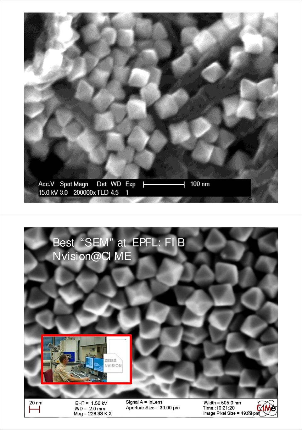
12 23 Best SEM at EPFL: FIB 24
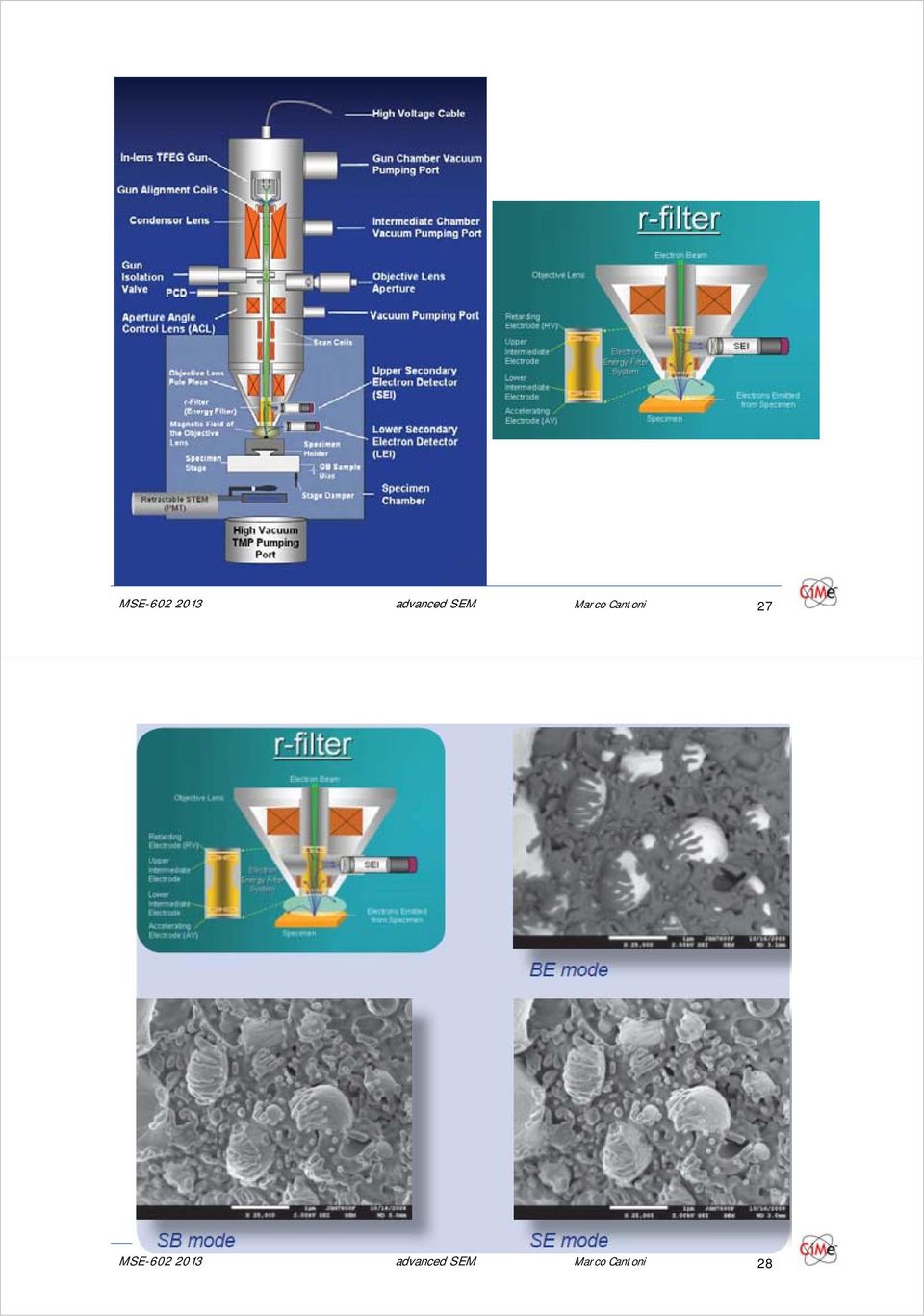
13 Two different contrasts with one scan: parallel detectors 25 26

14 27 28
15 29 30

16 31 MERLIN Introducing... Analytical power for the sub-nanometer world 32

17 MERLIN Analytical power for the sub-nanometer world High stability field emitter cathode Maximum probe current 300 na Beam Double Booster condenser lens Brightness Aperture independent of the electron probe probe current adjustment maintained for low landing energies Energy selective Backscatter detector (EsB) In-lens Secondary Electron detector GEMINI II final lens GEMINI II design Complete detection system Proven GEMINI final lens design New double condenser lens for highest probe current possibilities (300 na) Beam booster technology maintains brightness of all electron probes including low landing energies True on-axis in-lens SE and BSE detectors 33 34
 Beam booster technology maintains brightness of all electron probes including low landing energies True on-axis in-lens SE and BSE detectors 33")
18 MERLIN Analytical power for the sub-nanometer world In-lens SE (Secondary Electron detector) Topographical information with on-axis in-lens SE detector system GEMINI II design Complete detection Complete detection system: Unique double in-lens detection Acquisition of pure secondary and backscatter electron signals Separation of compositional, topographical and crystalline surface information 35 MERLIN Analytical power for the sub-nanometer world Energy filtering grid EsB (Energy selective Backscatter detector) Compositional contrast with on-axis in column EsB detector Si 3 N 4 TiN Si Ti system GEMINI II design Complete detection Complete detection system: Unique double in-lens detection Acquisition of pure secondary and backscatter electron signals Separation of compositional, topographical and crystalline surface information 36

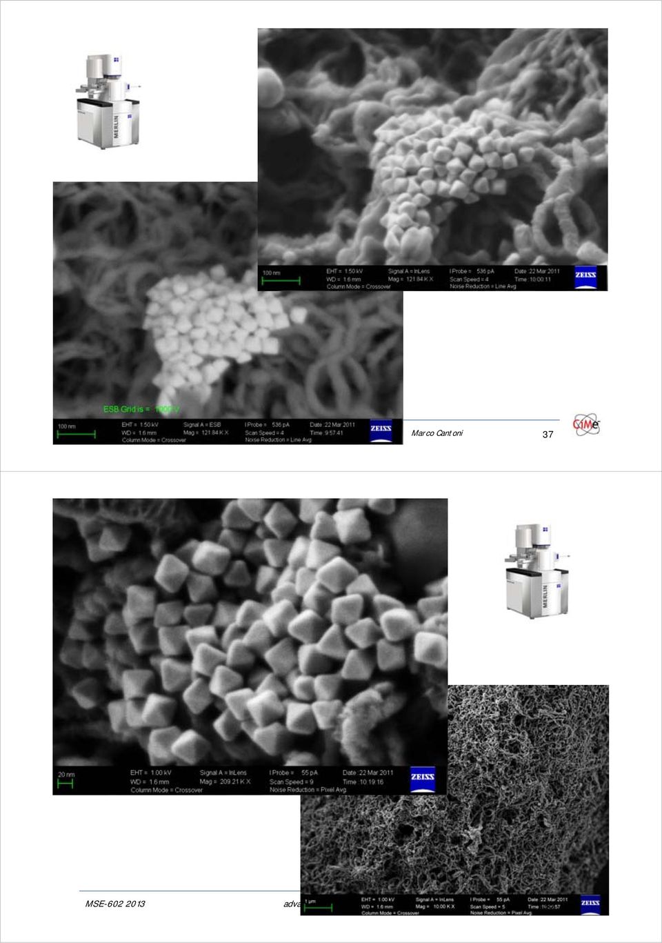
19 37 38
20 39 40

21 41 42
22 43 44
23 45 Sapphire 46
Electron Microscopy 3. SEM. Image formation, detection, resolution, signal to noise ratio, interaction volume, contrasts
 Electron Microscopy 3. SEM Image formation, detection, resolution, signal to noise ratio, interaction volume, contrasts 3-1 SEM is easy! Just focus and shoot "Photo"!!! Please comment this picture... Any
Electron Microscopy 3. SEM. Image formation, detection, resolution, signal to noise ratio, interaction volume, contrasts
 Electron Microscopy 3. SEM Image formation, detection, resolution, signal to noise ratio, interaction volume, contrasts SEM is easy! Just focus and shoot "Photo"!!! Please comment this picture... Any idea
View of ΣIGMA TM (Ref. 1)
") Overview of the FESEM system 1. Electron optical column 2. Specimen chamber 3. EDS detector [Electron Dispersive Spectroscopy] 4. Monitors 5. BSD (Back scatter detector) 6. Personal Computer 7. ON/STANDBY/OFF
Overview of the FESEM system 1. Electron optical column 2. Specimen chamber 3. EDS detector [Electron Dispersive Spectroscopy] 4. Monitors 5. BSD (Back scatter detector) 6. Personal Computer 7. ON/STANDBY/OFF
12. FIB. Marco Cantoni 021/693.48.16. Centre Interdisciplinaire de Microscopie Electronique CIME. Focused Ion Beam
 12. FIB Marco Cantoni 021/693.48.16 Centre Interdisciplinaire de Microscopie Electronique CIME 1 Focused Ion Beam a) Principles How does it work..? Ion source, optics, interaction with the sample b) Basic
Nanometer-scale imaging and metrology, nano-fabrication with the Orion Helium Ion Microscope
 [email protected] Nanometer-scale imaging and metrology, nano-fabrication with the Orion Helium Ion Microscope Bin Ming, András E. Vladár and Michael T. Postek National Institute of Standards and Technology
Basics of Image and data analysis in 3D
 Basics of Image and data analysis in 3D outline Why image processing, and how? Image processing in 2D What is an ideal image? Histogram tells stories! Before taking the image: the right imaging conditions!
The Basics of Scanning Electron Microscopy
 The Basics of Scanning Electron Microscopy The small scanning electron microscope is easy to use because almost every variable is pre-set: the acceleration voltage is always 15kV, it has only a single
3D EDX MICROANALYSIS IN A FIB/SEM:
 3D EDX MICROANALYSIS IN A FIB/SEM: WHAT CAN WE EXPECT, WHERE ARE THE LIMITS...? Marco Cantoni, Pierre Burdet Centre Interdisciplinaire de Microscopie Electronique (EPFL-CIME) CIME Since August 2008: Nvision
The Focused Ion Beam Scanning Electron Microscope: A tool for sample preparation, two and three dimensional imaging. Jacob R.
 The Focused Ion Beam Scanning Electron Microscope: A tool for sample preparation, two and three dimensional imaging Jacob R. Bowen Contents Components of a FIB-SEM Ion interactions Deposition & patterns
Ion Beam Sputtering: Practical Applications to Electron Microscopy
 Ion Beam Sputtering: Practical Applications to Electron Microscopy Applications Laboratory Report Introduction Electron microscope specimens, both scanning (SEM) and transmission (TEM), often require a
Microscopy and Nanoindentation. Combining Orientation Imaging. to investigate localized. deformation behaviour. Felix Reinauer
 Combining Orientation Imaging Microscopy and Nanoindentation to investigate localized deformation behaviour Felix Reinauer René de Kloe Matt Nowell Introduction Anisotropy in crystalline materials Presentation
Name: Due: September 21 st 2012. Physics 7230 Laboratory 3: High Resolution SEM Imaging
 Name: Due: September 21 st 2012 Physics 7230 Laboratory 3: High Resolution SEM Imaging 1. What is meant by the term resolution? How does this differ from other image variables, such as signal to noise
Scanning Electron Microscopy: an overview on application and perspective
 Scanning Electron Microscopy: an overview on application and perspective Elvio Carlino Center for Electron Microscopy - IOM-CNR Laboratorio Nazionale TASC - Trieste, Italy Location of the Center for Electron
Demonstration of sub-4 nm nanoimprint lithography using a template fabricated by helium ion beam lithography
 Demonstration of sub-4 nm nanoimprint lithography using a template fabricated by helium ion beam lithography Wen-Di Li*, Wei Wu** and R. Stanley Williams Hewlett-Packard Labs *Current address: University
Electron Microscopy SEM and TEM
 Electron Microscopy SEM and TEM Content 1. Introduction: Motivation for electron microscopy 2. Interaction with matter 3. SEM: Scanning Electron Microscopy 3.1 Functional Principle 3.2 Examples 3.3 EDX
Scanning Electron Microscopy Primer
 Scanning Electron Microscopy Primer Bob Hafner This primer is intended as background for the Introductory Scanning Electron Microscopy training offered by the University of Minnesota s Characterization
Scanning Electron Microscopy tools for material characterization
 5th International Workshop on Mechanisms of Vacuum Arcs 02-04/09/2015 Scanning Electron Microscopy tools for material characterization Focus on EBSD for characterisation of dislocation structures Floriane
Usage of AFM, SEM and TEM for the research of carbon nanotubes
 Usage of AFM, SEM and TEM for the research of carbon nanotubes K.Safarova *1, A.Dvorak 2, R. Kubinek 1, M.Vujtek 1, A. Rek 3 1 Department of Experimental Physics, Faculty of Science, Palacky University,
Nanoelectronics 09. Atsufumi Hirohata Department of Electronics. Quick Review over the Last Lecture
 Nanoelectronics 09 Atsufumi Hirohata Department of Electronics 12:00 Wednesday, 4/February/2015 (P/L 006) Quick Review over the Last Lecture ( Field effect transistor (FET) ): ( Drain ) current increases
Micro-CT for SEM Non-destructive Measurement and Volume Visualization of Specimens Internal Microstructure in SEM Micro-CT Innovation with Integrity
 Micro-CT for SEM Non-destructive Measurement and Volume Visualization of Specimens Internal Microstructure in SEM Innovation with Integrity Micro-CT 3D Microscopy Using Micro-CT for SEM Micro-CT for SEM
Microscopy. MICROSCOPY Light Electron Tunnelling Atomic Force RESOLVE: => INCREASE CONTRAST BIODIVERSITY I BIOL1051 MAJOR FUNCTIONS OF MICROSCOPES
 BIODIVERSITY I BIOL1051 Microscopy Professor Marc C. Lavoie [email protected] MAJOR FUNCTIONS OF MICROSCOPES MAGNIFY RESOLVE: => INCREASE CONTRAST Microscopy 1. Eyepieces 2. Diopter adjustment
h e l p s y o u C O N T R O L
 contamination analysis for compound semiconductors ANALYTICAL SERVICES B u r i e d d e f e c t s, E v a n s A n a l y t i c a l g r o u p h e l p s y o u C O N T R O L C O N T A M I N A T I O N Contamination
Coating Thickness and Composition Analysis by Micro-EDXRF
 Application Note: XRF Coating Thickness and Composition Analysis by Micro-EDXRF www.edax.com Coating Thickness and Composition Analysis by Micro-EDXRF Introduction: The use of coatings in the modern manufacturing
FEI Forensic Systems. Choose your armory for the next decade
 FEI Forensic Systems Choose your armory for the next decade 1 Choose your armory for the next decade Forensic Quanta High vacuum, low vacuum and environmental SEM (ESEM ) GSR S50 SEM for automated analysis
Scanning He + Ion Beam Microscopy and Metrology. David C Joy University of Tennessee, and Oak Ridge National Laboratory
 Scanning He + Ion Beam Microscopy and Metrology David C Joy University of Tennessee, and Oak Ridge National Laboratory The CD-SEM For thirty years the CD-SEM has been the tool for metrology But now, as
Modification of Pd-H 2 and Pd-D 2 thin films processed by He-Ne laser
 Modification of Pd-H 2 and Pd-D 2 thin films processed by He-Ne laser V.Nassisi #, G.Caretto #, A. Lorusso #, D.Manno %, L.Famà %, G.Buccolieri %, A.Buccolieri %, U.Mastromatteo* # Laboratory of Applied
bulk 5. Surface Analysis Why surface Analysis? Introduction Methods: XPS, AES, RBS
 5. Surface Analysis Introduction Methods: XPS, AES, RBS Autumn 2011 Experimental Methods in Physics Marco Cantoni Why surface Analysis? Bulk: structural function Electrical/thermal conduction Volume increases
ORIENTATION CHARACTERISTICS OF THE MICROSTRUCTURE OF MATERIALS
 ORIENTATION CHARACTERISTICS OF THE MICROSTRUCTURE OF MATERIALS K. Sztwiertnia Polish Academy of Sciences, Institute of Metallurgy and Materials Science, 25 Reymonta St., 30-059 Krakow, Poland MMN 2009
Preface Light Microscopy X-ray Diffraction Methods
 Preface xi 1 Light Microscopy 1 1.1 Optical Principles 1 1.1.1 Image Formation 1 1.1.2 Resolution 3 1.1.3 Depth of Field 5 1.1.4 Aberrations 6 1.2 Instrumentation 8 1.2.1 Illumination System 9 1.2.2 Objective
Lenses and Apertures of A TEM
 Instructor: Dr. C.Wang EMA 6518 Course Presentation Lenses and Apertures of A TEM Group Member: Anup Kr. Keshri Srikanth Korla Sushma Amruthaluri Venkata Pasumarthi Xudong Chen Outline Electron Optics
Fundamentals of Scanning Electron Microscopy
 1 Fundamentals of Scanning Electron Microscopy Weilie Zhou, Robert P. Apkarian, Zhong Lin Wang, and David Joy 1. Introduction The scanning electron microscope (SEM) is one of the most versatile instruments
CALCULATION METHODS OF X-RAY SPECTRA: A COMPARATIVE STUDY
 243 CALCULATION METHODS OF X-RAY SPECTRA: A COMPARATIVE STUDY B. Chyba, M. Mantler, H. Ebel, R. Svagera Technische Universit Vienna, Austria ABSTRACT The accurate characterization of the spectral distribution
Lecture 6 Scanning Tunneling Microscopy (STM) General components of STM; Tunneling current; Feedback system; Tip --- the probe.
 General components of STM; Tunneling current; Feedback system; Tip --- the probe.") Lecture 6 Scanning Tunneling Microscopy (STM) General components of STM; Tunneling current; Feedback system; Tip --- the probe. Brief Overview of STM Inventors of STM The Nobel Prize in Physics 1986 Nobel
Lecture 6 Scanning Tunneling Microscopy (STM) General components of STM; Tunneling current; Feedback system; Tip --- the probe. Brief Overview of STM Inventors of STM The Nobel Prize in Physics 1986 Nobel
NATIONAL NETWORK OF ELECTRON MICROSCOPY RNME. NETWORK MANAGEMENT MODEL a ARTICULATION AND GENERAL OPERATION. (English translation draft)
") NATIONAL NETWORK OF ELECTRON MICROSCOPY RNME NETWORK MANAGEMENT MODEL a ARTICULATION AND GENERAL OPERATION (English translation draft) 1. Introduction 2 2. Objectives 2 3. Constitution 2 4. Organization
NATIONAL NETWORK OF ELECTRON MICROSCOPY RNME NETWORK MANAGEMENT MODEL a ARTICULATION AND GENERAL OPERATION (English translation draft) 1. Introduction 2 2. Objectives 2 3. Constitution 2 4. Organization
Introduction to the Scanning Electron Microscope
 Introduction to the Scanning Electron Microscope Theory, Practice, & Procedures Prepared by Michael Dunlap & Dr. J. E. Adaskaveg Presented by the FACILITY FOR ADVANCED INSTRUMENTATION, U. C. Davis 1997
SEM/FIB Workbench. Klocke Nanotechnik. Microtechnology Network. Motion from the Nanoworld. One of 279 members in a. Pascalstr. 17 Aachen, Germany
 Intro_0 SEM/FIB Workbench Motion from the Nanoworld One of 279 members in a Pascalstr. 17 Aachen, Germany Microtechnology Network Centimeter Stroke Atomic Resolution Modular Nanorobotics Modular Nanorobotics
Keywords: Planar waveguides, sol-gel technology, transmission electron microscopy
 Structural and optical characterisation of planar waveguides obtained via Sol-Gel F. Rey-García, C. Gómez-Reino, M.T. Flores-Arias, G.F. De La Fuente, W. Assenmacher, W. Mader ABSTRACT Planar waveguides
Usage of Carbon Nanotubes in Scanning Probe Microscopes as Probe. Keywords: Carbon Nanotube, Scanning Probe Microscope
 International Journal of Arts and Sciences 3(1): 18-26 (2009) CD-ROM. ISSN: 1944-6934 InternationalJournal.org Usage of Carbon Nanotubes in Scanning Probe Microscopes as Probe Bedri Onur Kucukyildirim,
EDS system. CRF Oxford Instruments INCA CRF EDAX Genesis EVEX- NanoAnalysis Table top system
 EDS system Most common X-Ray measurement system in the SEM lab. Major elements (10 wt% or greater) identified in ~10 secs. Minor elements identifiable in ~100 secs. Rapid qualitative and accurate quantitative
Institute s brochure. Microstructure Analysis, Metallography and Mechanical Testing of Materials. Institute of Materials Research
 Institute s brochure Microstructure Analysis, Metallography and Mechanical Testing of Materials Institute of Materials Research Micro structure Analysis and Metallography is one of the core teams of the
Application Note # EDS-10 Advanced light element and low energy X-ray analysis of a TiB 2 TiC SiC ceramic material using EDS spectrum imaging
 Quantitative analysis Ceramics sample Peak deconvolution EDS map Phase analysis Application Note # EDS-10 Advanced light element and low energy X-ray analysis of a TiB 2 TiC SiC ceramic material using
Carl Zeiss NTS - Nano Technology System Division. ΣIGMA Field Emission Scanning Electron Microscope. Instruction Manual. Enabling the Nano-Age World
 Carl Zeiss NTS - Nano Technology System Division ΣIGMA Field Emission Scanning Electron Microscope Instruction Manual Enabling the Nano-Age World Operator s User Guide ΣIGMA FESEM Original instructions
Displays. Cathode Ray Tube. Semiconductor Elements. Basic applications. Oscilloscope TV Old monitors. 2009, Associate Professor PhD. T.
 Displays Semiconductor Elements 1 Cathode Ray Tube Basic applications Oscilloscope TV Old monitors 2 1 Idea of Electrostatic Deflection 3 Inside an Electrostatic Deflection Cathode Ray Tube Gun creates
Electron Microprobe Analysis X-ray spectrometry:
 Electron Microprobe Analysis X-ray spectrometry: 1. X-ray generation and emission 2. X-ray detection and measurement X-ray energy and wavelength E=hν h : Planck's constant (6.626x10⁻³⁴ Joule.sec or, 6.626x10⁻³⁴
CSCI 4974 / 6974 Hardware Reverse Engineering. Lecture 8: Microscopy and Imaging
 CSCI 4974 / 6974 Hardware Reverse Engineering Lecture 8: Microscopy and Imaging Data Acquisition for RE Microscopy Imaging Registration and stitching Microscopy Optical Electron Scanning Transmission Scanning
Principles of Ion Implant
 Principles of Ion Implant Generation of ions dopant gas containing desired species BF 3, B 2 H 6, PH 3, AsH 3, AsF 5 plasma provides positive ions (B 11 ) +, BF 2+, (P 31 ) +, (P 31 ) ++ Ion Extraction
Lectures about XRF (X-Ray Fluorescence)
") 1 / 38 Lectures about XRF (X-Ray Fluorescence) Advanced Physics Laboratory Laurea Magistrale in Fisica year 2013 - Camerino 2 / 38 X-ray Fluorescence XRF is an acronym for X-Ray Fluorescence. The XRF technique
1 / 38 Lectures about XRF (X-Ray Fluorescence) Advanced Physics Laboratory Laurea Magistrale in Fisica year 2013 - Camerino 2 / 38 X-ray Fluorescence XRF is an acronym for X-Ray Fluorescence. The XRF technique
Introduction to Energy Dispersive X-ray Spectrometry (EDS)
") Introduction to Energy Dispersive X-ray Spectrometry (EDS) 1. Introduction 1.1 Principles of the technique EDS makes use of the X-ray spectrum emitted by a solid sample bombarded with a focused beam of
Introduction to Energy Dispersive X-ray Spectrometry (EDS) 1. Introduction 1.1 Principles of the technique EDS makes use of the X-ray spectrum emitted by a solid sample bombarded with a focused beam of
Forensic Science: The Basics. Microscopy
 Forensic Science: The Basics Microscopy Chapter 6 Jay A. Siegel,Ph.D. Power point presentation by Greg Galardi, Peru State College, Peru Nebraska Presentation by Greg Galardi, Peru State College CRC Press,
Coating Technology: Evaporation Vs Sputtering
 Satisloh Italy S.r.l. Coating Technology: Evaporation Vs Sputtering Gianni Monaco, PhD R&D project manager, Satisloh Italy 04.04.2016 V1 The aim of this document is to provide basic technical information
PHYSICAL METHODS, INSTRUMENTS AND MEASUREMENTS Vol. III - Surface Characterization - Marie-Geneviève Barthés-Labrousse
 SURFACE CHARACTERIZATION Marie-Geneviève Centre d Etudes de Chimie Métallurgique, CNRS, Vitry-sur-Seine, France Keywords: Surface Analysis, Surface imaging, Surface composition, Surface chemical analysis,
Wafer Manufacturing. Reading Assignments: Plummer, Chap 3.1~3.4
 Wafer Manufacturing Reading Assignments: Plummer, Chap 3.1~3.4 1 Periodic Table Roman letters give valence of the Elements 2 Why Silicon? First transistor, Shockley, Bardeen, Brattain1947 Made by Germanium
Introduktion til røntgenfluorescens (XRF) og skanning elektron mikroskopi (SEM) Michelle Taube Nationalmuseet Bevaringsafdelingen
 og skanning elektron mikroskopi (SEM) Michelle Taube Nationalmuseet Bevaringsafdelingen") Introduktion til røntgenfluorescens (XRF) og skanning elektron mikroskopi (SEM) Michelle Taube Nationalmuseet Bevaringsafdelingen Introduktion til røntgenfluorescens (XRF) og skanning elektron mikroskopi
Introduktion til røntgenfluorescens (XRF) og skanning elektron mikroskopi (SEM) Michelle Taube Nationalmuseet Bevaringsafdelingen Introduktion til røntgenfluorescens (XRF) og skanning elektron mikroskopi
Supporting Information
 Supporting Information Simple and Rapid Synthesis of Ultrathin Gold Nanowires, Their Self-Assembly and Application in Surface-Enhanced Raman Scattering Huajun Feng, a Yanmei Yang, a Yumeng You, b Gongping
Mass production, R&D Failure analysis. Fault site pin-pointing (EM, OBIRCH, FIB, etc. ) Bottleneck Physical science analysis (SEM, TEM, Auger, etc.
 Bottleneck Physical science analysis (SEM, TEM, Auger, etc.") Failure Analysis System for Submicron Semiconductor Devices 68 Failure Analysis System for Submicron Semiconductor Devices Munetoshi Fukui Yasuhiro Mitsui, Ph. D. Yasuhiko Nara Fumiko Yano, Ph. D. Takashi
Failure Analysis System for Submicron Semiconductor Devices 68 Failure Analysis System for Submicron Semiconductor Devices Munetoshi Fukui Yasuhiro Mitsui, Ph. D. Yasuhiko Nara Fumiko Yano, Ph. D. Takashi
Vacuum Evaporation Recap
 Sputtering Vacuum Evaporation Recap Use high temperatures at high vacuum to evaporate (eject) atoms or molecules off a material surface. Use ballistic flow to transport them to a substrate and deposit.
Dual Beam FIB/FEG Microscope
 INVITATION FOR TENDER FOR SUPPLY OF EQUIPMENT Sealed tender offers are invited in two separate sealed covers (Technical and Commercial offers) from eligible manufacturers/suppliers or their direct Indian
Graphical displays are generally of two types: vector displays and raster displays. Vector displays
 Display technology Graphical displays are generally of two types: vector displays and raster displays. Vector displays Vector displays generally display lines, specified by their endpoints. Vector display
Optical Microscope; Scanning Electron Microscope (SEM); Transmission Electron Microscope (TEM);
; Transmission Electron Microscope (TEM);") Lecture 3 Brief Overview of Traditional Microscopes Optical Microscope; Scanning Electron Microscope (SEM); Transmission Electron Microscope (TEM); Comparison with scanning probe microscope (SPM) General
Lecture 3 Brief Overview of Traditional Microscopes Optical Microscope; Scanning Electron Microscope (SEM); Transmission Electron Microscope (TEM); Comparison with scanning probe microscope (SPM) General
THERMO NORAN SYSTEM SIX ENERGY DISPERSIVE X- RAY SPECTROMETER. Insert Nickname Here. Operating Instructions
 THERMO NORAN SYSTEM SIX ENERGY DISPERSIVE X- RAY SPECTROMETER Insert Nickname Here Operating Instructions Table of Contents 1 INTRODUCTION Safety 1 Samples 1 2 BACKGROUND Background Information 3 References
TOF FUNDAMENTALS TUTORIAL
 TOF FUNDAMENTALS TUTORIAL Presented By: JORDAN TOF PRODUCTS, INC. 990 Golden Gate Terrace Grass Valley, CA 95945 530-272-4580 / 530-272-2955 [fax] www.rmjordan.com [web] [email protected] [e-mail] This
LASER ENGRAVING REFLECTIVE METALS TO CREATE SCANNER READABLE BARCODES Paper P516
 LASER ENGRAVING REFLECTIVE METALS TO CREATE SCANNER READABLE BARCODES Paper P516 Paul M Harrison, Jozef Wendland, Matthew Henry Powerlase Ltd, Imperial House, Link 10, Napier Way, Crawley, West Sussex,
Evaluation of combined EBIC/FIB methods for solar cell characterization
 Evaluation of combined EBIC/FIB methods for solar cell characterization Frank Altmann*, Jan Schischka*, Vinh Van Ngo**, Laurens F. Tz. Kwakman**, Ralf Lehmann** *Fraunhofer Insitute for Mechanics of Materials
Testing and characterization of anti-reflection coatings on glass
 Testing and characterization of anti-reflection coatings on glass Diagnostic approaches at CSP M.Turek, M. Dyrba, S. Großer, V. Naumann, Ch. Hagendorf contact: [email protected] Tests and methods
EDXRF of Used Automotive Catalytic Converters
 EDXRF of Used Automotive Catalytic Converters Energy Dispersive X-Ray Fluorescence (EDXRF) is a very powerful technique for measuring the concentration of elements in a sample. It is fast, nondestructive,
CONCEPT OF DETERMINISTIC ION IMPLANTATION AT THE NANOSCALE
 CONCEPT OF DETERMINISTIC ION IMPLANTATION AT THE NANOSCALE Daniel Spemann Jan Meijer 1, Jürgen W. Gerlach, Paul Räcke 1, Susann Liedtke, Stephan Rauschenbach 2, Bernd Rauschenbach 1 University of Leipzig,
X-ray diffraction techniques for thin films
 X-ray diffraction techniques for thin films Rigaku Corporation Application Laboratory Takayuki Konya 1 Today s contents (PM) Introduction X-ray diffraction method Out-of-Plane In-Plane Pole figure Reciprocal
Laser beam sintering of coatings and structures
 Laser beam sintering of coatings and structures Anne- Maria Reinecke, Peter Regenfuß, Maren Nieher, Sascha Klötzer, Robby Ebert, Horst Exner Laserinstitut Mittelsachsen e.v. an der Hochschule Mittweida,
LIFE SCIENCE I TECHNICAL BULLETIN ISSUE N 11 /JULY 2008
 LIFE SCIENCE I TECHNICAL BULLETIN ISSUE N 11 /JULY 2008 PARTICLE CHARACTERISATION IN EXCIPIENTS, DRUG PRODUCTS AND DRUG SUBSTANCES AUTHOR: HILDEGARD BRÜMMER, PhD, CUSTOMER SERVICE MANAGER, SGS LIFE SCIENCE
Measuring the Point Spread Function of a Fluorescence Microscope
 Frederick National Laboratory Measuring the Point Spread Function of a Fluorescence Microscope Stephen J Lockett, PhD Principal Scientist, Optical Microscopy and Analysis Laboratory Frederick National
Diagnostics. Electric probes. Instituto de Plasmas e Fusão Nuclear Instituto Superior Técnico Lisbon, Portugal http://www.ipfn.ist.utl.
 C. Silva Lisboa, Jan. 2014 IST Diagnostics Electric probes Instituto de Plasmas e Fusão Nuclear Instituto Superior Técnico Lisbon, Portugal http://www.ipfn.ist.utl.pt Langmuir probes Simplest diagnostic
Lateral Resolution of EDX Analysis with Low Acceleration Voltage SEM
 Original Paper Lateral Resolution of EDX Analysis with Low Acceleration Voltage SEM Satoshi Hashimoto 1, Tsuguo Sakurada 1, and Minoru Suzuki 2 1 JFE-Techno research corporation, 1-1 Minamiwatarida, Kawasaki,
Laue lens for Nuclear Medicine
 Laue lens for Nuclear Medicine PhD in Physics Gianfranco Paternò Ferrara, 6-11-013 Supervisor: prof. Vincenzo Guidi Sensors and Semiconductors Lab, Department of Physics and Earth Science, University of
Raman spectroscopy Lecture
 Raman spectroscopy Lecture Licentiate course in measurement science and technology Spring 2008 10.04.2008 Antti Kivioja Contents - Introduction - What is Raman spectroscopy? - The theory of Raman spectroscopy
INTRODUCTION TO THE XL30-FEG SEM. 1.1 The mouse. 1.2. The monitor. Figure 1.1 1. THE USER INTERFACE
 INTRODUCTION TO THE XL30-FEG SEM All software used to control the microscope runs in the MS-Windows environment. This environment is loaded on the Windows2000 operating system. However, it is not really
APPLICATION OF X-RAY COMPUTED TOMOGRAPHY IN SILICON SOLAR CELLS
 APPLICATION OF X-RAY COMPUTED TOMOGRAPHY IN SILICON SOLAR CELLS V.A. Popovich 1, W. Verwaal 2, M. Janssen 1, I. J. Bennett 3, I.M.Richardson 1, 1. Delft University of Technology, Department of Materials
Precision Miniature Load Cell. Models 8431, 8432 with Overload Protection
 w Technical Product Information Precision Miniature Load Cell with Overload Protection 1. Introduction The load cells in the model 8431 and 8432 series are primarily designed for the measurement of force
How To Analyze Plasma With An Inductively Coupled Plasma Mass Spectrometer
 What is ICP-MS? and more importantly, what can it do? Inductively Coupled Plasma Mass Spectrometry or ICP-MS is an analytical technique used for elemental determinations. The technique was commercially
Project 2B Building a Solar Cell (2): Solar Cell Performance
: Solar Cell Performance") April. 15, 2010 Due April. 29, 2010 Project 2B Building a Solar Cell (2): Solar Cell Performance Objective: In this project we are going to experimentally measure the I-V characteristics, energy conversion
April. 15, 2010 Due April. 29, 2010 Project 2B Building a Solar Cell (2): Solar Cell Performance Objective: In this project we are going to experimentally measure the I-V characteristics, energy conversion
Secondary Ion Mass Spectrometry
 Secondary Ion Mass Spectrometry A PRACTICAL HANDBOOK FOR DEPTH PROFILING AND BULK IMPURITY ANALYSIS R. G. Wilson Hughes Research Laboratories Malibu, California F. A. Stevie AT&T Bell Laboratories Allentown,
Introduction to EDX. Energy Dispersive X-ray Microanalysis (EDS, Energy dispersive Spectroscopy) Basics of EDX
 Basics of EDX") Introduction to EDX Energy Dispersive X-ray Microanalysis (EDS, Energy dispersive Spectroscopy) EDX Marco Cantoni 1 Basics of EDX a) Generation of X-rays b) Detection Si(Li) Detector, SDD Detector, EDS
Introduction to EDX Energy Dispersive X-ray Microanalysis (EDS, Energy dispersive Spectroscopy) EDX Marco Cantoni 1 Basics of EDX a) Generation of X-rays b) Detection Si(Li) Detector, SDD Detector, EDS
Development of on line monitor detectors used for clinical routine in proton and ion therapy
 Development of on line monitor detectors used for clinical routine in proton and ion therapy A. Ansarinejad Torino, february 8 th, 2010 Overview Hadrontherapy CNAO Project Monitor system: Part1:preliminary
STM and AFM Tutorial. Katie Mitchell January 20, 2010
 STM and AFM Tutorial Katie Mitchell January 20, 2010 Overview Scanning Probe Microscopes Scanning Tunneling Microscopy (STM) Atomic Force Microscopy (AFM) Contact AFM Non-contact AFM RHK UHV350 AFM/STM
X-RAY TUBE SELECTION CRITERIA FOR BGA / CSP X-RAY INSPECTION
 X-RAY TUBE SELECTION CRITERIA FOR BGA / CSP X-RAY INSPECTION David Bernard Dage Precision Industries Inc. Fremont, California [email protected] ABSTRACT The x-ray inspection of PCB assembly processes
Proceedings of the Sixth Workshop on RF Superconductivity, CEBAF, Newport News, Virginia, USA
 FIELD EMISSION IN RF CAVITIES : OBSERVATION OF LIGHT SPOTS AT HIGH ELECTRIC FIELDS T. Junquera, A. Le Goff Institut de Physique Nucleaire (CNRS-IN2P3) 91406 Orsay France B. Bonin, H. Safa, J. Tan DSM/DAPNIA/SEA
Objectives 200 CHAPTER 4 RESISTANCE
 Objectives Explain the differences among conductors, insulators, and semiconductors. Define electrical resistance. Solve problems using resistance, voltage, and current. Describe a material that obeys
VCR Ion Beam Sputter Coater
 VCR Ion Beam Sputter Coater Sputtering Process and Rates 2 Vacuum System 3 Loading the Sputter Chamber 4 Sputter Coating 5 Removing Samples from Chamber 6 Appendix A: VCR High Vacuum Gauge Conditioning
X-ray Diffraction and EBSD
 X-ray Diffraction and EBSD Jonathan Cowen Swagelok Center for the Surface Analysis of Materials Case School of Engineering Case Western Reserve University October 27, 2014 Outline X-ray Diffraction (XRD)
Chapter 4. Microscopy, Staining, and Classification. Lecture prepared by Mindy Miller-Kittrell North Carolina State University
 Chapter 4 Microscopy, Staining, and Classification 2012 Pearson Education Inc. Lecture prepared by Mindy Miller-Kittrell North Carolina State University Microscopy and Staining 2012 Pearson Education Inc.
Unmatched Metal Hardness Testing
 Unmatched Metal Hardness Testing The Equostat 3 hardness tester can be connected both to the portable Equotip 3 platform and directly to a PC, with graphic user guidance Hardness Measurements made easy
SEMTech Solutions. Leaders in Refurbished SEMs. SEMTech Solutions Windows 7 SOFTWARE CONTROL SYSTEM
 SEMTech Solutions Leaders in Refurbished SEMs SEMTech Solutions Windows 7 SOFTWARE CONTROL SYSTEM Recertification Process Our Goal: Value Added Technologies Demo Outgoing Inspection Can Include: New PC
SALES SPECIFICATION. SC7640 Auto/Manual High Resolution Sputter Coater
 SALES SPECIFICATION SC7640 Auto/Manual High Resolution Sputter Coater Document Number SS-SC7640 Issue 1 (01/02) Disclaimer The components and packages described in this document are mutually compatible
Microhardness study of Ti(C, N) films deposited on S-316 by the Hallow Cathode Discharge Gun
 films deposited on S-316 by the Hallow Cathode Discharge Gun") of Achievements in Materials and Manufacturing Engineering VOLUME 14 ISSUE 1-2 January-February 2006 Microhardness study of Ti(C, N) films deposited on S-316 by the Hallow Cathode Discharge Gun A.J. Novinrooz*,
of Achievements in Materials and Manufacturing Engineering VOLUME 14 ISSUE 1-2 January-February 2006 Microhardness study of Ti(C, N) films deposited on S-316 by the Hallow Cathode Discharge Gun A.J. Novinrooz*,
Atomic Force Microscopy Observation and Characterization of a CD Stamper, Lycopodium Spores, and Step-Height Standard Diffraction Grating
 Atomic Force Microscopy Observation and Characterization of a CD Stamper, Lycopodium Spores, and Step-Height Standard Diffraction Grating Michael McMearty and Frit Miot Special Thanks to Brendan Cross
Luminescence study of structural changes induced by laser cutting in diamond films
 Luminescence study of structural changes induced by laser cutting in diamond films A. Cremades and J. Piqueras Departamento de Fisica de Materiales, Facultad de Fisicas, Universidad Complutense, 28040
 č é é č Á Ě Č Á š Á Ó Á Á ď ú ď Š ň Ý ú ď Ó č ď Ě ů ň Č Š š ď Ň ď ď Č ý Ž Ý Ý Ý ČÚ Ž é úč ž ý ž ý ý ý č ů ý é ý č ý ý čů ý ž ž ý č č ž ž ú é ž š é é é č Ž ý ú é ý š é Ž č Ž ů Ů Ť ý ý ý Á ý ý Č Ť É Ď ň
Cathode Ray Tube. Introduction. Functional principle
 Introduction The Cathode Ray Tube or Braun s Tube was invented by the German physicist Karl Ferdinand Braun in 897 and is today used in computer monitors, TV sets and oscilloscope tubes. The path of the
Katharina Lückerath (AG Dr. Martin Zörnig) adapted from Dr. Jörg Hildmann BD Biosciences,Customer Service
 adapted from Dr. Jörg Hildmann BD Biosciences,Customer Service") Introduction into Flow Cytometry Katharina Lückerath (AG Dr. Martin Zörnig) adapted from Dr. Jörg Hildmann BD Biosciences,Customer Service How does a FACS look like? FACSCalibur FACScan What is Flow Cytometry?
Introduction into Flow Cytometry Katharina Lückerath (AG Dr. Martin Zörnig) adapted from Dr. Jörg Hildmann BD Biosciences,Customer Service How does a FACS look like? FACSCalibur FACScan What is Flow Cytometry?
for Low power Energy Harvesting Sun to fiber' Solar Devices
 Nanostructured Energy Conversion for Low power Energy Harvesting Devices and Beyond for High power Sun to fiber' Solar Devices Michael Oye and Nobuhiko Nobby Kobayashi Advanced Studies Laboratories and