X-ray diffraction techniques for thin films
|
|
|
- Kerry Higgins
- 10 years ago
- Views:
Transcription
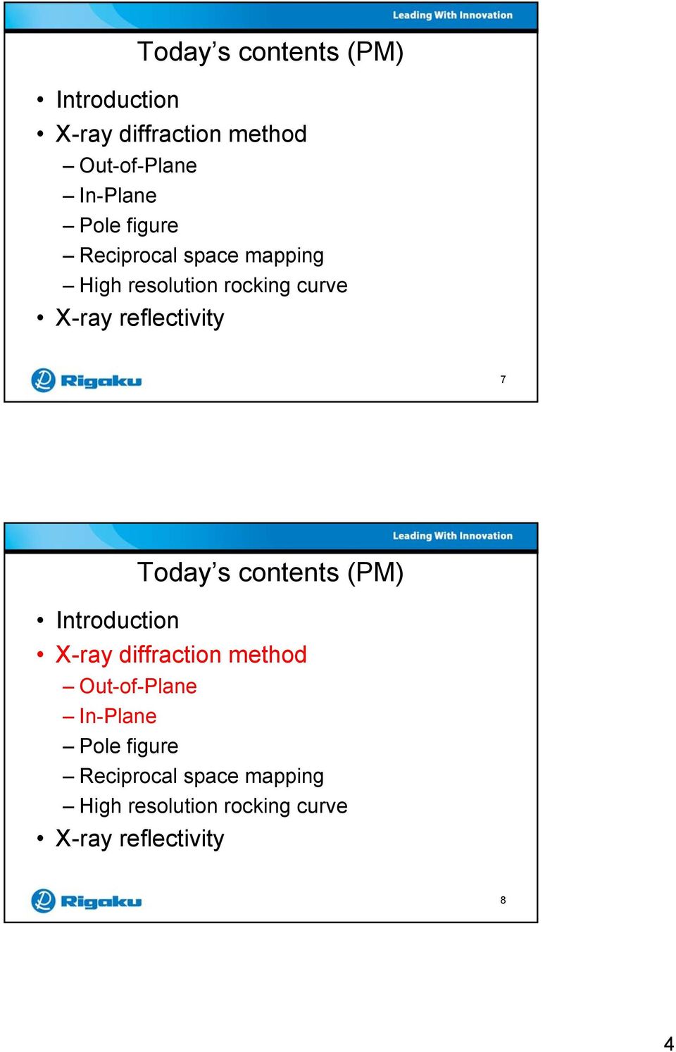
1 X-ray diffraction techniques for thin films Rigaku Corporation Application Laboratory Takayuki Konya 1 Today s contents (PM) Introduction X-ray diffraction method Out-of-Plane In-Plane Pole figure Reciprocal space mapping High resolution rocking curve X-ray reflectivity 2 1

2 Advantage of X-ray diffraction (XRD) method Probed depth control by incidence angle Nondestructive Measurement under atmosphere pressure 3 What can we see? a,b,c Thickness, Density, Roughness Phase Identification Interface, transition layer, etc Crystal structure Crystal quality, lattice parameter, etc Crystal orientation Single: orientation relation of substrate & film Poly: preferred orientation? (hkl) ρ, σ d 4 2

3 What XRD reveals Position and coordinate of reciprocal lattice points lattice constant crystal orientation lattice distortion K spread of reciprocal lattice points degree of preferred orientation Shape of a reciprocal lattice distribution crystal perfection defects mosaicity 5 Structure parameters Structure Parameter Order Analysis Method Thickness 1~10 3 nm Precision :~several % Xray Reflectivity Density H 2 O~Heavy Metals Xray Reflectivity Roughness 0.2~several nm Xray Reflectivity Phase ID - In-Plane XRD Out-of-Plane XRD etc Crystal System - In-Plane XRD Out-of-Plane XRD etc Lattice Constant ~several nm Precision : 0.05~ nm In-Plane XRD Out-of-Plane XRD etc Crystal quality Poly~Single, Perfect In-Plane XRD Crystals Out-of-Plane XRD etc Preferred Random~Preferred Orientation Orientation ~Single Crystal Pole Figure ect Orientation Relation Relation between Film & Substrate Rocking Curve Reciprocal Space Map etc Layer Structure Crystal Structure 6 3

4 Today s contents (PM) Introduction X-ray diffraction method Out-of-Plane In-Plane Pole figure Reciprocal space mapping High resolution rocking curve X-ray reflectivity 7 Today s contents (PM) Introduction X-ray diffraction method Out-of-Plane In-Plane Pole figure Reciprocal space mapping High resolution rocking curve X-ray reflectivity 8 4
5 Difference between Scan Modes The orientation of observed crystal plane depends on scanning mode. Out-of-Plane scan Film scan In-Plane scan Observed plane is.. Observed plane is.. parallel to the surface tilting (changing during a scan) perpendicular to the surface 9 What is In-Plane XRD? The detector moves parallel to the surface. Incident x-ray Diffracted x-ray α Diffraction angle 2θ B Reflected x-ray Grazing incidence (fixed angle) Observing planes are perpendicular to the surface. 10 5
 perpendicular to the surface 9 What is In-Plane XRD?")
6 Outward of In-Plane Attachment Scanning motion is completely perpendicular to θ/2θ scan. θ/2θ scan In-Plane measurement (2θχ/φ scan) 11 In-plane effect Intensity (cps) In Plane θχ/φ (degree) In-Plane 220 Intensity (cps) Out of Plane θ/ω (degree) Out-of-plane poly-si Glass 12 6
 70 80 90")
7 Probed depth control? 1 extinction distance (nm) incident angle (degree) Sample:Al Wavelength: Å(CuKα1) 13 Surface & Interface Structure 250 In-Plane XRD Intensity (cps) Al(111) 40 Al+Cu Al+Cu Cu(111) Cu(200) θχ/φ(degree) Incident angle 0.2 deg. 0.5 deg. Al(220) Al(311) Cu(220) Al(222) ~300nm Transition layer Al Al+Cu SiO 2 Si (substrate) Cu Ta 14 7
 Cu(200) 50 60 2θχ/φ(degree) Incident angle 0.2 deg. 0.5 deg.")
8 Today s contents (PM) Introduction Advantage of reciprocal lattice vector X-ray diffraction method Out-of-Plane In-Plane Pole figure Reciprocal space mapping High resolution rocking curve X-ray reflectivity 15 Single crystal and random orientation Single crystal Fiber orientation Random orientation 16 8

9 Orientation conditions and pole figure (111) pole figure (220) pole figure α=90 β=0 α=90 β=0 Random orientation β=90 β=270 β=90 β=270 β=180 β=180 {111} fiber orientation α=90 β=0 β=90 β=270 β=180 α=90 β=0 α=70.5 α=90 β=0 β=90 β=270 β=180 α=90 β=0 α=35.3 (111) single crystal β=90 β=270 β=90 β=270 β=180 β= Today s contents (PM) Introduction Advantage of reciprocal lattice vector X-ray diffraction method Out-of-Plane In-Plane Pole figure Reciprocal space mapping High resolution rocking curve X-ray reflectivity 18 9

10 Reciprocal space mapping Diffraction intensity distribution is plotted on reciprocal space. 2θ/ω g hkl Δω k g 2θ/ω k o ω 19 Epitaxial layer structures Relaxation Strain Misorientation 00l cubic[112] 00l substrate[001] cubic[112] 00l film[001] tetragonal[112] hh0 hh0 hh

11 Reciprocal space mapping Mosaic spread GaAs115 q y / -1 AlGaAs115 Broadening in direction of sample rotation Mismatch (strained) q x / -1 Broadening in direction of radial scan 21 Today s contents (PM) Introduction Advantage of reciprocal lattice vector X-ray diffraction method Out-of-Plane In-Plane Pole figure Reciprocal space mapping High resolution rocking curve X-ray reflectivity 22 11

12 High- resolution rocking curve The differences of lattice spacing between the substrate and epitaxial films are observed. Thickness and composition ratio of epitaxial films (when the degree of relaxation is known. ) 2θ/ω K ghkl k g log(i ) k o Δ2θ/ω 23 When the sample has multilayer structure Complicated oscillation composed of oscillation from each layer is observed. Reflectivity GeSi GeSi Si (004) Ge x Si (1-x) 50nm Ge x Si (1-x) 300nm x=0.015 Si substrate Deviation Angle (arcseconds) x=0.050 x=
 Ge x Si (1-x) 50nm Ge x Si (1-x) 300nm x=0.")
13 When the sample has superlattice structure Satellite peaks are observed GaAs (004) Reflectivity GaAs 5nm In x Ga (1-x) As 5nm GaAs substrate 10L Deviation Angle (arcseconds) x= How to interpret the profile Si substrate (004) SiGe mismatch Reflectivity Intensity SiGe mismatch 10-3 Oscillation period SiGe thickness 10-5 Ge x Si (1-x) 50nm x=0.050 Ge x Si (1-x) 300nm x=0.015 Si substrate Oscillation period 2SiGe thickness diffraction Deviation Angle angle (arcseconds) (Δarcsec.) 26 13
 10-1 2SiGe mismatch Reflectivity Intensity 10-2 1SiGe mismatch 10-3 Oscillation period 10-4 1SiGe")
14 Today s contents (PM) Introduction X-ray diffraction method Out-of-Plane In-Plane Pole figure Reciprocal space mapping High resolution rocking curve X-ray reflectivity 27 What reflectivity reveals X-ray reflectivity nondestructively reveals - layer structure of multi layers - thickness (1 to 1000nm) - density as an absolute value - surface and interface roughness Interface roughness thickness layer 1 thickness layer 2 density substrate 28 14

15 How to interpret the profile Critical angle c Density Reflectivity Amplitude of 10-4 oscillation Contrast 10-5 of density 0 2 Period of oscillation Thickness 4 2θ/θ (degree) roughness 1 roughness 2 roughness 3 Decay of amplitude Interface roughness 6 8 density 1 density 2 density 3 layer 1 layer 2 substrate Decay of reflectivity Surface roughness thickness 1 thickness 2 29 X-ray reflectivity measurement of TiN film 10 0 TiN SiO 2 Si Reflectivity Simulation Experimental Layer density (g/cm 3 ) Thickness (nm) Roughness (nm) TiN TiN SiO Si substrate Grancing angle α (degree) 1.5 Coating layer
 Thickness (nm) Roughness (nm) TiN 3.680 1.230 1.420 TiN 2.900 8.400 1.000 SiO 2 2.260 127.700 0.220 Si substrate 0.0 0.5 1.0 Grancing angle α (degree) 1.")
X-ray thin-film measurement techniques
 Technical articles X-ray thin-film measurement techniques II. Out-of-plane diffraction measurements Toru Mitsunaga* 1. Introduction A thin-film sample is two-dimensionally formed on the surface of a substrate,
X-Ray Diffraction HOW IT WORKS WHAT IT CAN AND WHAT IT CANNOT TELL US. Hanno zur Loye
 X-Ray Diffraction HOW IT WORKS WHAT IT CAN AND WHAT IT CANNOT TELL US Hanno zur Loye X-rays are electromagnetic radiation of wavelength about 1 Å (10-10 m), which is about the same size as an atom. The
Introduction to X-Ray Powder Diffraction Data Analysis
 Introduction to X-Ray Powder Diffraction Data Analysis Center for Materials Science and Engineering at MIT http://prism.mit.edu/xray An X-ray diffraction pattern is a plot of the intensity of X-rays scattered
Spectroscopic Ellipsometry:
 Spectroscopic : What it is, what it will do, and what it won t do by Harland G. Tompkins Introduction Fundamentals Anatomy of an ellipsometric spectrum Analysis of an ellipsometric spectrum What you can
Chapter 8. Low energy ion scattering study of Fe 4 N on Cu(100)
") Low energy ion scattering study of 4 on Cu(1) Chapter 8. Low energy ion scattering study of 4 on Cu(1) 8.1. Introduction For a better understanding of the reconstructed 4 surfaces one would like to know
Low energy ion scattering study of 4 on Cu(1) Chapter 8. Low energy ion scattering study of 4 on Cu(1) 8.1. Introduction For a better understanding of the reconstructed 4 surfaces one would like to know
High-Resolution X-ray Diffraction of Epitaxial Thin-Films and Patterned Nanostructures. Matthew Wormington
 High-Resolution X-ray Diffraction of Epitaxial Thin-Films and Patterned Nanostructures Matthew Wormington Acknowledgements Colleagues Paul Ryan & John Wall (JV UK) Kevin Matney & Peter Gin (JV US) Isaac
X-ray Diffraction and EBSD
 X-ray Diffraction and EBSD Jonathan Cowen Swagelok Center for the Surface Analysis of Materials Case School of Engineering Case Western Reserve University October 27, 2014 Outline X-ray Diffraction (XRD)
Glancing XRD and XRF for the Study of Texture Development in SmCo Based Films Sputtered Onto Silicon Substrates
 161 162 Glancing XRD and XRF for the Study of Texture Development in SmCo Based Films Sputtered Onto Silicon Substrates F. J. Cadieu*, I. Vander, Y. Rong, and R. W. Zuneska Physics Department Queens College
Crystal Structure Determination I
 Crystal Structure Determination I Dr. Falak Sher Pakistan Institute of Engineering and Applied Sciences National Workshop on Crystal Structure Determination using Powder XRD, organized by the Khwarzimic
Applications of New, High Intensity X-Ray Optics - Normal and thin film diffraction using a parabolic, multilayer mirror
 Applications of New, High Intensity X-Ray Optics - Normal and thin film diffraction using a parabolic, multilayer mirror Stephen B. Robie scintag, Inc. 10040 Bubb Road Cupertino, CA 95014 Abstract Corundum
DIEGO TONINI MORPHOLOGY OF NIOBIUM FILMS SPUTTERED AT DIFFERENT TARGET SUBSTRATE ANGLE
 UNIVERSITÀ DEGLI STUDI DI PADOVA SCIENCE FACULTY MATERIAL SCIENCE DEGREE INFN LABORATORI NAZIONALI DI LEGNARO DIEGO TONINI MORPHOLOGY OF NIOBIUM FILMS SPUTTERED AT DIFFERENT TARGET SUBSTRATE ANGLE 2 QUESTIONS
Sputtered AlN Thin Films on Si and Electrodes for MEMS Resonators: Relationship Between Surface Quality Microstructure and Film Properties
 Sputtered AlN Thin Films on and Electrodes for MEMS Resonators: Relationship Between Surface Quality Microstructure and Film Properties S. Mishin, D. R. Marx and B. Sylvia, Advanced Modular Sputtering,
Types of Epitaxy. Homoepitaxy. Heteroepitaxy
 Epitaxy Epitaxial Growth Epitaxy means the growth of a single crystal film on top of a crystalline substrate. For most thin film applications (hard and soft coatings, optical coatings, protective coatings)
Structure Factors 59-553 78
 78 Structure Factors Until now, we have only typically considered reflections arising from planes in a hypothetical lattice containing one atom in the asymmetric unit. In practice we will generally deal
Laue lens for Nuclear Medicine
 Laue lens for Nuclear Medicine PhD in Physics Gianfranco Paternò Ferrara, 6-11-013 Supervisor: prof. Vincenzo Guidi Sensors and Semiconductors Lab, Department of Physics and Earth Science, University of
Optical Properties of Sputtered Tantalum Nitride Films Determined by Spectroscopic Ellipsometry
 Optical Properties of Sputtered Tantalum Nitride Films Determined by Spectroscopic Ellipsometry Thomas Waechtler a, Bernd Gruska b, Sven Zimmermann a, Stefan E. Schulz a, Thomas Gessner a a Chemnitz University
ORIENTATION CHARACTERISTICS OF THE MICROSTRUCTURE OF MATERIALS
 ORIENTATION CHARACTERISTICS OF THE MICROSTRUCTURE OF MATERIALS K. Sztwiertnia Polish Academy of Sciences, Institute of Metallurgy and Materials Science, 25 Reymonta St., 30-059 Krakow, Poland MMN 2009
6) How wide must a narrow slit be if the first diffraction minimum occurs at ±12 with laser light of 633 nm?
 How wide must a narrow slit be if the first diffraction minimum occurs at ±12 with laser light of 633 nm?") Test IV Name 1) In a single slit diffraction experiment, the width of the slit is 3.1 10-5 m and the distance from the slit to the screen is 2.2 m. If the beam of light of wavelength 600 nm passes through
Test IV Name 1) In a single slit diffraction experiment, the width of the slit is 3.1 10-5 m and the distance from the slit to the screen is 2.2 m. If the beam of light of wavelength 600 nm passes through
USING MATLAB FOR MATERIALS DESIGN: DESCRIBING GRAIN ORIENTATIONS IN METALS Claes Olsson, PhD - Docent / Sandvik Materials Technology
 USING MATLAB FOR MATERIALS DESIGN: DESCRIBING GRAIN ORIENTATIONS IN METALS Claes Olsson, PhD - Docent / Sandvik Materials Technology THE SANDVIK GROUP MACHINING SOLUTIONS MINING AND CONSTRUCTION MATERIALS
X-Ray Study of Soft and Hard Magnetic Thin Films
 Copyright (C) JCPDS-International Centre for Diffraction Data 1999 13 X-Ray Study of Soft and Hard Magnetic Thin Films Po-Wen Wang, 390 Reed St., Stormedia, Inc., Santa Clara CA. 95050 Abstract : This
X-ray Diffraction (XRD)
") X-ray Diffraction (XRD) 1.0 What is X-ray Diffraction 2.0 Basics of Crystallography 3.0 Production of X-rays 4.0 Applications of XRD 5.0 Instrumental Sources of Error 6.0 Conclusions Bragg s Law n l =2dsinq
X-ray Diffraction (XRD) 1.0 What is X-ray Diffraction 2.0 Basics of Crystallography 3.0 Production of X-rays 4.0 Applications of XRD 5.0 Instrumental Sources of Error 6.0 Conclusions Bragg s Law n l =2dsinq
X-ray analysis methods
 2008 Advanced Materials Characterization Workshop X-ray analysis methods Mauro Sardela, Ph.D. The Frederick Seitz Materials Research Laboratory University of Illinois at Urbana-Champaign Sponsors: Sponsors:
STRUCTURAL STUDIES OF MULTIFERROIC THIN FILMS
 STRUCTURAL STUDIES OF MULTIFERROIC THIN FILMS Lisa Krayer (UCSD) Mentor: Daniel Pajerowski (NIST) Collaborating with: (University of Florida) Professor Amlan Biswas Daniel Grant NCNR
Physics 441/2: Transmission Electron Microscope
 Physics 441/2: Transmission Electron Microscope Introduction In this experiment we will explore the use of transmission electron microscopy (TEM) to take us into the world of ultrasmall structures. This
Crystal Structure of High Temperature Superconductors. Marie Nelson East Orange Campus High School NJIT Professor: Trevor Tyson
 Crystal Structure of High Temperature Superconductors Marie Nelson East Orange Campus High School NJIT Professor: Trevor Tyson Introduction History of Superconductors Superconductors are material which
Scanning Near Field Optical Microscopy: Principle, Instrumentation and Applications
 Scanning Near Field Optical Microscopy: Principle, Instrumentation and Applications Saulius Marcinkevičius Optics, ICT, KTH 1 Outline Optical near field. Principle of scanning near field optical microscope
Microscopy and Nanoindentation. Combining Orientation Imaging. to investigate localized. deformation behaviour. Felix Reinauer
 Combining Orientation Imaging Microscopy and Nanoindentation to investigate localized deformation behaviour Felix Reinauer René de Kloe Matt Nowell Introduction Anisotropy in crystalline materials Presentation
ESRF Upgrade Phase II: le nuove opportunitá per le linee da magnete curvante
 LUCI DI SINCROTRONE CNR, ROMA 22 APRILE 2014 ESRF Upgrade Phase II: le nuove opportunitá per le linee da magnete curvante Sakura Pascarelli [email protected] Page 2 INCREASE IN BRILLIANCE H emittance V emittance
Secondary Ion Mass Spectrometry
 Secondary Ion Mass Spectrometry A PRACTICAL HANDBOOK FOR DEPTH PROFILING AND BULK IMPURITY ANALYSIS R. G. Wilson Hughes Research Laboratories Malibu, California F. A. Stevie AT&T Bell Laboratories Allentown,
Coating Thickness and Composition Analysis by Micro-EDXRF
 Application Note: XRF Coating Thickness and Composition Analysis by Micro-EDXRF www.edax.com Coating Thickness and Composition Analysis by Micro-EDXRF Introduction: The use of coatings in the modern manufacturing
EXPERIMENTAL STUDY OF STRUCTURAL ZONE MODEL FOR COMPOSITE THIN FILMS IN MAGNETIC RECORDING MEDIA APPLICATION
 EXPERIMENTAL STUDY OF STRUCTURAL ZONE MODEL FOR COMPOSITE THIN FILMS IN MAGNETIC RECORDING MEDIA APPLICATION Hua Yuan and David E. Laughlin Department of Materials Science and Engineering, Carnegie Mellon
Electron density is complex!
 Electron density is complex! Göttingen, November 13 th 2008 George M. Sheldrick, Göttingen University http://shelx.uni-ac.gwdg.de/shelx/ Friedel s Law F h,k,l = F h, k, l and φ h,k,l = φ h, k, l Friedel
Applications of Infrared Multiple Angle Incidence Resolution Spectrometry
 Electronically reprinted from August 2015 Applications of Infrared Multiple Angle Incidence Resolution Spectrometry Multiple angle incidence resolution spectrometry (MAIRS has proven useful for characterization
Chapter 3. 1. 3 types of materials- amorphous, crystalline, and polycrystalline. 5. Same as #3 for the ceramic and diamond crystal structures.
 Chapter Highlights: Notes: 1. types of materials- amorphous, crystalline, and polycrystalline.. Understand the meaning of crystallinity, which refers to a regular lattice based on a repeating unit cell..
Raman spectroscopy Lecture
 Raman spectroscopy Lecture Licentiate course in measurement science and technology Spring 2008 10.04.2008 Antti Kivioja Contents - Introduction - What is Raman spectroscopy? - The theory of Raman spectroscopy
NEAR FIELD OPTICAL MICROSCOPY AND SPECTROSCOPY WITH STM AND AFM PROBES
 Vol. 93 (1997) A CTA PHYSICA POLONICA A No. 2 Proceedings of the 1st International Symposium on Scanning Probe Spectroscopy and Related Methods, Poznań 1997 NEAR FIELD OPTICAL MICROSCOPY AND SPECTROSCOPY
- particle with kinetic energy E strikes a barrier with height U 0 > E and width L. - classically the particle cannot overcome the barrier
 Tunnel Effect: - particle with kinetic energy E strikes a barrier with height U 0 > E and width L - classically the particle cannot overcome the barrier - quantum mechanically the particle can penetrated
Magnetic Field of a Circular Coil Lab 12
 HB 11-26-07 Magnetic Field of a Circular Coil Lab 12 1 Magnetic Field of a Circular Coil Lab 12 Equipment- coil apparatus, BK Precision 2120B oscilloscope, Fluke multimeter, Wavetek FG3C function generator,
WAVELENGTH OF LIGHT - DIFFRACTION GRATING
 PURPOSE In this experiment we will use the diffraction grating and the spectrometer to measure wavelengths in the mercury spectrum. THEORY A diffraction grating is essentially a series of parallel equidistant
Chapter 7: Basics of X-ray Diffraction
 Providing Solutions To Your Diffraction Needs. Chapter 7: Basics of X-ray Diffraction Scintag has prepared this section for use by customers and authorized personnel. The information contained herein is
Nanometer-scale imaging and metrology, nano-fabrication with the Orion Helium Ion Microscope
 [email protected] Nanometer-scale imaging and metrology, nano-fabrication with the Orion Helium Ion Microscope Bin Ming, András E. Vladár and Michael T. Postek National Institute of Standards and Technology
Defects Introduction. Bonding + Structure + Defects. Properties
 Defects Introduction Bonding + Structure + Defects Properties The processing determines the defects Composition Bonding type Structure of Crystalline Processing factors Defects Microstructure Types of
Development of Optical Wave Microphone Measuring Sound Waves with No Diaphragm
 Progress In Electromagnetics Research Symposium Proceedings, Taipei, March 5 8, 3 359 Development of Optical Wave Microphone Measuring Sound Waves with No Diaphragm Yoshito Sonoda, Takashi Samatsu, and
NPL REPORT DEPC-MPR 014
 NPL REPORT DEPC-MPR 014 Developing a Test Method to Characterise Internal Stress in Tin Coatings: Phase 2 Martin Wickham, Tony Fry, Dipak Gohil and Chris Hunt NOT RESTRICTED JANUARY 2005 National Physical
COMPARISON OF TEXTURE IN COPPER AND ALUMINUM THIN FILMS DETERMINED BY XRD AND EBSD *
 201 COMPARISON OF TEXTURE IN COPPER AND ALUMINUM THIN FILMS DETERMINED BY XRD AND EBSD * J. Müller 1, D. Balzar 1,2, R.H. Geiss 1, D.T. Read 1, and R.R. Keller 1 1 Materials Reliability Division, National
Crystal Optics of Visible Light
 Crystal Optics of Visible Light This can be a very helpful aspect of minerals in understanding the petrographic history of a rock. The manner by which light is transferred through a mineral is a means
Nanoelectronics 09. Atsufumi Hirohata Department of Electronics. Quick Review over the Last Lecture
 Nanoelectronics 09 Atsufumi Hirohata Department of Electronics 12:00 Wednesday, 4/February/2015 (P/L 006) Quick Review over the Last Lecture ( Field effect transistor (FET) ): ( Drain ) current increases
Preparation of ZnS and SnS Nanopowders by Modified SILAR Technique
 Journal of Physical Sciences, Vol. 13, 009, 9-34 ISSN: 097-8791 : www.vidyasagar.ac.in/journal Preparation of ZnS and SnS Nanopowders by Modified SILAR Technique Department of Physics The University of
Supplementary Material (ESI) for Chemical Communications This journal is (c) The Royal Society of Chemistry 2009
 for Chemical Communications This journal is (c) The Royal Society of Chemistry 2009") Supporting Information Supplementary Material (ESI) for Chemical Communications Controlled Synthesis of Co 3 O 4 Nanopolyhedrons and Nanosheets at Low Temperature Hongying Liang a, Joan M. Raitano a, Lihua
Supporting Information Supplementary Material (ESI) for Chemical Communications Controlled Synthesis of Co 3 O 4 Nanopolyhedrons and Nanosheets at Low Temperature Hongying Liang a, Joan M. Raitano a, Lihua
Plate waves in phononic crystals slabs
 Acoustics 8 Paris Plate waves in phononic crystals slabs J.-J. Chen and B. Bonello CNRS and Paris VI University, INSP - 14 rue de Lourmel, 7515 Paris, France [email protected] 41 Acoustics 8 Paris We
Experiment: Crystal Structure Analysis in Engineering Materials
 Experiment: Crystal Structure Analysis in Engineering Materials Objective The purpose of this experiment is to introduce students to the use of X-ray diffraction techniques for investigating various types
Introduction to Powder X-Ray Diffraction History Basic Principles
 Introduction to Powder X-Ray Diffraction History Basic Principles Folie.1 History: Wilhelm Conrad Röntgen Wilhelm Conrad Röntgen discovered 1895 the X-rays. 1901 he was honoured by the Noble prize for
This is an author-deposited version published in: http://sam.ensam.eu Handle ID:.http://hdl.handle.net/10985/10324
 Science Arts & Métiers (SAM) is an open access repository that collects the work of Arts et Métiers ParisTech researchers and makes it freely available over the web where possible. This is an author-deposited
Determination of source parameters from seismic spectra
 Topic Determination of source parameters from seismic spectra Authors Michael Baumbach, and Peter Bormann (formerly GeoForschungsZentrum Potsdam, Telegrafenberg, D-14473 Potsdam, Germany); E-mail: [email protected]
Fundamentals of grain boundaries and grain boundary migration
 1. Fundamentals of grain boundaries and grain boundary migration 1.1. Introduction The properties of crystalline metallic materials are determined by their deviation from a perfect crystal lattice, which
Rigaku XRD-System Instruction Manual v4/19/03. The Krishnan Group/Wilcox 132, University of Washington
 Rigaku XRD-System Instruction Manual v4/19/03 The Krishnan Group/Wilcox 132, University of Washington Contents: - General information - Safety - How to turn on the X-rays - How to turn off the X-rays -
POWDER X-RAY DIFFRACTION: STRUCTURAL DETERMINATION OF ALKALI HALIDE SALTS
 EXPERIMENT 4 POWDER X-RAY DIFFRACTION: STRUCTURAL DETERMINATION OF ALKALI HALIDE SALTS I. Introduction The determination of the chemical structure of molecules is indispensable to chemists in their effort
Theremino System Theremino Spectrometer Technology
 Theremino System Theremino Spectrometer Technology theremino System - Theremino Spectrometer Technology - August 15, 2014 - Page 1 Operation principles By placing a digital camera with a diffraction grating
X-ray diffraction in polymer science
 X-ray diffraction in polymer science 1) Identification of semicrystalline polymers and Recognition of crystalline phases (polymorphism) of polymers 2)Polymers are never 100% crystalline. XRD is a primary
Ajit Kumar Patra (Autor) Crystal structure, anisotropy and spin reorientation transition of highly coercive, epitaxial Pr-Co films
 Crystal structure, anisotropy and spin reorientation transition of highly coercive, epitaxial Pr-Co films") Ajit Kumar Patra (Autor) Crystal structure, anisotropy and spin reorientation transition of highly coercive, epitaxial Pr-Co films https://cuvillier.de/de/shop/publications/1306 Copyright: Cuvillier Verlag,
Ajit Kumar Patra (Autor) Crystal structure, anisotropy and spin reorientation transition of highly coercive, epitaxial Pr-Co films https://cuvillier.de/de/shop/publications/1306 Copyright: Cuvillier Verlag,
Plastic Film Texture Measurement With 3D Profilometry
 Plastic Film Texture Measurement With 3D Profilometry Prepared by Jorge Ramirez 6 Morgan, Ste156, Irvine CA 92618 P: 949.461.9292 F: 949.461.9232 nanovea.com Today's standard for tomorrow's materials.
Ultrasonic Wave Propagation Review
 Ultrasonic Wave Propagation Review Presented by: Sami El-Ali 1 1. Introduction Ultrasonic refers to any study or application of sound waves that are higher frequency than the human audible range. Ultrasonic
Solid State Theory Physics 545
 Solid State Theory Physics 545 CRYSTAL STRUCTURES Describing periodic structures Terminology Basic Structures Symmetry Operations Ionic crystals often have a definite habit which gives rise to particular
Micro-Power Generation
 Micro-Power Generation Elizabeth K. Reilly February 21, 2007 TAC-meeting 1 Energy Scavenging for Wireless Sensors Enabling Wireless Sensor Networks: Ambient energy source Piezoelectric transducer technology
Solid State Detectors = Semi-Conductor based Detectors
 Solid State Detectors = Semi-Conductor based Detectors Materials and their properties Energy bands and electronic structure Charge transport and conductivity Boundaries: the p-n junction Charge collection
Martensite in Steels
 Materials Science & Metallurgy http://www.msm.cam.ac.uk/phase-trans/2002/martensite.html H. K. D. H. Bhadeshia Martensite in Steels The name martensite is after the German scientist Martens. It was used
5. Scanning Near-Field Optical Microscopy 5.1. Resolution of conventional optical microscopy
 5. Scanning Near-Field Optical Microscopy 5.1. Resolution of conventional optical microscopy Resolution of optical microscope is limited by diffraction. Light going through an aperture makes diffraction
Chapter Outline Dislocations and Strengthening Mechanisms
 Chapter Outline Dislocations and Strengthening Mechanisms What is happening in material during plastic deformation? Dislocations and Plastic Deformation Motion of dislocations in response to stress Slip
COMPARISON OF FOUR DATA ANALYSIS SOFTWARE FOR COMBINED X-RAY REFLECTIVITY AND GRAZING INCIDENCE X-RAY FLUORESCENCE MEASUREMENTS
 COMPARISON OF FOUR DATA ANALYSIS SOFTWARE FOR COMBINED X-RAY REFLECTIVITY AND GRAZING INCIDENCE X-RAY FLUORESCENCE MEASUREMENTS Bérenger Caby (1), Fabio Brigidi (2), Dieter Ingerle (3), Blanka Detlefs
Lecture 12. Physical Vapor Deposition: Evaporation and Sputtering Reading: Chapter 12. ECE 6450 - Dr. Alan Doolittle
 Lecture 12 Physical Vapor Deposition: Evaporation and Sputtering Reading: Chapter 12 Evaporation and Sputtering (Metalization) Evaporation For all devices, there is a need to go from semiconductor to metal.
SPM 150 Aarhus with KolibriSensor
 Customied Systems and Solutions Nanostructures and Thin Film Deposition Surface Analysis and Preparation Components Surface Science Applications SPM 150 Aarhus with KolibriSensor Atomic resolution NC-AFM
Chapter 3: Structure of Metals and Ceramics. Chapter 3: Structure of Metals and Ceramics. Learning Objective
 Chapter 3: Structure of Metals and Ceramics Chapter 3: Structure of Metals and Ceramics Goals Define basic terms and give examples of each: Lattice Basis Atoms (Decorations or Motifs) Crystal Structure
Chapter Outline. How do atoms arrange themselves to form solids?
 Chapter Outline How do atoms arrange themselves to form solids? Fundamental concepts and language Unit cells Crystal structures Simple cubic Face-centered cubic Body-centered cubic Hexagonal close-packed
Structural Integrity Analysis
 Structural Integrity Analysis 1. STRESS CONCENTRATION Igor Kokcharov 1.1 STRESSES AND CONCENTRATORS 1.1.1 Stress An applied external force F causes inner forces in the carrying structure. Inner forces
SURFACE TENSION. Definition
 SURFACE TENSION Definition In the fall a fisherman s boat is often surrounded by fallen leaves that are lying on the water. The boat floats, because it is partially immersed in the water and the resulting
Chapter Outline Dislocations and Strengthening Mechanisms
 Chapter Outline Dislocations and Strengthening Mechanisms What is happening in material during plastic deformation? Dislocations and Plastic Deformation Motion of dislocations in response to stress Slip
Ionosphere Properties and Behaviors - Part 2 By Marcel H. De Canck, ON5AU
 Ionosphere Properties and Behaviors - Part 2 By Marcel H. De Canck, ON5AU I n the previous issue I explained that gyrofrequency depends on the earth s magnetic field and mentioned that this magnetic field
3D TOPOGRAPHY & IMAGE OVERLAY OF PRINTED CIRCUIT BOARD ASSEMBLY
 3D TOPOGRAPHY & IMAGE OVERLAY OF PRINTED CIRCUIT BOARD ASSEMBLY Prepared by Duanjie Li, PhD & Andrea Novitsky 6 Morgan, Ste156, Irvine CA 92618 P: 949.461.9292 F: 949.461.9232 nanovea.com Today's standard
Using light scattering method to find The surface tension of water
 Experiment (8) Using light scattering method to find The surface tension of water The aim of work: The goals of this experiment are to confirm the relationship between angular frequency and wave vector
Basic Properties and Application Examples of PGS Graphite Sheet
 Basic Properties and Application Examples of 1. Basic properties of Graphite sheet 2. Functions of Graphite sheet 3. Application Examples Presentation [Sales Liaison] Panasonic Electronic Devices Co.,
X-RAY DIFFRACTION IMAGING AS A TOOL OF MESOSTRUCTURE ANALYSIS
 Copyright(c)JCPDS-International Centre for Diffraction Data 2001,Advances in X-ray Analysis,Vol.44 241 X-RAY DIFFRACTION IMAGING AS A TOOL OF MESOSTRUCTURE ANALYSIS ABSTRACT J. Fiala, S. Němeček Škoda
LECTURE SUMMARY September 30th 2009
 LECTURE SUMMARY September 30 th 2009 Key Lecture Topics Crystal Structures in Relation to Slip Systems Resolved Shear Stress Using a Stereographic Projection to Determine the Active Slip System Slip Planes
DOE Solar Energy Technologies Program Peer Review. Denver, Colorado April 17-19, 2007
 DOE Solar Energy Technologies Program Peer Review Evaluation of Nanocrystalline Silicon Thin Film by Near-Field Scanning Optical Microscopy AAT-2-31605-05 Magnus Wagener and George Rozgonyi North Carolina
Polarization of Light
 Polarization of Light References Halliday/Resnick/Walker Fundamentals of Physics, Chapter 33, 7 th ed. Wiley 005 PASCO EX997A and EX999 guide sheets (written by Ann Hanks) weight Exercises and weights
rotation,, axis of rotoinversion,, center of symmetry, and mirror planes can be
 Crystal Symmetry The external shape of a crystal reflects the presence or absence of translation-free symmetry y elements in its unit cell. While not always immediately obvious, in most well formed crystal
Electron Microscopy 3. SEM. Image formation, detection, resolution, signal to noise ratio, interaction volume, contrasts
 Electron Microscopy 3. SEM Image formation, detection, resolution, signal to noise ratio, interaction volume, contrasts 3-1 SEM is easy! Just focus and shoot "Photo"!!! Please comment this picture... Any
Manual for simulation of EB processing. Software ModeRTL
 1 Manual for simulation of EB processing Software ModeRTL How to get results. Software ModeRTL. Software ModeRTL consists of five thematic modules and service blocks. (See Fig.1). Analytic module is intended
h e l p s y o u C O N T R O L
 contamination analysis for compound semiconductors ANALYTICAL SERVICES B u r i e d d e f e c t s, E v a n s A n a l y t i c a l g r o u p h e l p s y o u C O N T R O L C O N T A M I N A T I O N Contamination
" {h k l } lop x odl. ORxOS. (2) Determine the interplanar angle between these two planes:
 Determine the interplanar angle between these two planes:") Textures and Microstructures, 1991, Vols 14-18, pp. 273-278 Reprints available from the publisher Photocopying permitted by license only (C) 1991 Gordon and Breach Science Publishers SA Printed in the
Textures and Microstructures, 1991, Vols 14-18, pp. 273-278 Reprints available from the publisher Photocopying permitted by license only (C) 1991 Gordon and Breach Science Publishers SA Printed in the
CREOL, College of Optics & Photonics, University of Central Florida
 OSE6650 - Optical Properties of Nanostructured Materials Optical Properties of Nanostructured Materials Fall 2013 Class 3 slide 1 Challenge: excite and detect the near field Thus far: Nanostructured materials
Near-field scanning optical microscopy (SNOM)
") Adviser: dr. Maja Remškar Institut Jožef Stefan January 2010 1 2 3 4 5 6 Fluorescence Raman and surface enhanced Raman 7 Conventional optical microscopy-limited resolution Two broad classes of techniques
Adviser: dr. Maja Remškar Institut Jožef Stefan January 2010 1 2 3 4 5 6 Fluorescence Raman and surface enhanced Raman 7 Conventional optical microscopy-limited resolution Two broad classes of techniques
Powder diffraction and synchrotron radiation
 Powder diffraction and synchrotron radiation Gilberto Artioli Dip. Geoscienze UNIPD CIRCe Center for Cement Materials single xl diffraction powder diffraction Ideal powder Powder averaging Textured sample
Optical Communications
 Optical Communications Telecommunication Engineering School of Engineering University of Rome La Sapienza Rome, Italy 2005-2006 Lecture #2, May 2 2006 The Optical Communication System BLOCK DIAGRAM OF
E190Q Lecture 5 Autonomous Robot Navigation
 E190Q Lecture 5 Autonomous Robot Navigation Instructor: Chris Clark Semester: Spring 2014 1 Figures courtesy of Siegwart & Nourbakhsh Control Structures Planning Based Control Prior Knowledge Operator
P R E A M B L E. Facilitated workshop problems for class discussion (1.5 hours)
") INSURANCE SCAM OPTICS - LABORATORY INVESTIGATION P R E A M B L E The original form of the problem is an Experimental Group Research Project, undertaken by students organised into small groups working as
INSURANCE SCAM OPTICS - LABORATORY INVESTIGATION P R E A M B L E The original form of the problem is an Experimental Group Research Project, undertaken by students organised into small groups working as
Relevant Reading for this Lecture... Pages 83-87.
 LECTURE #06 Chapter 3: X-ray Diffraction and Crystal Structure Determination Learning Objectives To describe crystals in terms of the stacking of planes. How to use a dot product to solve for the angles
Preface Light Microscopy X-ray Diffraction Methods
 Preface xi 1 Light Microscopy 1 1.1 Optical Principles 1 1.1.1 Image Formation 1 1.1.2 Resolution 3 1.1.3 Depth of Field 5 1.1.4 Aberrations 6 1.2 Instrumentation 8 1.2.1 Illumination System 9 1.2.2 Objective
MORPHOLOGY OF NIOBIUM FILMS SPUTTERED AT DIFFERENT TARGET SUBSTRATE ANGLE
 MORPHOLOGY OF NIOBIUM FILMS SPUTTERED AT DIFFERENT TARGET SUBSTRATE ANGLE D. Tonini *, C. Greggio, G. Keppel, F. Laviano $, M. Musiani, G. Torzo and V. Palmieri * Università degli Studi di Padova; INFN-LNL