Heterogeneous Sensor System on Chip
|
|
|
- Clinton McKinney
- 8 years ago
- Views:
Transcription
1 Introduction of M2M Networks Heterogeneous Sensor System on Chip Chih Ting Lin Yi Chang Lu Graduate Institute of Electronics Engineering National Taiwan University

2

3 Billions of Connected Devices

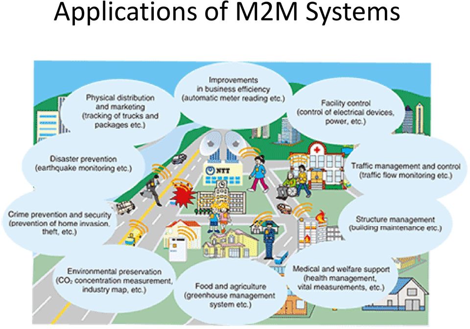
4 Applications of M2M Systems
5 Infrastructures of M2M System

6 OSI 7 Layer Network Model Open System Interconnection model A reference model developed by ISO at 1984 Layer 7: Application layer Defines interface to user processes for communication and data transfer in network Layer 6: Presentation layer Masks the differences of data formats between dissimilar systems Layer 5: Session Layer Manages user sessions and dialogues Layer 4: Transport Layer Manages end to end message delivery in network Layer 3: Network Layer Determines how data are transferred between network devices Layer 2: Data Link Layer Defines procedures for operating the communication links Layer 1: Physical Layer Defines physical means of sending data over network devices

7 M2M Network Layers

8 Sensor Networks Sensor network systems A system consisting of a collective of networked sensor nodes designed to communicate to each other Integrate sensor, micro processor, and communication capabilities Sense environment, acquire information, and handle message Limited resources Sensor 範 圍 網 路 衛 星 或 其 他 傳 輸 媒 介

9 Previous Sensor Network Applications UC Berkeley Habitant Monitoring 2002 Develop a habitat monitoring kit Monitor sensitive wildlife and habitats Engage in the non intrusive i and non disruptive method

10 Previous Sensor Network Applications UC Berkeley Firebug 2003 Install GPS system with sensor network Enable temperature monitoring with coordination Monitor wildfire in forest

11 Previous Sensor Network Applications UC Berkeley Structural Health Monitoring of the Golden Gate Bridge 2005 Measure ambient structural vibration Install 64 nodes on GGB Collect vibrations synchronously at 1kHz rate

12 Previous Sensor Network Applications Duke Univ. Observation of Ecosystem Processes Deploy dense spatial temporal sensing of environments Buildawareness of the benefits of the technology

13 Previous Sensor Network Applications NTU (Prof. 李 世 光 ) Structural Monitoring 2002 Founded by 勞 委 會 勞 工 安 全 衛 生 研 究 所 Monitor the safety of 建 築 鷹 架 Up and low limit of admission strain strain

14 Previous Sensor Network Applications NTUT (Prof. 李 仁 貴 ) Semiconductor Fab Monitoring Monitor the equipment vibration

15 Previous Sensor Network Applications NTU (Prof. 黃 寶 儀 ) BL Live: The Elevator Report know the status t of the elevators in the building Establish mid/large scale sensor network testbed for everyday use Sensor Network

16 Previous Sensor Network Applications CGU (Prof. 林 仲 志 ) 無 線 感 測 網 路 居 家 型 退 化 偵 測 設 備 之 研 發 Measure reaction force and motion balance of elders

17 Previous Sensor Network Applications NTU (Prof. 江 昭 皚 ) 東 方 果 實 蠅 生 態 監 測 與 預 警 系 統 Measure the population of flies

18 Basic Infrastructure of Sensor Node A sensor node in WSN Microprocessor Data storage Sensor RF transceiver Energy source i Microprocessor Transceiver unit unit Power Supply unit Sensor light and temperature

19 Sensor Network Design Consideration Consideration of sensor network developments Application Environment Transmission Media Scalability Sensor Network Topology Hardware Constraints t Power Consumption Fault Tolerance Sensor Costs

20 Sensor Node Design Consideration The requirement of sensor networks Robustness, effectiveness, low cost, and small size Sensing unit Passive/active sensors Power consumption Microprocessor unit Power saving Cost/performance Communication unit IEEE (low data rate wireless PAN) Power saving

21 M2M Physical Device: Smart Sensor Node Sensors bridge physical events to systems Networking concept is rarely considered in traditional sensor designs Emphasize single sensor characterization Concentrate at different kind of sensing performance Stress thenetworklatency as the complexity sensing scope increases
22 Measure the sound Microphone
23 Accelerometer Measure e the eacceleratione at
24 Gyroscope Measure the orientation
25 Pressure Sensor Measure the pressure
26 Change the light path Optical Switch
27 Turbine Engine Generate the air thrust
28 Biomolecular Detector Measure the biomarker
29 M2M Physical Device: Smart Sensor Node Smart sensor node is necessary in M2M network Promote scopes of sensors and systems Improve system performance Lower sensor manufacturing cost Increase value of sensor nodes This project aims at heterogeneous Sensor System on ChipSystem on CMOS compatible stacking technology Pseudo 3D architecture Efficient andcompact designofsmart smart sensornodenode
30 3D ICs in the 80 s A parallel image processor from Mitsubishi T. Nishimura et al., Three dimensional IC for high performanceimage signal processor processor, IEEE International Electron Device Meeting Technical Digest, pp , Dec YC Lu 2011 Graduate Institute of Electronics Engineering, National Taiwan University
31 3D ICs in the 80 s A gate array and memory chip from NEC Kunio et al., Three dimensional ICs, having four stacked active device layers, IEEE International Electron Device Meeting Technical Digest, pp , Dec YC Lu 2011 Graduate Institute of Electronics Engineering, National Taiwan University
32 Possible Applications Sensor systems Heterogeneous integration Memory-processor systems Signaling/timing Network-on-chip Topology Field-programmable-gate-arrays Redundancy YC Lu 2011 Graduate Institute of Electronics Engineering, National Taiwan University
33 3D Technology Package stacking Die/Wafer stacking Device stacking Lu, 3D technology based circuit and architecture design, Proceedingsof of International Conferenceon Communications, Circuits, and Systems, pp , July YC Lu 2011 Graduate Institute of Electronics Engineering, National Taiwan University
34 Face to back stacking Die/Wafer Stacking Koyanagi et al., Three dimensional integration technology based on wafer bonding with vertical buries interconnections, IEEE Trans. Electron Devices, Vol. 53, No. 11, November YC Lu 2011 Graduate Institute of Electronics Engineering, National Taiwan University
35 Device Stacking 6T SRAM cells Jung et al., Highly cost effective and high performance 65nm S3 (stacked single crystal Si) SRAM technology with 25 F 2, 0.16um 2 cell anddoubly doubly stacked SSTFT cell transistors for ultra high density and high speed applications, Symposium on VLSI Technology Digest of Technical Papers, pp , June, (also see IEDM 2004) YC Lu 2011 Graduate Institute of Electronics Engineering, National Taiwan University
36 Design Considerations Through-silicon-vias(TSVs) & micro-bumps (MBs) Density Operating frequency Parasitic Styles Yield Davis et al., Demystifying 3D ICs: the pros and cons of going vertical, IEEE Design & Test of Computers, vol. 22, no. 6, pp , Nov. Dec YC Lu 2011 Graduate Institute of Electronics Engineering, National Taiwan University
37 Capacitive Coupling Gu et al., Two 10Gb/s/pin low-power interconnect methods for 3D ICs, IEEE International Solid-State State Circuit Conference, pp , February, YC Lu 2011 Graduate Institute of Electronics Engineering, National Taiwan University
38 Inductive Coupling Davis et al., Demystifying 3D ICs: the pros and cons of going vertical, IEEE Design & Test of Computers, vol. 22, no. 6, pp , Nov.-Dec YC Lu 2011 Graduate Institute of Electronics Engineering, National Taiwan University
39 Design Considerations Device characteristics Thermal Flatness Stress Device options Silicon at the same node Silicon at different nodes Silicon and other materials Active and passive YC Lu 2011 Graduate Institute of Electronics Engineering, National Taiwan University
40 Design Considerations Thermal issues Timing NBTI Leakage Thermal modeling and simulation FE/FD solvers RC network Chen et al.,, Thermal modeling and device noise properties p of three dimensional SOI technology," IEEE Trans. Electron Devices,, Vol. 54, No. 4, pp , Apr YC Lu 2011 Graduate Institute of Electronics Engineering, National Taiwan University
41 Thermal Network Analogy Parameters Voltage Current Charge Resistance Capacitance Electrical Thermal Parameters V [V ] Temperature T[K] i [A] Heat Transfer Rate q[w ] Q[C] Heat Q T [J ] Thermal Resistance R E [ V / A] [ T / W ] Thermal Capacitance C E [ C / V ] R T C T [JJ / K ] C T Equations Equations Transient Steady State 2 V R C E E V ir E V t Transient 2 T Steady State R T C T t T T qr T YC Lu 2011 Graduate Institute of Electronics Engineering, National Taiwan University
42 Design Considerations Cooling techniques Better heat sink Thermal vias Microfluidic channels Micro TE coolers Mizunuma et al.,, Thermal modeling for 3D ICs with integrated microchannel cooling, IEEE/ACM Proceedings of International Conference on Computer Aided Design, Nov YC Lu 2011 Graduate Institute of Electronics Engineering, National Taiwan University
43 Design Considerations Power integrity IR drops Supply domains Timing strategies Synchronization Self-timed Signaling g strategies I/Os Level shifters YC Lu 2011 Graduate Institute of Electronics Engineering, National Taiwan University
44 Arithmetic Units Wafer stacked kdtechnology Davis et al., An 8192 point Fast Fourier Transform 3D IC case study study, IEEE Proceedings of MWCAS, pp , 441 Aug YC Lu 2011 Graduate Institute of Electronics Engineering, National Taiwan University
45 Nonvolatile SRAM Cell Device stacked kdtechnology Wang et al., Nonvolatile SRAM cell, IEEE International Electron Devices Meeting Technical Digest, Dec YC Lu 2011 Graduate Institute of Electronics Engineering, National Taiwan University
46 Flexible Electronics Sensors Someya et al., Conformable, flexible, large area areanetworks of pressure andthermalsensors with organic transistor active matrixes, PNAS, pp , Aug YC Lu 2011 Graduate Institute of Electronics Engineering, National Taiwan University
47 Heterogeneous Sensor System on Chip System on (S 2 oc) Instead of fully integration sensing device into CMOS fb fabrication at the same layer with circuits Low temperature processes stack sensing device on the CMOS circuit The advantages by harnessing synergies of different materials and processes The capability of low cost, large area fabrication, multifunctions, and local data fusion Low power consumption CMOS circuits promote functionalities of each sensor node The improvement of network communication by local DSP capabilities The self intelligent network achieved by local fusion and computation
48 Sensor on Chip on based on Inkjet printing Gas Sensor: Quasi 3D architecture Configurable sensing elements Non contact patterning for CMOS chip stacking Stacking sensing layer on the top of CMOS chip
49 Expected Advantages of Heterogeneous S 2 oc Configurable sensing functions on a chip Printing different material for different scope Lowering manufacturing cost Promoting applied value of smart sensor nodes Low power consumption design of smart sensor node Low power organic sensing material Energy efficient i architecture t Reduced manufacturing cost of sensor nodes Stacking architecture t Low cost post process for sensing elements
50 Challenges Un stability of organic materials Employing long chain polymer to enhancestability in both thermal and electrical interference Utilizing parallel process elements design to minimize the interference from circuit closed to sensing material Low selectivity of polymer sensing elements Improving by the cross calibration of multiple sensing elements Fabrication compatibility of heterogeneous nature Using ion free polymer based sensing material Taking the advantage of low temperature process of inkjet printing technology
51 Conclusions Shift the new design paradigm of sensor nodes More sensing elements More calculation capabilities Lower power consumptions Lower manufacturing cost Harness advantages heterogeneous integration Pave the way toward M2M applications
數 位 積 體 電 路 Digital Integrated Circuits
 IEE5049 - Spring 2012 數 位 積 體 電 路 Digital Integrated Circuits Course Overview Professor Wei Hwang 黃 威 教 授 Department of Electronics Engineering National Chiao Tung University hwang@mail.nctu.edu.tw Wei
DESIGN CHALLENGES OF TECHNOLOGY SCALING
 DESIGN CHALLENGES OF TECHNOLOGY SCALING IS PROCESS TECHNOLOGY MEETING THE GOALS PREDICTED BY SCALING THEORY? AN ANALYSIS OF MICROPROCESSOR PERFORMANCE, TRANSISTOR DENSITY, AND POWER TRENDS THROUGH SUCCESSIVE
Nanocomputer & Architecture
 Nanocomputer & Architecture Yingjie Wei Western Michigan University Department of Computer Science CS 603 - Dr. Elise dedonckor Febrary 4 th, 2004 Nanocomputer Architecture Contents Overview of Nanotechnology
Energy Harvesting Powered Wireless Sensor Node and Asset Tracking Solutions in Random Vibration Environments
 White Paper Energy Harvesting Powered Wireless Sensor Node and Asset Tracking Solutions in Random Vibration Environments by Anurag Kasyap, Ph.D. April 2009 Copyright 2009 AdaptivEnergy LLC. All rights
NVM memory: A Critical Design Consideration for IoT Applications
 NVM memory: A Critical Design Consideration for IoT Applications Jim Lipman Sidense Corp. Introduction The Internet of Things (IoT), sometimes called the Internet of Everything (IoE), refers to an evolving
Static-Noise-Margin Analysis of Conventional 6T SRAM Cell at 45nm Technology
 Static-Noise-Margin Analysis of Conventional 6T SRAM Cell at 45nm Technology Nahid Rahman Department of electronics and communication FET-MITS (Deemed university), Lakshmangarh, India B. P. Singh Department
International Journal of Electronics and Computer Science Engineering 1482
 International Journal of Electronics and Computer Science Engineering 1482 Available Online at www.ijecse.org ISSN- 2277-1956 Behavioral Analysis of Different ALU Architectures G.V.V.S.R.Krishna Assistant
ECE 410: VLSI Design Course Introduction
 ECE 410: VLSI Design Course Introduction Professor Andrew Mason Michigan State University Spring 2008 ECE 410, Prof. A. Mason Lecture Notes Page i.1 Age of electronics microcontrollers, DSPs, and other
Wireless Sensor Network: Challenges, Issues and Research
 ISBN 978-93-84468-20-0 Proceedings of 2015 International Conference on Future Computational Technologies (ICFCT'2015) Singapore, March 29-30, 2015, pp. 224-228 Wireless Sensor Network: Challenges, Issues
Sensor network infrastructure for intelligent building monitoring and management system
 Sensor network infrastructure for intelligent building monitoring and management system 1 R.VENKATESH, 2 K.RADHA, 3 M.GANTHIMATHI 1.B.E-CSE, Muthayammal Engineering College, Rasipuram. 2. Assistant Professor
ISSCC 2003 / SESSION 4 / CLOCK RECOVERY AND BACKPLANE TRANSCEIVERS / PAPER 4.7
 ISSCC 2003 / SESSION 4 / CLOCK RECOVERY AND BACKPLANE TRANSCEIVERS / PAPER 4.7 4.7 A 2.7 Gb/s CDMA-Interconnect Transceiver Chip Set with Multi-Level Signal Data Recovery for Re-configurable VLSI Systems
Riding silicon trends into our future
 Riding silicon trends into our future VLSI Design and Embedded Systems Conference, Bangalore, Jan 05 2015 Sunit Rikhi Vice President, Technology & Manufacturing Group General Manager, Intel Custom Foundry
IC-EMC Simulation of Electromagnetic Compatibility of Integrated Circuits
 IC-EMC Simulation of Electromagnetic Compatibility of Integrated Circuits SUMMARY CONTENTS 1. CONTEXT 2. TECHNOLOGY TRENDS 3. MOTIVATION 4. WHAT IS IC-EMC 5. SUPPORTED STANDARD 6. EXAMPLES CONTEXT - WHY
White Paper: Pervasive Power: Integrated Energy Storage for POL Delivery
 Pervasive Power: Integrated Energy Storage for POL Delivery Pervasive Power Overview This paper introduces several new concepts for micro-power electronic system design. These concepts are based on the
Curriculum for a Master s Degree in ECE with focus on Mixed Signal SOC Design
 Curriculum for a Master s Degree in ECE with focus on Mixed Signal SOC Design Department of Electrical and Computer Engineering Overview The VLSI Design program is part of two tracks in the department:
ELECTRICAL ENGINEERING
 EE ELECTRICAL ENGINEERING See beginning of Section H for abbreviations, course numbers and coding. The * denotes labs which are held on alternate weeks. A minimum grade of C is required for all prerequisite
Photonic components for signal routing in optical networks on chip
 15 th International Conference on Transparent Optical Networks Cartagena, Spain, June 23-27, 213 Photonic components for signal routing in optical networks on chip Vincenzo Petruzzelli, Giovanna Calò Dipartimento
Nanotechnologies for the Integrated Circuits
 Nanotechnologies for the Integrated Circuits September 23, 2015 Dr. Bertrand Cambou Professor of Practice NAU, Cybersecurity School of Informatics, Computing, and Cyber-Systems Agenda The Market Silicon
Agenda. Michele Taliercio, Il circuito Integrato, Novembre 2001
 Agenda Introduzione Il mercato Dal circuito integrato al System on a Chip (SoC) La progettazione di un SoC La tecnologia Una fabbrica di circuiti integrati 28 How to handle complexity G The engineering
Advanced VLSI Design CMOS Processing Technology
 Isolation of transistors, i.e., their source and drains, from other transistors is needed to reduce electrical interactions between them. For technologies
A Novel Low Power Fault Tolerant Full Adder for Deep Submicron Technology
 International Journal of Computer Sciences and Engineering Open Access Research Paper Volume-4, Issue-1 E-ISSN: 2347-2693 A Novel Low Power Fault Tolerant Full Adder for Deep Submicron Technology Zahra
Area 3: Analog and Digital Electronics. D.A. Johns
 Area 3: Analog and Digital Electronics D.A. Johns 1 1970 2012 Tech Advancements Everything but Electronics: Roughly factor of 2 improvement Cars and airplanes: 70% more fuel efficient Materials: up to
On-Chip Interconnect: The Past, Present, and Future
 On-Chip Interconnect: The Past, Present, and Future Professor Eby G. Friedman Department of Electrical and Computer Engineering University of Rochester URL: http://www.ece.rochester.edu/~friedman Future
Introduction to Silicon Labs. November 2015
 Introduction to Silicon Labs November 2015 1 Company Background Global mixed-signal semiconductor company Founded in 1996; public since 2000 (NASDAQ: SLAB) >1,100 employees and 11 R&D locations worldwide
ISSCC 2003 / SESSION 13 / 40Gb/s COMMUNICATION ICS / PAPER 13.7
 ISSCC 2003 / SESSION 13 / 40Gb/s COMMUNICATION ICS / PAPER 13.7 13.7 A 40Gb/s Clock and Data Recovery Circuit in 0.18µm CMOS Technology Jri Lee, Behzad Razavi University of California, Los Angeles, CA
Multipath fading in wireless sensor mote
 Multipath fading in wireless sensor mote Vaishali M.Tech (VLSI), IMSEC, Ghaziabad/MTU, Noida Abstract: In this paper we study about the new technology as to transfer the data with the help of smart device,
1.1 Silicon on Insulator a brief Introduction
 Table of Contents Preface Acknowledgements Chapter 1: Overview 1.1 Silicon on Insulator a brief Introduction 1.2 Circuits and SOI 1.3 Technology and SOI Chapter 2: SOI Materials 2.1 Silicon on Heteroepitaxial
The 5G Infrastructure Public-Private Partnership
 The 5G Infrastructure Public-Private Partnership NetFutures 2015 5G PPP Vision 25/03/2015 19/06/2015 1 5G new service capabilities User experience continuity in challenging situations such as high mobility
Chapter 1 Introduction to The Semiconductor Industry 2005 VLSI TECH. 1
 Chapter 1 Introduction to The Semiconductor Industry 1 The Semiconductor Industry INFRASTRUCTURE Industry Standards (SIA, SEMI, NIST, etc.) Production Tools Utilities Materials & Chemicals Metrology Tools
Fault Modeling. Why model faults? Some real defects in VLSI and PCB Common fault models Stuck-at faults. Transistor faults Summary
 Fault Modeling Why model faults? Some real defects in VLSI and PCB Common fault models Stuck-at faults Single stuck-at faults Fault equivalence Fault dominance and checkpoint theorem Classes of stuck-at
Everline Module Application Note: Round LED Module Thermal Management
 Everline Module Application Note: Round LED Module Thermal Management PURPOSE: Use of proper thermal management is a critical element of Light Emitting Diode (LED) system design. The LED temperature directly
1.Introduction. Introduction. Most of slides come from Semiconductor Manufacturing Technology by Michael Quirk and Julian Serda.
 .Introduction If the automobile had followed the same development cycle as the computer, a Rolls- Royce would today cost $00, get one million miles to the gallon and explode once a year Most of slides
Efficient Interconnect Design with Novel Repeater Insertion for Low Power Applications
 Efficient Interconnect Design with Novel Repeater Insertion for Low Power Applications TRIPTI SHARMA, K. G. SHARMA, B. P. SINGH, NEHA ARORA Electronics & Communication Department MITS Deemed University,
State-of-Art (SoA) System-on-Chip (SoC) Design HPC SoC Workshop
 System-on-Chip (SoC) Design HPC SoC Workshop") Photos placed in horizontal position with even amount of white space between photos and header State-of-Art (SoA) System-on-Chip (SoC) Design HPC SoC Workshop Michael Holmes Manager, Mixed Signal ASIC/SoC
Photos placed in horizontal position with even amount of white space between photos and header State-of-Art (SoA) System-on-Chip (SoC) Design HPC SoC Workshop Michael Holmes Manager, Mixed Signal ASIC/SoC
Thermal Modeling Methodology for Fast and Accurate System-Level Analysis: Application to a Memory-on-Logic 3D Circuit
 Thermal Modeling Methodology for Fast and Accurate System-Level Analysis: Application to a Memory-on-Logic 3D Circuit Cristiano Santos 1,2, Pascal Vivet 1, Philippe Garrault 3, Nicolas Peltier 3, Sylvian
3D NAND Technology Implications to Enterprise Storage Applications
 3D NAND Technology Implications to Enterprise Storage Applications Jung H. Yoon Memory Technology IBM Systems Supply Chain Outline Memory Technology Scaling - Driving Forces Density trends & outlook Bit
NATIONAL SUN YAT-SEN UNIVERSITY
 NATIONAL SUN YAT-SEN UNIVERSITY Department of Electrical Engineering (Master s Degree, Doctoral Program Course, International Master's Program in Electric Power Engineering) Course Structure Course Structures
Sensor Devices and Sensor Network Applications for the Smart Grid/Smart Cities. Dr. William Kao
 Sensor Devices and Sensor Network Applications for the Smart Grid/Smart Cities Dr. William Kao Agenda Introduction - Sensors, Actuators, Transducers Sensor Types, Classification Wireless Sensor Networks
A bachelor of science degree in electrical engineering with a cumulative undergraduate GPA of at least 3.0 on a 4.0 scale
 What is the University of Florida EDGE Program? EDGE enables engineering professional, military members, and students worldwide to participate in courses, certificates, and degree programs from the UF
The Impact of IoT on Semiconductor Companies
 Advisory The Impact of IoT on Semiconductor Companies Rajesh Mani Director, Strategy and Operations April 15, 2015 The Internet of Things (IoT) has been defined in multiple ways here s our take! The collection
DESIGN OF MIXED SIGNAL CIRCUITS AND SYSTEMS FOR WIRELESS APPLICATIONS
 DESIGN OF MIXED SIGNAL CIRCUITS AND SYSTEMS FOR WIRELESS APPLICATIONS Vladimir LANTSOV Computer Engineering Department, Vladimir State University, Gorky Street, 87, 600026, VLADIMIR, Russia, phone: +7
How to Improve Tablet PCs and Other Portable Devices with MEMS Timing Technology
 How to Improve Tablet PCs and Other Portable Devices with MEMS Timing Technology The tremendous success of tablets and smart phones such as the ipad, iphone and Android based devices presents both challenges
GaAs Switch ICs for Cellular Phone Antenna Impedance Matching
 GaAs Switch ICs for Cellular Phone Antenna Impedance Matching IWATA Naotaka, FUJITA Masanori Abstract Recently cellular phones have been advancing toward multi-band and multi-mode phones and many of them
INTRODUCTION TO WIRELESS SENSOR NETWORKS. Marco Zennaro, ICTP Trieste-Italy
 INTRODUCTION TO WIRELESS SENSOR NETWORKS Marco Zennaro, ICTP Trieste-Italy Wireless sensor networks A Wireless Sensor Network is a self-configuring network of small sensor nodes communicating among themselves
Implementation of Short Reach (SR) and Very Short Reach (VSR) data links using POET DOES (Digital Opto- electronic Switch)
 and Very Short Reach (VSR) data links using POET DOES (Digital Opto- electronic Switch)") Implementation of Short Reach (SR) and Very Short Reach (VSR) data links using POET DOES (Digital Opto- electronic Switch) Summary POET s implementation of monolithic opto- electronic devices enables the
Implementation of Short Reach (SR) and Very Short Reach (VSR) data links using POET DOES (Digital Opto- electronic Switch) Summary POET s implementation of monolithic opto- electronic devices enables the
MEPTEC. Ecosystem for MCU, Sensors and MEMS for IoT Tony Massimini Chief of Technology Semico Research Corp. May 20, 2015 tonym@semico.
 MEPTEC Ecosystem for MCU, Sensors and MEMS for IoT Tony Massimini Chief of Technology Semico Research Corp. May 20, 2015 tonym@semico.com Outline Impact of Sensors Basic Building Blocks for IoT Sensors
A Surveillance Robot with Climbing Capabilities for Home Security
 Available Online at www.ijcsmc.com International Journal of Computer Science and Mobile Computing A Monthly Journal of Computer Science and Information Technology IJCSMC, Vol. 2, Issue. 11, November 2013,
Sensors and Cellphones
 Sensors and Cellphones What is a sensor? A converter that measures a physical quantity and converts it into a signal which can be read by an observer or by an instrument What are some sensors we use every
Normally-Off Technologies for
 ASP-DAC 2014 Normally-Off Technologies for Healthcare Appliance Shintaro Izumi 1, Hiroshi Kawaguchi 1, Yoshikazu Fujimori 2, and Masahiko Yoshimoto 1 1 Kobe University, Kobe, Japan, 2 Rohm, Kyoto, Japan
A NEAR FIELD INJECTION MODEL FOR SUSCEPTIBILITY PREDICTION IN INTEGRATED CIRCUITS
 ICONIC 2007 St. Louis, MO, USA June 27-29, 2007 A NEAR FIELD INJECTION MODEL FOR SUSCEPTIBILITY PREDICTION IN INTEGRATED CIRCUITS Ali Alaeldine 12, Alexandre Boyer 3, Richard Perdriau 1, Sonia Ben Dhia
Architectural Level Power Consumption of Network on Chip. Presenter: YUAN Zheng
 Architectural Level Power Consumption of Network Presenter: YUAN Zheng Why Architectural Low Power Design? High-speed and large volume communication among different parts on a chip Problem: Power consumption
The Internet of Things: Opportunities & Challenges
 The Internet of Things: Opportunities & Challenges What is the IoT? Things, people and cloud services getting connected via the Internet to enable new use cases and business models Cloud Services How is
Computer Aided Design of Home Medical Alert System
 Computer Aided Design of Home Medical Alert System Submitted to The Engineering Honors Committee 119 Hitchcock Hall College of Engineering The Ohio State University Columbus, Ohio 43210 By Pei Chen Kan
How To Scale At 14 Nanomnemester
 14 nm Process Technology: Opening New Horizons Mark Bohr Intel Senior Fellow Logic Technology Development SPCS010 Agenda Introduction 2 nd Generation Tri-gate Transistor Logic Area Scaling Cost per Transistor
Low-cost Printed Electronic Nose Gas Sensors for Distributed Environmental Monitoring
 Low-cost Printed Electronic Nose Gas Sensors for Distributed Environmental Monitoring Vivek Subramanian Department of Electrical Engineering and Computer Sciences University of California, Berkeley RD83089901
Intelligent Home Automation and Security System
 Intelligent Home Automation and Security System Ms. Radhamani N Department of Electronics and communication, VVIET, Mysore, India ABSTRACT: In todays scenario safer home security is required, As the technology
CSEN301 Embedded Systems Trimester 1
 Victoria University of Wellington (VUW) course offering for NZ-EU Joint Mobility Project Novel Sensing Technologies and Instrumentation in Environmental Climate Change Monitoring 1. General The Victoria
Core Power Delivery Network Analysis of Core and Coreless Substrates in a Multilayer Organic Buildup Package
 Core Power Delivery Network Analysis of Core and Coreless Substrates in a Multilayer Organic Buildup Package Ozgur Misman, Mike DeVita, Nozad Karim, Amkor Technology, AZ, USA 1900 S. Price Rd, Chandler,
CHARGE pumps are the circuits that used to generate dc
 INTERNATIONAL JOURNAL OF DESIGN, ANALYSIS AND TOOLS FOR CIRCUITS AND SYSTEMS, VOL. 1, NO. 1, JUNE 2011 27 A Charge Pump Circuit by using Voltage-Doubler as Clock Scheme Wen Chang Huang, Jin Chang Cheng,
8 Gbps CMOS interface for parallel fiber-optic interconnects
 8 Gbps CMOS interface for parallel fiberoptic interconnects Barton Sano, Bindu Madhavan and A. F. J. Levi Department of Electrical Engineering University of Southern California Los Angeles, California
The Heartbeat behind Portable Medical Devices: Ultra-Low-Power Mixed-Signal Microcontrollers
 The Heartbeat behind Portable Medical Devices: Ultra-Low-Power Mixed-Signal Microcontrollers The proliferation of sophisticated yet affordable personal medical devices is transforming the health care industry,
A New Programmable RF System for System-on-Chip Applications
 Vol. 6, o., April, 011 A ew Programmable RF System for System-on-Chip Applications Jee-Youl Ryu 1, Sung-Woo Kim 1, Jung-Hun Lee 1, Seung-Hun Park 1, and Deock-Ho Ha 1 1 Dept. of Information and Communications
A 1-GSPS CMOS Flash A/D Converter for System-on-Chip Applications
 A -GSPS CMOS Flash A/D Converter for System-on-Chip Applications Jincheol Yoo, Kyusun Choi, and Ali Tangel Department of Computer Science & Department of Computer & Engineering Communications Engineering
International Journal of Advancements in Research & Technology, Volume 3, Issue 4, April-2014 55 ISSN 2278-7763
 International Journal of Advancements in Research & Technology, Volume 3, Issue 4, April-2014 55 Management of Wireless sensor networks using cloud technology Dipankar Mishra, Department of Electronics,
Research in Nanotechnologies and Sensing
 Eemeli työpaja nro 12, Micronova Research in Nanotechnologies and Sensing Tapani Ryhänen Nokia Research Center, Sensor and Material Technologies Laboratory (Cambridge, Otaniemi, Skolkovo) November 12,
Influence of the Socket on Chip-level ESD Testing
 266 PIERS Proceedings, Guangzhou, China, August 25 28, 2014 Influence of the Socket on Chip-level ESD Testing Yu Xiao 1, Jiancheng Li 2, Jianfei Wu 2, Yunzhi Kang 3, and Jianwei Su 1 1 P. O. Box 9010,
Design and analysis of flip flops for low power clocking system
 Design and analysis of flip flops for low power clocking system Gabariyala sabadini.c PG Scholar, VLSI design, Department of ECE,PSNA college of Engg and Tech, Dindigul,India. Jeya priyanka.p PG Scholar,
Embedded STT-MRAM for Mobile Applications:
 Embedded STT-MRAM for Mobile Applications: Enabling Advanced Chip Architectures Seung H. Kang Qualcomm Inc. Acknowledgments I appreciate valuable contributions and supports from Kangho Lee, Xiaochun Zhu,
Clocking. Figure by MIT OCW. 6.884 - Spring 2005 2/18/05 L06 Clocks 1
 ing Figure by MIT OCW. 6.884 - Spring 2005 2/18/05 L06 s 1 Why s and Storage Elements? Inputs Combinational Logic Outputs Want to reuse combinational logic from cycle to cycle 6.884 - Spring 2005 2/18/05
ISSCC 2004 / SESSION 17 / MEMS AND SENSORS / 17.4
 ISSCC 2004 / SESSION 17 / MEMS AND SENSORS / 17.4 17.4 An Ultra-Low Energy Microcontroller for Smart Dust Wireless Sensor Networks Brett A. Warneke, Kristofer S.J. Pister University of California, Berkeley,
A Career that Revolutionises & Improves Lives
 OPTION GROUP B ELECTRONIC ENGINEERING presented by K Radha Krishnan Associate Professor, EEE 25 February 2015 1 A Career that Revolutionises & Improves Lives Scientists investigate that which already is,
Chapter 2 Heterogeneous Multicore Architecture
 Chapter 2 Heterogeneous Multicore Architecture 2.1 Architecture Model In order to satisfy the high-performance and low-power requirements for advanced embedded systems with greater fl exibility, it is
路 論 Chapter 15 System-Level Physical Design
 Introduction to VLSI Circuits and Systems 路 論 Chapter 15 System-Level Physical Design Dept. of Electronic Engineering National Chin-Yi University of Technology Fall 2007 Outline Clocked Flip-flops CMOS
Output Ripple and Noise Measurement Methods for Ericsson Power Modules
 Output Ripple and Noise Measurement Methods for Ericsson Power Modules Design Note 022 Ericsson Power Modules Ripple and Noise Abstract There is no industry-wide standard for measuring output ripple and
Photonic Networks for Data Centres and High Performance Computing
 Photonic Networks for Data Centres and High Performance Computing Philip Watts Department of Electronic Engineering, UCL Yury Audzevich, Nick Barrow-Williams, Robert Mullins, Simon Moore, Andrew Moore
Intel Labs at ISSCC 2012. Copyright Intel Corporation 2012
 Intel Labs at ISSCC 2012 Copyright Intel Corporation 2012 Intel Labs ISSCC 2012 Highlights 1. Efficient Computing Research: Making the most of every milliwatt to make computing greener and more scalable
Design of a Reliable Broadband I/O Employing T-coil
 198 SEOK KIM et al : DESIGN OF A RELIABLE BROADBAND I/O EMPLOYING T-COIL Design of a Reliable Broadband I/O Employing T-coil Seok Kim, Shinae Kim, Goeun Jung, Kee-Won Kwon, and Jung-Hoon Chun Abstract
Intel s Revolutionary 22 nm Transistor Technology
 Intel s Revolutionary 22 nm Transistor Technology Mark Bohr Intel Senior Fellow Kaizad Mistry 22 nm Program Manager May, 2011 1 Key Messages Intel is introducing revolutionary Tri-Gate transistors on its
Implementation Of High-k/Metal Gates In High-Volume Manufacturing
 White Paper Implementation Of High-k/Metal Gates In High-Volume Manufacturing INTRODUCTION There have been significant breakthroughs in IC technology in the past decade. The upper interconnect layers of
Alpha CPU and Clock Design Evolution
 Alpha CPU and Clock Design Evolution This lecture uses two papers that discuss the evolution of the Alpha CPU and clocking strategy over three CPU generations Gronowski, Paul E., et.al., High Performance
Substrate maturity and readiness in large volume to support mass adoption of ULP FDSOI platforms. SOI Consortium Conference Tokyo 2016
 Substrate maturity and readiness in large volume to support mass adoption of ULP FDSOI platforms Christophe Maleville Substrate readiness 3 lenses view SOI Consortium C1 - Restricted Conference Tokyo 2016
Thermal Antenna for Passive THz Security Screening System and Current- Mode Active-Feedback Readout Circuit for Thermal Sensor
 Department of Electrical Engineering Thermal Antenna for Passive THz Security Screening System and Current- Mode Active-Feedback Readout Circuit for Thermal Sensor 1. Background Alon Rotman and Roy Nicolet
Chip Diode Application Note
 Chip Diode Application Note Introduction The markets of portable communications, computing and video equipment are challenging the semiconductor industry to develop increasingly smaller electronic components.
Micro Power Generators. Sung Park Kelvin Yuk ECS 203
 Micro Power Generators Sung Park Kelvin Yuk ECS 203 Overview Why Micro Power Generators are becoming important Types of Micro Power Generators Power Generators Reviewed Ambient Vibrational energy Radiant
Figure 1.Block diagram of inventory management system using Proximity sensors.
 Volume 1, Special Issue, March 2015 Impact Factor: 1036, Science Central Value: 2654 Inventory Management System Using Proximity ensors 1)Jyoti KMuluk 2)Pallavi H Shinde3) Shashank VShinde 4)Prof VRYadav
ANN Based Modeling of High Speed IC Interconnects. Q.J. Zhang, Carleton University
 ANN Based Modeling of High Speed IC Interconnects Needs for Repeated Simulation Signal integrity optimization Iterative design and re-optimization Monte-Carlo analysis Yield optimization Iterative design
A survey on Spectrum Management in Cognitive Radio Networks
 A survey on Spectrum Management in Cognitive Radio Networks Ian F. Akyildiz, Won-Yeol Lee, Mehmet C. Vuran, Shantidev Mohanty Georgia Institute of Technology Communications Magazine, vol 46, April 2008,
SRAM Scaling Limit: Its Circuit & Architecture Solutions
 SRAM Scaling Limit: Its Circuit & Architecture Solutions Nam Sung Kim, Ph.D. Assistant Professor Department of Electrical and Computer Engineering University of Wisconsin - Madison SRAM VCC min Challenges
Implementation of Wireless Gateway for Smart Home
 Communications and Network, 2013, 5, 16-20 doi:10.4236/cn.2013.51b005 Published Online February 2013 (http://www.scirp.org/journal/cn) Implementation of Wireless Gateway for Smart Home Yepeng Ni 1, Fang
Evaluating Embedded Non-Volatile Memory for 65nm and Beyond
 Evaluating Embedded Non-Volatile Memory for 65nm and Beyond Wlodek Kurjanowicz DesignCon 2008 Sidense Corp 2008 Agenda Introduction: Why Embedded NVM? Embedded Memory Landscape Antifuse Memory evolution
SAN Conceptual and Design Basics
 TECHNICAL NOTE VMware Infrastructure 3 SAN Conceptual and Design Basics VMware ESX Server can be used in conjunction with a SAN (storage area network), a specialized high speed network that connects computer
UNINTERRUPTIBLE POWER SUPPLIES >9900AUPS UNINTERRUPTIBLE POWER SUPPLIES
 UNINTERRUPTIBLE POWER SUPPLIES 9900A >9900AUPS UNINTERRUPTIBLE POWER SUPPLIES 9900A The 9900A UPS system uses the most advanced IGBT in both the converter and inverter with Digital Signal Processor (DSP)
Automated Security System using ZigBee
 IJIRST International Journal for Innovative Research in Science & Technology Volume 2 Issue 01 June 2015 ISSN (online): 2349-6010 Automated Security System using ZigBee Sneha Susan Abraham Saveetha School
A New, High-Performance, Low-Power, Floating-Point Embedded Processor for Scientific Computing and DSP Applications
 1 A New, High-Performance, Low-Power, Floating-Point Embedded Processor for Scientific Computing and DSP Applications Simon McIntosh-Smith Director of Architecture 2 Multi-Threaded Array Processing Architecture
2.45 GHz Power and Data Transmission for a Low-Power Autonomous Sensors Platform
 9.4.45 GHz Power and Data Transmission for a Low-Power Autonomous Sensors Platform Stefano Gregori 1, Yunlei Li 1, Huijuan Li 1, Jin Liu 1, Franco Maloberti 1, 1 Department of Electrical Engineering, University
CoolBaseStations - Energy efficient base stations of next generation mobile broadband networks
 CoolBaseStations - Energy efficient base stations of next generation mobile broadband networks Ralf Eickhoff and Frank Ellinger on behalf of the consortium Technische Universitaet Dresden Innovationsforum
M.S Ramaiah School of Advanced Studies - Bangalore. On completion of this session, the delegate will understand and be able to appriciate:
 Transmission Control Lecture delivered by: Prof. Ashok C.Meti MSRSAS-Bangalore 1 Session Objectives On completion of this session, the delegate will understand and be able to appriciate: Rl Role of electronic
High Intensify Interleaved Converter for Renewable Energy Resources
 High Intensify Interleaved Converter for Renewable Energy Resources K. Muthiah 1, S.Manivel 2, Gowthaman.N 3 1 PG Scholar, Jay Shriram Group of Institutions,Tirupur 2 Assistant Professor, Jay Shriram Group
Modeling Grid Connection for Solar and Wind Energy
 1 Modeling Grid Connection for Solar and Wind Energy P. J. van Duijsen, Simulation Research, The Netherlands Frank Chen, Pitotech, Taiwan Abstract Modeling of grid connected converters for solar and wind
MITSUBISHI RF MOSFET MODULE RA07H4047M
 MITSUBISHI RF MOSFET MODULE RA7H7M RoHS Compliance,-7MHz 7W.V, Stage Amp. For PORTABLE RADIO DESCRIPTION The RA7H7M is a 7-watt RF MOSFET Amplifier Module for.-volt portable radios that operate in the