Scanning electron microscopy methods in study of micro objects
|
|
|
- Bernard Morton
- 7 years ago
- Views:
Transcription


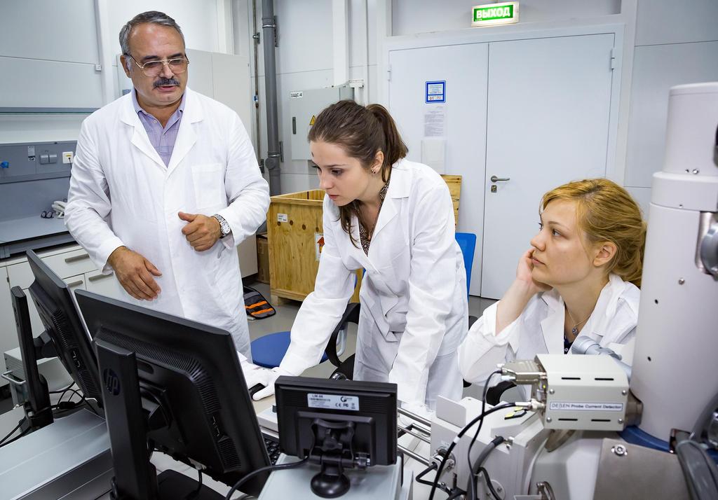
1 Scanning electron microscopy methods in study of micro objects Members : Ana-Maria Panaitescu Iuliana Taran University of Bucharest,Faculty of Physics Supervisor: Orelovich Oleg JINR Laboratory: FLNR
2
3 Scanning electron microscope-principles A scanning electron microscope (SEM) is a type of electron microscope that produces images of a sample by scanning it with a focused beam of electrons. The electrons interact with atoms in the sample, producing various signals that contain information about the sample's surface topography and composition. The electron beam is generally scanned in a raster scan pattern, and the beam's position is combined with the detected signal to produce an image. SEM can achieve the best resolution around 1 nanometer. Specimens can be observed in high vacuum, in low vacuum, in wet conditions (in environmental SEM), and at a wide range of cryogenic or elevated temperatures.
4 SEM principle/signals available from specimen
5 All samples must be of an appropriate size to fit in the specimen chamber and are generally mounted rigidly on a specimen holder called a specimen stage. Several models of SEM can examine any part of a 6-inch (15 cm) semiconductor wafer, and some can tilt an object of that size to 65. During the process of using the SEM it is possible to observe that the samples consist of different materials. In case the non-conductive specimen is investigated it is necessary to cover it with conductive layer. There are three general reasons for this operation: -the surface of sample must be electro conductive to minimize charging from initial beam; - the surface of sample must be thermo conductive to minimize local heating (as result of high density current in the influence area); -the material of sample must have high atomic number to increase the coefficient of secondary electron emission. First and second items can be assured by carbon layer on the sample surface. But a lot of secondary electrons can be provided from element with high number of electrons on the outer atomic levels (for example Cu, Ag, Au, Pt). In accordance to all these reasons the gold or platinum layers are most preferable.

6 The most special features of this scanning electron microscope are that it is truly a tabletop SEM, it is portable and it is designed for minimal preparation of specimens. The microscope is lightweight by design. The HITACHI TM3000 requires also low energy, just 550W. The HITACHI TM3000 is used for normal sized specimens. Characteristics Accelerating voltage: 5 or 15 kv, tungsten source Magnification: X 15 to X 30, nm resolution Backscattered detector only Charge reduction mode (which uses higher chamber pressure) allows imaging of uncoated samples Easy to use and portable

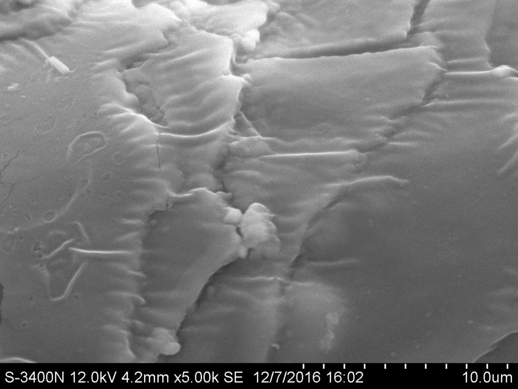
7 Instrument Specifications The Hitachi S-3400N SEM is a high performance, user-friendly scanning electron microscope with new improvements that allow the best results for a wide range of applications. Features include: Resolution -3.0nm High Vacuum Mode; -4.0nm Variable Pressure Mode. Chamber -Accomodates 10 inch specimen. Electron Gun -Variable Quad Bian Circuitry with Secondary Electrons (SE) Accelerator Plate Detectors-SE (Secondary Electrons); -BSE (Backscattered Secondary Electrons); -2 X-Ray detectors.

8 General Description: The Q150R system is a versatile magnetron sputter coater/carbon evaporator for preparing specimens for examination by electron microscopy. Q150R can be used to: Sputter coat samples using targets such as Gold or Platinum. Evaporate carbon support films for X-Ray analysis and conducting coatings for SEM using carbon cords. Glow discharge. We have used Q150R ES which is a combined system with interchangeable inserts for sputter coating or carbon evaporation. The instrument is fully adaptable to a wide range of specimens and offers easy loading and unloading of samples.


9 Standard sample for calibrating a microscope Sample:Planotec Sillicon test specimen mount C.
 Task: Capturing the image")

10 Calculus of parameteres of the membrane; the number of pores (the glossy side of a polymer foil ) Task: Capturing the image with the proper magnification that allows us to calculate the parameters of pores in order to calculate the density of pores.
11


12 The neccessity of using a conductive layer Comparison between sample with Au layer and sample without Au layer without gold


13 Polymer foil:polycarbonate Aim : to investigate the behaviour of foil with different structure on 2 sides - matte side and glossy side


14 Investigation of Z-contrast Carbon tape Gold layer Copper band Specimen stage


15 Cross section of a sample mounted on a special specimen stage Normal specimen stage Special specimen stage


16 Cross section of a sample mounted on a different specimen stage


17 Investigating salt particles on carbon tape (HITACHI TM3000) Salt particle on carbon tape salt crystals on carbon tape Salt particle on carbon tape


18 Investigating salt particles on carbon tape (HITACHI TM3000) Salt crystals on carbon tape Salt crystals on carbon tape


19 Investigating salt powder on carbon tape (HITACHI S 3400 N)

20 Investigation of natural dark hair


21 Investigation of blonde dyed hair Black part

22 Investigation of blonde dyed hair Black part


23 Investigation of an eyelash


24 Investigation of mascara eyelash


25 The use of gonyometre for the investigation of relief features 30 tilt 60 tilt The general view of the sample surface area
26
27 Scanning electron microscopy is widely employed to determine the structural characteristics of various materials like crystals, amorphous materials, polymers and microfiltering membranes. Comprehensive information on the membrane structure can be obtained by analyzing the images of both the membrane surfaces and cross sections. Electron microscopy is helpful for offering information regarding the elemental composition by collecting the X-Ray characteristic radiation spectrum.
28 Thank you for your attention!
Ion Beam Sputtering: Practical Applications to Electron Microscopy
 Ion Beam Sputtering: Practical Applications to Electron Microscopy Applications Laboratory Report Introduction Electron microscope specimens, both scanning (SEM) and transmission (TEM), often require a
The Basics of Scanning Electron Microscopy
 The Basics of Scanning Electron Microscopy The small scanning electron microscope is easy to use because almost every variable is pre-set: the acceleration voltage is always 15kV, it has only a single
Nanometer-scale imaging and metrology, nano-fabrication with the Orion Helium Ion Microscope
 andras@nist.gov Nanometer-scale imaging and metrology, nano-fabrication with the Orion Helium Ion Microscope Bin Ming, András E. Vladár and Michael T. Postek National Institute of Standards and Technology
Electron Microscopy 3. SEM. Image formation, detection, resolution, signal to noise ratio, interaction volume, contrasts
 Electron Microscopy 3. SEM Image formation, detection, resolution, signal to noise ratio, interaction volume, contrasts 3-1 SEM is easy! Just focus and shoot "Photo"!!! Please comment this picture... Any
Name: Due: September 21 st 2012. Physics 7230 Laboratory 3: High Resolution SEM Imaging
 Name: Due: September 21 st 2012 Physics 7230 Laboratory 3: High Resolution SEM Imaging 1. What is meant by the term resolution? How does this differ from other image variables, such as signal to noise
CSCI 4974 / 6974 Hardware Reverse Engineering. Lecture 8: Microscopy and Imaging
 CSCI 4974 / 6974 Hardware Reverse Engineering Lecture 8: Microscopy and Imaging Data Acquisition for RE Microscopy Imaging Registration and stitching Microscopy Optical Electron Scanning Transmission Scanning
Electron Microscopy SEM and TEM
 Electron Microscopy SEM and TEM Content 1. Introduction: Motivation for electron microscopy 2. Interaction with matter 3. SEM: Scanning Electron Microscopy 3.1 Functional Principle 3.2 Examples 3.3 EDX
View of ΣIGMA TM (Ref. 1)
") Overview of the FESEM system 1. Electron optical column 2. Specimen chamber 3. EDS detector [Electron Dispersive Spectroscopy] 4. Monitors 5. BSD (Back scatter detector) 6. Personal Computer 7. ON/STANDBY/OFF
Overview of the FESEM system 1. Electron optical column 2. Specimen chamber 3. EDS detector [Electron Dispersive Spectroscopy] 4. Monitors 5. BSD (Back scatter detector) 6. Personal Computer 7. ON/STANDBY/OFF
SALES SPECIFICATION. SC7640 Auto/Manual High Resolution Sputter Coater
 SALES SPECIFICATION SC7640 Auto/Manual High Resolution Sputter Coater Document Number SS-SC7640 Issue 1 (01/02) Disclaimer The components and packages described in this document are mutually compatible
Usage of AFM, SEM and TEM for the research of carbon nanotubes
 Usage of AFM, SEM and TEM for the research of carbon nanotubes K.Safarova *1, A.Dvorak 2, R. Kubinek 1, M.Vujtek 1, A. Rek 3 1 Department of Experimental Physics, Faculty of Science, Palacky University,
7. advanced SEM. Latest generation of SEM SEM
 7. advanced SEM SEM Low voltage SE imaging Condition of the surface, coatings, plasma cleaning Low voltage BSE imaging Polishing for BSE, EDX and EBSD, effect of ion beam etching/polishing 1 Latest generation
Vacuum Evaporation Recap
 Sputtering Vacuum Evaporation Recap Use high temperatures at high vacuum to evaporate (eject) atoms or molecules off a material surface. Use ballistic flow to transport them to a substrate and deposit.
Scanning Electron Microscopy: an overview on application and perspective
 Scanning Electron Microscopy: an overview on application and perspective Elvio Carlino Center for Electron Microscopy - IOM-CNR Laboratorio Nazionale TASC - Trieste, Italy Location of the Center for Electron
Coating Technology: Evaporation Vs Sputtering
 Satisloh Italy S.r.l. Coating Technology: Evaporation Vs Sputtering Gianni Monaco, PhD R&D project manager, Satisloh Italy 04.04.2016 V1 The aim of this document is to provide basic technical information
Electron Microscopy 3. SEM. Image formation, detection, resolution, signal to noise ratio, interaction volume, contrasts
 Electron Microscopy 3. SEM Image formation, detection, resolution, signal to noise ratio, interaction volume, contrasts SEM is easy! Just focus and shoot "Photo"!!! Please comment this picture... Any idea
The Focused Ion Beam Scanning Electron Microscope: A tool for sample preparation, two and three dimensional imaging. Jacob R.
 The Focused Ion Beam Scanning Electron Microscope: A tool for sample preparation, two and three dimensional imaging Jacob R. Bowen Contents Components of a FIB-SEM Ion interactions Deposition & patterns
Introduktion til røntgenfluorescens (XRF) og skanning elektron mikroskopi (SEM) Michelle Taube Nationalmuseet Bevaringsafdelingen
 og skanning elektron mikroskopi (SEM) Michelle Taube Nationalmuseet Bevaringsafdelingen") Introduktion til røntgenfluorescens (XRF) og skanning elektron mikroskopi (SEM) Michelle Taube Nationalmuseet Bevaringsafdelingen Introduktion til røntgenfluorescens (XRF) og skanning elektron mikroskopi
Introduktion til røntgenfluorescens (XRF) og skanning elektron mikroskopi (SEM) Michelle Taube Nationalmuseet Bevaringsafdelingen Introduktion til røntgenfluorescens (XRF) og skanning elektron mikroskopi
BIOACTIVE COATINGS ON 316L STAINLESS STEEL IMPLANTS
 Trends Biomater. Artif. Organs. Vol. 17(2) pp 43-47 (2004) http//www.sbaoi.org BIOACTIVE COATINGS ON 316L STAINLESS STEEL IMPLANTS N. Ramesh Babu*,+, Sushant Manwatkar*, K. Prasada Rao* and T. S. Sampath
VCR Ion Beam Sputter Coater
 VCR Ion Beam Sputter Coater Sputtering Process and Rates 2 Vacuum System 3 Loading the Sputter Chamber 4 Sputter Coating 5 Removing Samples from Chamber 6 Appendix A: VCR High Vacuum Gauge Conditioning
Lecture 6 Scanning Tunneling Microscopy (STM) General components of STM; Tunneling current; Feedback system; Tip --- the probe.
 General components of STM; Tunneling current; Feedback system; Tip --- the probe.") Lecture 6 Scanning Tunneling Microscopy (STM) General components of STM; Tunneling current; Feedback system; Tip --- the probe. Brief Overview of STM Inventors of STM The Nobel Prize in Physics 1986 Nobel
Lecture 6 Scanning Tunneling Microscopy (STM) General components of STM; Tunneling current; Feedback system; Tip --- the probe. Brief Overview of STM Inventors of STM The Nobel Prize in Physics 1986 Nobel
Scanning Electron Microscopy Primer
 Scanning Electron Microscopy Primer Bob Hafner This primer is intended as background for the Introductory Scanning Electron Microscopy training offered by the University of Minnesota s Characterization
h e l p s y o u C O N T R O L
 contamination analysis for compound semiconductors ANALYTICAL SERVICES B u r i e d d e f e c t s, E v a n s A n a l y t i c a l g r o u p h e l p s y o u C O N T R O L C O N T A M I N A T I O N Contamination
Coating Thickness and Composition Analysis by Micro-EDXRF
 Application Note: XRF Coating Thickness and Composition Analysis by Micro-EDXRF www.edax.com Coating Thickness and Composition Analysis by Micro-EDXRF Introduction: The use of coatings in the modern manufacturing
Supporting Information
 Supporting Information Wiley-VCH 2005 69451 Weinheim, Germany Magnetic Nanoparticle-Capped Mesoporous Silica Nanorod-Based Stimuli-Responsive Controlled Release Delivery System** Supratim Giri, Brian G.
PHYSICAL METHODS, INSTRUMENTS AND MEASUREMENTS Vol. III - Surface Characterization - Marie-Geneviève Barthés-Labrousse
 SURFACE CHARACTERIZATION Marie-Geneviève Centre d Etudes de Chimie Métallurgique, CNRS, Vitry-sur-Seine, France Keywords: Surface Analysis, Surface imaging, Surface composition, Surface chemical analysis,
BB-18 Black Body High Vacuum System Technical Description
 BB-18 Black Body High Vacuum System Technical Description The BB-18 Black Body is versatile and is programmed for use as a fixed cold target at 80 K or variable target, at 80 K- 350 K no extra cost. The
Atomic Force Microscopy. Long Phan Nanotechnology Summer Series May 15, 2013
 Atomic Force Microscopy Long Phan Nanotechnology Summer Series May 15, 2013 1 World s Smallest Movie 2 Outline What is AFM? How does AFM Work? 3 Modes: Contact mode Non contact mode Tapping mode Imaging
Testing and characterization of anti-reflection coatings on glass
 Testing and characterization of anti-reflection coatings on glass Diagnostic approaches at CSP M.Turek, M. Dyrba, S. Großer, V. Naumann, Ch. Hagendorf contact: marko.turek@csp.fraunhofer.de Tests and methods
Super Cool Sputter Coater
 Leica EM SCD050 Super Cool Sputter Coater Precious and Non-Precious Metal Sputtering and Carbon Evaporation Sputter Coating The sputter coating of samples inhibits charging, reduces thermal damage and
Leica EM SCD500. High Vacuum Sputter Coater For Highest Resolution FE-SEM Analysis
 Leica EM SCD500 High Vacuum Sputter Coater For Highest Resolution FE-SEM Analysis High Vacuum Sputter Coating The Leica EM SCD500 is a versatile high vacuum film deposition system designed to produce very
for Low power Energy Harvesting Sun to fiber' Solar Devices
 Nanostructured Energy Conversion for Low power Energy Harvesting Devices and Beyond for High power Sun to fiber' Solar Devices Michael Oye and Nobuhiko Nobby Kobayashi Advanced Studies Laboratories and
THERMO NORAN SYSTEM SIX ENERGY DISPERSIVE X- RAY SPECTROMETER. Insert Nickname Here. Operating Instructions
 THERMO NORAN SYSTEM SIX ENERGY DISPERSIVE X- RAY SPECTROMETER Insert Nickname Here Operating Instructions Table of Contents 1 INTRODUCTION Safety 1 Samples 1 2 BACKGROUND Background Information 3 References
2. Deposition process
 Properties of optical thin films produced by reactive low voltage ion plating (RLVIP) Antje Hallbauer Thin Film Technology Institute of Ion Physics & Applied Physics University of Innsbruck Investigations
Demonstration of sub-4 nm nanoimprint lithography using a template fabricated by helium ion beam lithography
 Demonstration of sub-4 nm nanoimprint lithography using a template fabricated by helium ion beam lithography Wen-Di Li*, Wei Wu** and R. Stanley Williams Hewlett-Packard Labs *Current address: University
Use the BET (after Brunauer, Emmett and Teller) equation is used to give specific surface area from the adsorption
 equation is used to give specific surface area from the adsorption") Number of moles of N 2 in 0.129dm 3 = 0.129/22.4 = 5.76 X 10⁻³ moles of N 2 gas Module 8 : Surface Chemistry Objectives Lecture 37 : Surface Characterization Techniques After studying this lecture, you
Number of moles of N 2 in 0.129dm 3 = 0.129/22.4 = 5.76 X 10⁻³ moles of N 2 gas Module 8 : Surface Chemistry Objectives Lecture 37 : Surface Characterization Techniques After studying this lecture, you
BNG 331 Cell-Tissue Material Interactions. Biomaterial Surfaces
 BNG 331 Cell-Tissue Material Interactions Biomaterial Surfaces Course update Updated syllabus Homework 4 due today LBL 5 Friday Schedule for today: Chapter 8 Biomaterial surface characterization Surface
Preface Light Microscopy X-ray Diffraction Methods
 Preface xi 1 Light Microscopy 1 1.1 Optical Principles 1 1.1.1 Image Formation 1 1.1.2 Resolution 3 1.1.3 Depth of Field 5 1.1.4 Aberrations 6 1.2 Instrumentation 8 1.2.1 Illumination System 9 1.2.2 Objective
Forensic Science: The Basics. Microscopy
 Forensic Science: The Basics Microscopy Chapter 6 Jay A. Siegel,Ph.D. Power point presentation by Greg Galardi, Peru State College, Peru Nebraska Presentation by Greg Galardi, Peru State College CRC Press,
FEI Forensic Systems. Choose your armory for the next decade
 FEI Forensic Systems Choose your armory for the next decade 1 Choose your armory for the next decade Forensic Quanta High vacuum, low vacuum and environmental SEM (ESEM ) GSR S50 SEM for automated analysis
Phase Characterization of TiO 2 Powder by XRD and TEM
 Kasetsart J. (Nat. Sci.) 42 : 357-361 (28) Phase Characterization of TiO 2 Powder by XRD and TEM Kheamrutai Thamaphat 1 *, Pichet Limsuwan 1 and Boonlaer Ngotawornchai 2 ABSTRACT In this study, the commercial
The photoionization detector (PID) utilizes ultraviolet
 utilizes ultraviolet") Chapter 6 Photoionization Detectors The photoionization detector (PID) utilizes ultraviolet light to ionize gas molecules, and is commonly employed in the detection of volatile organic compounds (VOCs).
Chapter 6 Photoionization Detectors The photoionization detector (PID) utilizes ultraviolet light to ionize gas molecules, and is commonly employed in the detection of volatile organic compounds (VOCs).
www.axon-cable.com Power distribution systems
 www.axon-cable.com Power distribution systems Power distribution systems As vital components for electrical power distribution in telecommunication satellites and landbased weapon systems, the bus and
Scanning He + Ion Beam Microscopy and Metrology. David C Joy University of Tennessee, and Oak Ridge National Laboratory
 Scanning He + Ion Beam Microscopy and Metrology David C Joy University of Tennessee, and Oak Ridge National Laboratory The CD-SEM For thirty years the CD-SEM has been the tool for metrology But now, as
1. Photon Beam Damage and Charging at Solid Surfaces John H. Thomas III
 1. Photon Beam Damage and Charging at Solid Surfaces John H. Thomas III 1. Introduction............................. 2. Electrostatic Charging of Samples in Photoemission Experiments............................
Raman and AFM characterization of carbon nanotube polymer composites Illia Dobryden
 Raman and AFM characterization of carbon nanotube polymer composites Illia Dobryden This project is conducted in High Pressure Spectroscopy Laboratory (Materials Physics group) Supervisor: Professor Alexander
Chapter 4. Microscopy, Staining, and Classification. Lecture prepared by Mindy Miller-Kittrell North Carolina State University
 Chapter 4 Microscopy, Staining, and Classification 2012 Pearson Education Inc. Lecture prepared by Mindy Miller-Kittrell North Carolina State University Microscopy and Staining 2012 Pearson Education Inc.
Lateral Resolution of EDX Analysis with Low Acceleration Voltage SEM
 Original Paper Lateral Resolution of EDX Analysis with Low Acceleration Voltage SEM Satoshi Hashimoto 1, Tsuguo Sakurada 1, and Minoru Suzuki 2 1 JFE-Techno research corporation, 1-1 Minamiwatarida, Kawasaki,
The OPERA Emulsions. Jan Lenkeit. Hamburg Student Seminar, 12 June 2008. Institut für Experimentalphysik Forschungsgruppe Neutrinophysik
 The OPERA Emulsions Jan Lenkeit Institut für Experimentalphysik Forschungsgruppe Neutrinophysik Hamburg Student Seminar, 12 June 2008 1/43 Outline The OPERA experiment Nuclear emulsions The OPERA emulsions
BAL-TEC SCD 005. Scientist in charge: Lhoussaine Belkoura 07/14/06. softcomp soft matter composites 1
 07/14/06 softcomp soft matter composites 1 BAL-TEC SCD 005 Institution: University of Cologne Scientist in charge: Lhoussaine Belkoura SCD 005 Cool Sputter Coater 26.02.99 Internet: www.bal-tec.com & 1
The Effect of Coating Process Conditions and Coating Formula Type on the Quantity and Location of Water in Film Coated Tablets
 OPADRY II Application Data High Performance Film Coating System The Effect of Coating Process Conditions and Coating Formula Type on the Quantity and Location of Water in Film Coated Tablets OBJECTIVES
Lectures about XRF (X-Ray Fluorescence)
") 1 / 38 Lectures about XRF (X-Ray Fluorescence) Advanced Physics Laboratory Laurea Magistrale in Fisica year 2013 - Camerino 2 / 38 X-ray Fluorescence XRF is an acronym for X-Ray Fluorescence. The XRF technique
1 / 38 Lectures about XRF (X-Ray Fluorescence) Advanced Physics Laboratory Laurea Magistrale in Fisica year 2013 - Camerino 2 / 38 X-ray Fluorescence XRF is an acronym for X-Ray Fluorescence. The XRF technique
Microhardness study of Ti(C, N) films deposited on S-316 by the Hallow Cathode Discharge Gun
 films deposited on S-316 by the Hallow Cathode Discharge Gun") of Achievements in Materials and Manufacturing Engineering VOLUME 14 ISSUE 1-2 January-February 2006 Microhardness study of Ti(C, N) films deposited on S-316 by the Hallow Cathode Discharge Gun A.J. Novinrooz*,
of Achievements in Materials and Manufacturing Engineering VOLUME 14 ISSUE 1-2 January-February 2006 Microhardness study of Ti(C, N) films deposited on S-316 by the Hallow Cathode Discharge Gun A.J. Novinrooz*,
Polymer growth rate in a wire chamber with oxygen, water, or alcohol gas additives
 SLAC-PUB-13 June 6, 8 Polymer growth rate in a wire chamber with oxygen, water, or alcohol gas additives Adam M. Boyarski Stanford Linear Accelerator Center, M.S. 95, 575 Sand Hill Rd, Menlo Park, CA 95,
Nanoparticle Deposition on Packaging Materials by the Liquid Flame Spray
 Nanoparticle Deposition on Packaging Materials by the Liquid Flame Spray Hannu Teisala a, Mikko Tuominen a, Mikko Aromaa b, Jyrki M. Mäkelä b, Milena Stepien c, Jarkko J. Saarinen c, Martti Toivakka c
Introduction to the Scanning Electron Microscope
 Introduction to the Scanning Electron Microscope Theory, Practice, & Procedures Prepared by Michael Dunlap & Dr. J. E. Adaskaveg Presented by the FACILITY FOR ADVANCED INSTRUMENTATION, U. C. Davis 1997
Micro-CT for SEM Non-destructive Measurement and Volume Visualization of Specimens Internal Microstructure in SEM Micro-CT Innovation with Integrity
 Micro-CT for SEM Non-destructive Measurement and Volume Visualization of Specimens Internal Microstructure in SEM Innovation with Integrity Micro-CT 3D Microscopy Using Micro-CT for SEM Micro-CT for SEM
THIN FILM MATERIALS TECHNOLOGY
 THIN FILM MATERIALS TECHNOLOGY Sputtering of Compound Materials by Kiyotaka Wasa Yokohama City University Yokohama, Japan Makoto Kitabatake Matsushita Electric Industrial Co., Ltd. Kyoto, Japan Hideaki
Lecture 4 Scanning Probe Microscopy (SPM)
") Lecture 4 Scanning Probe Microscopy (SPM) General components of SPM; Tip --- the probe; Cantilever --- the indicator of the tip; Tip-sample interaction --- the feedback system; Scanner --- piezoelectric
Lecture 4 Scanning Probe Microscopy (SPM) General components of SPM; Tip --- the probe; Cantilever --- the indicator of the tip; Tip-sample interaction --- the feedback system; Scanner --- piezoelectric
CALCULATION METHODS OF X-RAY SPECTRA: A COMPARATIVE STUDY
 243 CALCULATION METHODS OF X-RAY SPECTRA: A COMPARATIVE STUDY B. Chyba, M. Mantler, H. Ebel, R. Svagera Technische Universit Vienna, Austria ABSTRACT The accurate characterization of the spectral distribution
X-RAY TUBE SELECTION CRITERIA FOR BGA / CSP X-RAY INSPECTION
 X-RAY TUBE SELECTION CRITERIA FOR BGA / CSP X-RAY INSPECTION David Bernard Dage Precision Industries Inc. Fremont, California d.bernard@dage-group.com ABSTRACT The x-ray inspection of PCB assembly processes
FEATURES AND BENEFITS OF DIFFERENT PLATINUM ALLOYS. Kris Vaithinathan and Richard Lanam Engelhard Corporation
 FEATURES AND BENEFITS OF DIFFERENT PLATINUM ALLOYS Kris Vaithinathan and Richard Lanam Engelhard Corporation Introduction There has been a significant increase in the world wide use of platinum for jewelry
Optical Microscope; Scanning Electron Microscope (SEM); Transmission Electron Microscope (TEM);
; Transmission Electron Microscope (TEM);") Lecture 3 Brief Overview of Traditional Microscopes Optical Microscope; Scanning Electron Microscope (SEM); Transmission Electron Microscope (TEM); Comparison with scanning probe microscope (SPM) General
Lecture 3 Brief Overview of Traditional Microscopes Optical Microscope; Scanning Electron Microscope (SEM); Transmission Electron Microscope (TEM); Comparison with scanning probe microscope (SPM) General
DIEGO TONINI MORPHOLOGY OF NIOBIUM FILMS SPUTTERED AT DIFFERENT TARGET SUBSTRATE ANGLE
 UNIVERSITÀ DEGLI STUDI DI PADOVA SCIENCE FACULTY MATERIAL SCIENCE DEGREE INFN LABORATORI NAZIONALI DI LEGNARO DIEGO TONINI MORPHOLOGY OF NIOBIUM FILMS SPUTTERED AT DIFFERENT TARGET SUBSTRATE ANGLE 2 QUESTIONS
Luminescence study of structural changes induced by laser cutting in diamond films
 Luminescence study of structural changes induced by laser cutting in diamond films A. Cremades and J. Piqueras Departamento de Fisica de Materiales, Facultad de Fisicas, Universidad Complutense, 28040
Near-field scanning optical microscopy (SNOM)
") Adviser: dr. Maja Remškar Institut Jožef Stefan January 2010 1 2 3 4 5 6 Fluorescence Raman and surface enhanced Raman 7 Conventional optical microscopy-limited resolution Two broad classes of techniques
Adviser: dr. Maja Remškar Institut Jožef Stefan January 2010 1 2 3 4 5 6 Fluorescence Raman and surface enhanced Raman 7 Conventional optical microscopy-limited resolution Two broad classes of techniques
GD-Profiler Series RF Glow Discharge Optical Emission Spectrometers
 GD-Profiler Series RF Glow Discharge Optical Emission Spectrometers For many applications, it is essential to know the chemical composition of a material, both at the surface, at the interfaces and in
Microscopy. MICROSCOPY Light Electron Tunnelling Atomic Force RESOLVE: => INCREASE CONTRAST BIODIVERSITY I BIOL1051 MAJOR FUNCTIONS OF MICROSCOPES
 BIODIVERSITY I BIOL1051 Microscopy Professor Marc C. Lavoie marc.lavoie@cavehill.uwi.edu MAJOR FUNCTIONS OF MICROSCOPES MAGNIFY RESOLVE: => INCREASE CONTRAST Microscopy 1. Eyepieces 2. Diopter adjustment
INTRODUCTION TO THE XL30-FEG SEM. 1.1 The mouse. 1.2. The monitor. Figure 1.1 1. THE USER INTERFACE
 INTRODUCTION TO THE XL30-FEG SEM All software used to control the microscope runs in the MS-Windows environment. This environment is loaded on the Windows2000 operating system. However, it is not really
Microscopy and Nanoindentation. Combining Orientation Imaging. to investigate localized. deformation behaviour. Felix Reinauer
 Combining Orientation Imaging Microscopy and Nanoindentation to investigate localized deformation behaviour Felix Reinauer René de Kloe Matt Nowell Introduction Anisotropy in crystalline materials Presentation
From ideas to implementation
 Physics HSC Course Stage 6 From ideas to implementation Part 2: The amazing cathode ray tube Contents Introduction... 2 Cathode ray tubes (CRT)... 3 Types of cathode ray tube...3 What makes up a CRT?...4
Hitachi U-4100 UV-vis-NIR spectrophotometer (341-F)
") Hitachi U-4100 UV-vis-NIR spectrophotometer (341-F) Please contact Dr. Amanda Young for training requests and assistance: 979-862-6845, amandayoung@tamu.edu Hardware Our spectrophotometer is made up of
Hitachi U-4100 UV-vis-NIR spectrophotometer (341-F) Please contact Dr. Amanda Young for training requests and assistance: 979-862-6845, amandayoung@tamu.edu Hardware Our spectrophotometer is made up of
Le nanotecnologie: dal Laboratorio al Mercato. Fabrizio Pirri Politecnico di Torino Istituto Italiano di Tecnologia
 Le nanotecnologie: dal Laboratorio al Mercato Fabrizio Pirri Politecnico di Torino Istituto Italiano di Tecnologia Materials & Processes for micro nanotechnologies Laboratory http://www.polito.it/micronanotech
Evaluating Surface Roughness of Si Following Selected Lapping and Polishing Processes
 Applications Laboratory Report 86 Evaluating Surface Roughness of Si Following Selected Processes Purpose polishing of samples is a common application and required for a variety of manufacturing and research
Conductivity of silicon can be changed several orders of magnitude by introducing impurity atoms in silicon crystal lattice.
 CMOS Processing Technology Silicon: a semiconductor with resistance between that of conductor and an insulator. Conductivity of silicon can be changed several orders of magnitude by introducing impurity
Results Overview Wafer Edge Film Removal using Laser
 Results Overview Wafer Edge Film Removal using Laser LEC- 300: Laser Edge Cleaning Process Apex Beam Top Beam Exhaust Flow Top Beam Scanning Top & Top Bevel Apex Beam Scanning Top Bevel, Apex, & Bo+om
Cambridge International Examinations Cambridge International General Certificate of Secondary Education
 Cambridge International Examinations Cambridge International General Certificate of Secondary Education *0123456789* PHYSICS 0625/04 Paper 4 Theory (Extended) For Examination from 2016 SPECIMEN PAPER 1
Lecture 12. Physical Vapor Deposition: Evaporation and Sputtering Reading: Chapter 12. ECE 6450 - Dr. Alan Doolittle
 Lecture 12 Physical Vapor Deposition: Evaporation and Sputtering Reading: Chapter 12 Evaporation and Sputtering (Metalization) Evaporation For all devices, there is a need to go from semiconductor to metal.
Scanning Electron Microscopy Services for Pharmaceutical Manufacturers
 Scanning Electron Microscopy Services for Pharmaceutical Manufacturers Author: Gary Brake, Marketing Manager Date: August 1, 2013 Analytical Testing Laboratory www.atl.semtechsolutions.com Scanning Electron
OPTIMIZING OF THERMAL EVAPORATION PROCESS COMPARED TO MAGNETRON SPUTTERING FOR FABRICATION OF TITANIA QUANTUM DOTS
 OPTIMIZING OF THERMAL EVAPORATION PROCESS COMPARED TO MAGNETRON SPUTTERING FOR FABRICATION OF TITANIA QUANTUM DOTS Vojtěch SVATOŠ 1, Jana DRBOHLAVOVÁ 1, Marian MÁRIK 1, Jan PEKÁREK 1, Jana CHOMOCKÁ 1,
Combustion chemical vapor deposition
 V I P Combustion chemical vapor deposition A technology to improve adhesion on surfaces to be coated Volkmar J. Eigenbrod, Christina Hensch, Alexander Kemper Introduction Combustion chemical vapor deposition
Institute s brochure. Microstructure Analysis, Metallography and Mechanical Testing of Materials. Institute of Materials Research
 Institute s brochure Microstructure Analysis, Metallography and Mechanical Testing of Materials Institute of Materials Research Micro structure Analysis and Metallography is one of the core teams of the
Mass production, R&D Failure analysis. Fault site pin-pointing (EM, OBIRCH, FIB, etc. ) Bottleneck Physical science analysis (SEM, TEM, Auger, etc.
 Bottleneck Physical science analysis (SEM, TEM, Auger, etc.") Failure Analysis System for Submicron Semiconductor Devices 68 Failure Analysis System for Submicron Semiconductor Devices Munetoshi Fukui Yasuhiro Mitsui, Ph. D. Yasuhiko Nara Fumiko Yano, Ph. D. Takashi
Failure Analysis System for Submicron Semiconductor Devices 68 Failure Analysis System for Submicron Semiconductor Devices Munetoshi Fukui Yasuhiro Mitsui, Ph. D. Yasuhiko Nara Fumiko Yano, Ph. D. Takashi
STM and AFM Tutorial. Katie Mitchell January 20, 2010
 STM and AFM Tutorial Katie Mitchell January 20, 2010 Overview Scanning Probe Microscopes Scanning Tunneling Microscopy (STM) Atomic Force Microscopy (AFM) Contact AFM Non-contact AFM RHK UHV350 AFM/STM
Scanning Near-Field Optical Microscopy for Measuring Materials Properties at the Nanoscale
 Scanning Near-Field Optical Microscopy for Measuring Materials Properties at the Nanoscale Outline Background Research Design Detection of Near-Field Signal Submonolayer Chemical Sensitivity Conclusions
bulk 5. Surface Analysis Why surface Analysis? Introduction Methods: XPS, AES, RBS
 5. Surface Analysis Introduction Methods: XPS, AES, RBS Autumn 2011 Experimental Methods in Physics Marco Cantoni Why surface Analysis? Bulk: structural function Electrical/thermal conduction Volume increases
Introduction to VLSI Fabrication Technologies. Emanuele Baravelli
 Introduction to VLSI Fabrication Technologies Emanuele Baravelli 27/09/2005 Organization Materials Used in VLSI Fabrication VLSI Fabrication Technologies Overview of Fabrication Methods Device simulation
Scanning Electron Microscopy tools for material characterization
 5th International Workshop on Mechanisms of Vacuum Arcs 02-04/09/2015 Scanning Electron Microscopy tools for material characterization Focus on EBSD for characterisation of dislocation structures Floriane
DETECTION OF COATINGS ON PAPER USING INFRA RED SPECTROSCOPY
 DETECTION OF COATINGS ON PAPER USING INFRA RED SPECTROSCOPY Eduard Gilli 1,2 and Robert Schennach 1, 2 1 Graz University of Technology, 8010 Graz, Austria 2 CD-Laboratory for Surface Chemical and Physical
DualBeam Solutions for Electrical Nanoprobing
 DualBeam Solutions for Electrical Nanoprobing Richard J. Young, Technologist Peter D. Carleson, Product Marketing Engineer Electrical testing by physically probing device structures has grown more challenging
Standard Test Method for Classification of Film Systems for Industrial Radiography 1
 Designation: E 1815 96 (Reapproved 2001) Standard Test Method for Classification of Film Systems for Industrial Radiography 1 This standard is issued under the fixed designation E 1815; the number immediately
NATIONAL NETWORK OF ELECTRON MICROSCOPY RNME. NETWORK MANAGEMENT MODEL a ARTICULATION AND GENERAL OPERATION. (English translation draft)
") NATIONAL NETWORK OF ELECTRON MICROSCOPY RNME NETWORK MANAGEMENT MODEL a ARTICULATION AND GENERAL OPERATION (English translation draft) 1. Introduction 2 2. Objectives 2 3. Constitution 2 4. Organization
NATIONAL NETWORK OF ELECTRON MICROSCOPY RNME NETWORK MANAGEMENT MODEL a ARTICULATION AND GENERAL OPERATION (English translation draft) 1. Introduction 2 2. Objectives 2 3. Constitution 2 4. Organization
PHYA5/1. General Certificate of Education Advanced Level Examination June 2012. Unit 5 Nuclear and Thermal Physics Section A
 Centre Number Surname Candidate Number For Examinerʼs Use Other Names Candidate Signature Examinerʼs Initials General Certificate of Education Advanced Level Examination June 2012 Question 1 2 Mark Physics
Balzers Sputter Coater SCD 050
 Balzers Sputter Coater SCD 050 The SCD 050 is a bench top, sputter deposition system designed for thin films on substrates up to 6 inches. Morphology and thickness is user controlled using power, pressure,
Physics 441/2: Transmission Electron Microscope
 Physics 441/2: Transmission Electron Microscope Introduction In this experiment we will explore the use of transmission electron microscopy (TEM) to take us into the world of ultrasmall structures. This
Energy Dispersive Spectroscopy on the SEM: A Primer
 Energy Dispersive Spectroscopy on the SEM: A Primer Bob Hafner This primer is intended as background for the EDS Analysis on the SEM course offered by the University of Minnesota s Characterization Facility.
Instrumentation. (Figure 2)
") X-Ray Fluorescence Lab Report Nydia Esparza Victoria Rangel Physics of XRF XRF is a non destructive analytical technique that is used for elemental and chemical analysis. X-Ray Fluorescence Spectroscopy
X-Ray Fluorescence Lab Report Nydia Esparza Victoria Rangel Physics of XRF XRF is a non destructive analytical technique that is used for elemental and chemical analysis. X-Ray Fluorescence Spectroscopy
CHAPTER 2 EXPERIMENTAL. g/mol, Sigma-Aldrich, Germany. 2.1.2 Magnesium acetate tetrahydrate (C 4 H 6 MgO. 4 4H 2 O), assay 99.0%,
, assay 99.0%,") CHAPTER 2 EXPERIMENTAL 2.1 Chemicals and Equipments 2.1.1 Zinc naphthenate (2(C 11 H 7 O 2 ). Zn), assay
CHAPTER 2 EXPERIMENTAL 2.1 Chemicals and Equipments 2.1.1 Zinc naphthenate (2(C 11 H 7 O 2 ). Zn), assay
Usage of Carbon Nanotubes in Scanning Probe Microscopes as Probe. Keywords: Carbon Nanotube, Scanning Probe Microscope
 International Journal of Arts and Sciences 3(1): 18-26 (2009) CD-ROM. ISSN: 1944-6934 InternationalJournal.org Usage of Carbon Nanotubes in Scanning Probe Microscopes as Probe Bedri Onur Kucukyildirim,
Properties of Electrons, their Interactions with Matter and Applications in Electron Microscopy
 Properties of Electrons, their Interactions with Matter and Applications in Electron Microscopy By Frank Krumeich Laboratory of Inorganic Chemistry, ETH Zurich, Vladimir-Prelog-Weg 1, 8093 Zurich, Switzerland
Hygro-Thermometer + InfraRed Thermometer Model RH101
 User's Guide Hygro-Thermometer + InfraRed Thermometer Model RH101 Introduction Congratulations on your purchase of the Extech Hygro-Thermometer plus InfraRed Thermometer. This device measures relative