Lecture 4 Scanning Probe Microscopy (SPM)
|
|
|
- Vernon Waters
- 7 years ago
- Views:
Transcription
1 Lecture 4 Scanning Probe Microscopy (SPM) General components of SPM; Tip --- the probe; Cantilever --- the indicator of the tip; Tip-sample interaction --- the feedback system; Scanner --- piezoelectric movement at x,y,z; Measurement artifacts: vibration must be isolated.

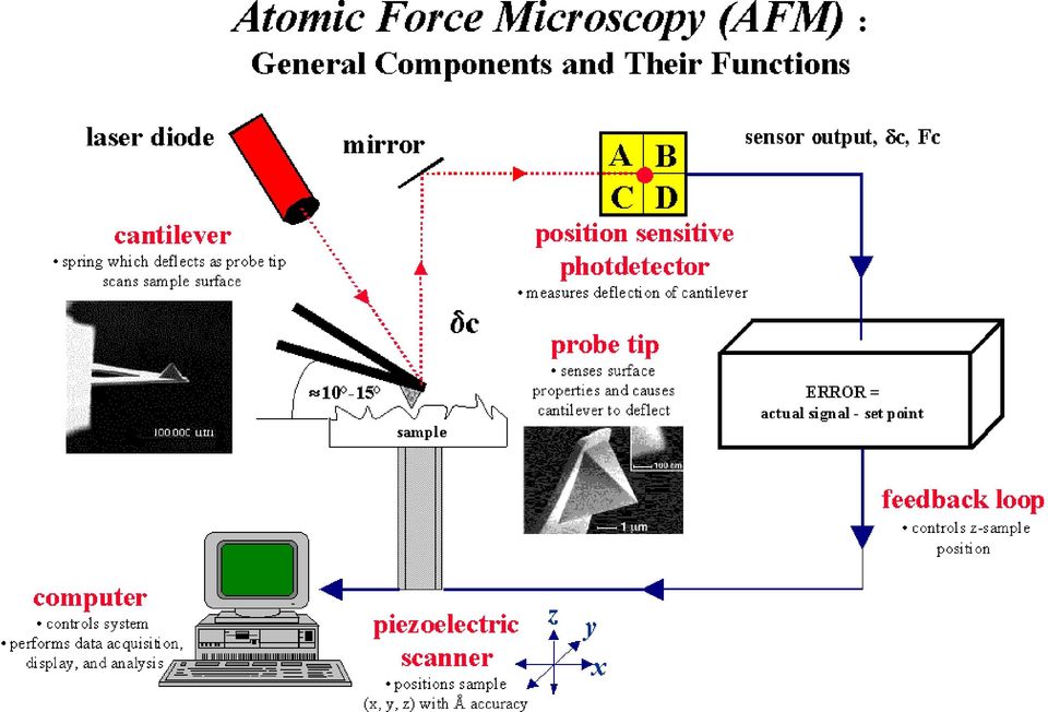
2 Basic components of SPM: tip, cantilever, sensor for tip positioning, scanner, feedback loop (electronic control)

3 Generation of SPM image X-Y raster scanning; Z-modulation (height) by feedback system.
")
4 SPM Family Tip-Sample Electrical Current SPM Tip-Sample Interaction AFM + Optical Microscopy STM AFM NSOM Extremely high Resolution at UHV. Mechanic Force: Contact mode Non-contact mode Tapping (intermittent) mode Other Interactions: Electrostatic mode (scanning electrostatic potential microscope) Magnetic mode Chemical Force mode Scanning Confocal
 Magnetic")
5 Basic components of STM: The scanner can be mounted with the tip or the sample stage. Five basic components: 1. Metal tip, 2. Piezoelectric scanner, 3. Current amplifier (na), 4. Bipotentiostat (bias), 5. Feedback loop (current). Tunneling current from tip to sample or vice-versa depending on bias; Current is exponentially dependent on distance; Raster scanning gives 2D image; Feedback is normally based on constant current, thus measuring the height on surface.

6
7 Scanning Confocal Microscopy from NSOM NSOM can be modified to be a SCM simply by removing the tuning fork head, the tip. SCM uses the excitation beam through the same objective. Both the excitation and emission shares the same focus on the sample surface. Confocal requires high level alignment of optical accessories.

8 Co-focus Principle of Scanning Confocal Microscope

9 Comparison of STM, AFM, NSOM STM NSOM AFM

10 Comparison of Tips of STM, AFM, NSOM STM tip should be conducting, can be simply cut freshly by normal wire cutter. STM plays with the very top atom at the freshly cut tip, leading to atomic resolution. AFM tip should be sharp enough to get good resolution (fat-tip effect); recently atomically sharp tip obtained by binding a small molecule atop the tip. AFM tip should be stiff enough to sense the atomic interaction with sample surface (the distance). AFM tip is not necessary to be conducting. NSOM tip should be sharp enough to get good topography resolution. The aperture of NSOM tip should be small for better optical resolution. The outer surface of NSOM tip should be flat to avoid artificial effects from the scanning.
. AFM tip is not necessary to be conducting.")
11 Brief History of Scanning Probe Microscopy (SPM): 1 The first member of SPM family, scanning tunneling microscopy (STM), was developed in 1980s. In 1982, Gerd Binnig and Heinrich Rohrer at IBM in Zurich created the ideas of STM (Phys. Rev. Lett., 1982, vol 49, p57). Both of the two people won 1986 Nobel prize in physics for their brilliant invention. The Nobel Prize in Physics 2000 Heinrich Rohrer and Gerd Binnig
.")
12 Brief History of Scanning Probe Microscopy (SPM): STM

13 Brief History of Scanning Probe Microscopy (SPM): AFM

14 Cantilever: indicating the tip motion and rotation Laser sensing to monitor the position of cantilever: 1. Contact mode scanning: cantilever is usually not vibrating, but deflected due to friction or other forces. Such a deflection can be detected precisely by the sensitive photodiode. 2. Non-contact mode scanning: cantilever is in vibration with constant frequency (> 100 khz). Such vibration can be monitored precisely by the laser sensing. To keep the resonance frequency (the constant height over the sample) during scanning, the Z-scanner has to adjust the height of the cantilever. Such adjustment can be recorded by the computer to create the scanning profile, the image.

15 Laser sensing both tilting and twisting of cantilever

16 How to create vibration of cantilever? There are two ways to drive the cantilever into oscillation. One way is accomplished by indirect vibration, in which the cantilever is excited by high frequency acoustic vibration from a piezoelectric transducer attached to the cantilever holder. This is called the Acoustic AC mode (AAC). Another, more favored method that is much cleaner and gentler than Acoustic AC mode is a direct vibration method where the cantilever is excited directly without having to vibrate the cantilever housing or other parts. This is called Magnetic AC mode (MAC Mode ). To achieve MAC Mode imaging, a cantilever coated with a magnetic material is driven into oscillation by an AC magnetic field generated by a solenoid positioned close to the cantilever housing. The result of MAC Mode is a gentle, clean cantilever response that has no spurious background signals ( forest of peaks ) like other AC modes can have. MAC Mode has even greater advantages when the cantilever is vibrated in liquid.

17 The Feedback in SPM with laser detection

18 Resonance vibration of cantilever --- spring model Resonance frequency of the cantilever, f ( k ) EW T = = 2π m0 4π m0 L F: the force; k: the spring constant k the spring constant, m 0 the effective mass of the lever. The softer the lever (smaller k), the more sensitive for detecting the deflection, but requires smaller mass to keep the high frequency. Why high f needed? (see next slide)

19 Environmental vibration should be isolated ω: the angular frequency, = 2πf 0 To remove high frequency noise, floating table needed.

20 Atomic interaction (force) f ( k ) EW T = = 2π m0 4π m0 L N/m A 0.1 nm (or 1 Ǻ) distance between tip and sample means a force of 10-9 Newton, which is enough for deflecting the cantilever (commercial cantilever has k between 10-2 N/m k c 10 2 N/m). ω: the angular frequency, = 2πf 0

21 Vibration between two atoms Taking m = kg and ω 0 = Hz for atomic masses and vibrational frequencies, the spring constant of bi-atom vibration k c = 10 N/m = 10 nn/nm. (proton mass = kg, neutron mass = kg, atoms mass ~ a few tens of protons or neutrons) (The unified atomic mass unit (u), or dalton (Da), is a small unit of mass used to express atomic and molecular masses. It is defined to be one twelfth of the mass of an unbound atom of 12 C at rest and in its ground state) ( 12 C is the most abundant of the two stable isotopes of the element carbon, accounting for 98.89% of carbon; it contains 6 protons, 6 neutrons and 6 electrons) Even smaller spring constants can be easily obtained by minimizing the cantilever s mass. Commercial cantilevers have a typical spring constant in the range of 10-2 N/m k c 10 2 N/m, typical resonant frequencies in the range of 1 khz f khz, a radius of curvature of the probing tip as small as 10 nm, and are usually fabricated of Si, SiO 2 or Si 3 N 4.
22 Atomic interaction
23 Atomic interaction at different tip-sample distances Repulsion: At very small tip-sample distances (a few angstroms) a very strong repulsive force appears between the tip and sample atoms. Its origin is the so-called exchange interactions due to the overlap of the electronic orbitals at atomic distances. When this repulsive force is predominant, the tip and sample are considered to be in contact. Attraction (Van der Waals): A polarization interaction between atoms: An instantaneous polarization of an atom induces a polarization in nearby atoms and therefore an attractive interaction.
24 Raster scanning of piezoelectric scanner S Strain [Å/m], d Strain coefficient [Å/V], E Electric field [V/m] Ideally, a piezoelectric scanner varies linearly with applied voltage. Scanning step (resolution): 0.1 nm
25 Scanner Intrinsic Nonlinearity Ideally, the intrinsic nonlinearity is the ratio y/y of the maximum deviation y from the linear behavior to the ideal linear extension y at that voltage. It is in the range 2-25%.
26 Scanner Hysteresis The hysteresis of a piezoelectric scanner is the ratio of the maximum divergence between the two curves to the maximum extension that a voltage can create in the scanner: Y/Y max. Hysteresis can be as high as 20% in piezoelectric materials.
27 Scanner Creep
28 Scanner Aging The aging rate is the change in strain coefficient (Å/V) per decade of time. The piezoelectric strain coefficient, changes exponentially with time: increases with regular use, decreases with no use.
29 Software correction of scanner
30 Hardware correction of scanner A sensor reads the scanner actual position, and a feedback system applies voltage to drive the scanner to the desired position, the total nonlinearity can be reduced to 1%.
31 Scanning artifacts Not-in good feedback (tip far from the sample surface). Electrical noise (particularly the periodical noise added to the internal signal). Environmental vibration (particular when the frequency is close to that of the tip oscillation). Fat-tip effect. Unknown tip-sample interaction (slowing down the scanning speed ).
32 Test of scanning artifacts Repeat the scan to ensure that it looks the same. Change the scan direction and take a new image. Change the scan size and take an image to ensure that the features scale properly. Rotate the sample and take an image to identify tip imaging Change the scan speed and take another image (especially if you see suspicious periodic or quasiperiodic features).
33 Advantages of Scanning Probe Microscopy (SPM) Angstroms (atoms) to Nanometers (molecules); Digitalized and Computerized; Experimentally Versatile; Highly Tunable and Flexible to be Combined with Others; Wide Application in Surface and Nanotechnology.
34 Scanning Probe Microscopy (SPM) Double functions: scanning and probing. Scanning: piezo raster 2D (X-Y) scanning; Probing: sharp tip mounted to a Z-scanner.
35 Comparison between traditional optical and electron microscopes and SPM probe Mechanism Sample Resolution Traditional Light/electron Using properties of waves: diffraction, deflection, scattering High vacuum chamber, Strict sample pretreatment (e.g. conducting stain) required Å µm, good for X-Y lateral imaging SPM Tip Using interaction between tip and sample: mechanic, electrostatic, magnetic. Usually under ambient conditions, though high imaging resolution also requires high vacuum to keep clean surface, Highly flexible with other techniques Å nm, good for Z-height measurement, thus topography imaging SPM cannot replace electron microscopes, but complementary each other. SPM is not just superior in high resolution imaging, but more importantly it can target and manipulate just ONE atom or molecule.
Lecture 6 Scanning Tunneling Microscopy (STM) General components of STM; Tunneling current; Feedback system; Tip --- the probe.
 General components of STM; Tunneling current; Feedback system; Tip --- the probe.") Lecture 6 Scanning Tunneling Microscopy (STM) General components of STM; Tunneling current; Feedback system; Tip --- the probe. Brief Overview of STM Inventors of STM The Nobel Prize in Physics 1986 Nobel
Lecture 6 Scanning Tunneling Microscopy (STM) General components of STM; Tunneling current; Feedback system; Tip --- the probe. Brief Overview of STM Inventors of STM The Nobel Prize in Physics 1986 Nobel
Scanning Probe Microscopy
 Ernst Meyer Hans Josef Hug Roland Bennewitz Scanning Probe Microscopy The Lab on a Tip With 117 Figures Mß Springer Contents 1 Introduction to Scanning Probe Microscopy f f.1 Overview 2 f.2 Basic Concepts
STM and AFM Tutorial. Katie Mitchell January 20, 2010
 STM and AFM Tutorial Katie Mitchell January 20, 2010 Overview Scanning Probe Microscopes Scanning Tunneling Microscopy (STM) Atomic Force Microscopy (AFM) Contact AFM Non-contact AFM RHK UHV350 AFM/STM
1 Introduction. 1.1 Historical Perspective
 j1 1 Introduction 1.1 Historical Perspective The invention of scanning probe microscopy is considered one of the major advances in materials science since 1950 [1, 2]. Scanning probe microscopy includes
7/3/2014. Introduction to Atomic Force Microscope. Introduction to Scanning Force Microscope. Invention of Atomic Force Microscope (AFM)
") Introduction to Atomic Force Microscope Introduction to Scanning Force Microscope Not that kind of atomic Tien Ming Chuang ( 莊 天 明 ) Institute of Physics, Academia Sinica Tien Ming Chuang ( 莊 天 明 ) Institute
Introduction to Atomic Force Microscope Introduction to Scanning Force Microscope Not that kind of atomic Tien Ming Chuang ( 莊 天 明 ) Institute of Physics, Academia Sinica Tien Ming Chuang ( 莊 天 明 ) Institute
Basic principles and mechanisms of NSOM; Different scanning modes and systems of NSOM; General applications and advantages of NSOM.
 Lecture 16: Near-field Scanning Optical Microscopy (NSOM) Background of NSOM; Basic principles and mechanisms of NSOM; Basic components of a NSOM; Different scanning modes and systems of NSOM; General
Keysight Technologies How to Choose your MAC Lever. Technical Overview
 Keysight Technologies How to Choose your MAC Lever Technical Overview Introduction Atomic force microscopy (AFM) is a sub-nanometer scale imaging and measurement tool that can be used to determine a sample
ATOMIC FORCE MICROSCOPY
 ATOMIC FORCE MICROSCOPY Introduction The atomic force microscope, or AFM, is a member of the family of instruments known as scanning probe microscopes. The AFM operates under a completely different principle
5. Scanning Near-Field Optical Microscopy 5.1. Resolution of conventional optical microscopy
 5. Scanning Near-Field Optical Microscopy 5.1. Resolution of conventional optical microscopy Resolution of optical microscope is limited by diffraction. Light going through an aperture makes diffraction
- particle with kinetic energy E strikes a barrier with height U 0 > E and width L. - classically the particle cannot overcome the barrier
 Tunnel Effect: - particle with kinetic energy E strikes a barrier with height U 0 > E and width L - classically the particle cannot overcome the barrier - quantum mechanically the particle can penetrated
CREOL, College of Optics & Photonics, University of Central Florida
 OSE6650 - Optical Properties of Nanostructured Materials Optical Properties of Nanostructured Materials Fall 2013 Class 3 slide 1 Challenge: excite and detect the near field Thus far: Nanostructured materials
Atomic Force Microscope
 Atomic Force Microscope (Veeco Nanoman) User Manual Basic Operation 4 th Edition Aug 2012 NR System Startup If the system is currently ON To start the NanoScope software, double-click the NanoScope startup
Nano-Spectroscopy. Solutions AFM-Raman, TERS, NSOM Chemical imaging at the nanoscale
 Nano-Spectroscopy Solutions AFM-Raman, TERS, NSOM Chemical imaging at the nanoscale Since its introduction in the early 80 s, Scanning Probe Microscopy (SPM) has quickly made nanoscale imaging an affordable
INTRODUCTION TO SCANNING TUNNELING MICROSCOPY
 INTRODUCTION TO SCANNING TUNNELING MICROSCOPY SECOND EDITION C. JULIAN CHEN Department of Applied Physics and Applied Mathematics, Columbia University, New York OXJORD UNIVERSITY PRESS Contents Preface
Tecniche a scansione di sonda per nanoscopia e nanomanipolazione 2: AFM e derivati
 LS Scienza dei Materiali - a.a. 2008/09 Fisica delle Nanotecnologie part 5.2 Version 7, Nov 2008 Francesco Fuso, tel 0502214305, 0502214293 - fuso@df.unipi.it http://www.df.unipi.it/~fuso/dida Tecniche
Multi-mode Atomic Force Microscope (with High Voltage Piezo Force Microscope and +/- 8000 Oe Variable Field module.)
") Multi-mode Atomic Force Microscope (with High Voltage Piezo Force Microscope and +/- 8000 Oe Variable Field module.) Main specifications of the proposed instrument: 1 Instrument Resolution: 1.1 The instrument
Multi-mode Atomic Force Microscope (with High Voltage Piezo Force Microscope and +/- 8000 Oe Variable Field module.) Main specifications of the proposed instrument: 1 Instrument Resolution: 1.1 The instrument
Scanning probe microscopy AFM, STM. Near field Scanning Optical Microscopy(NSOM) Scanning probe fabrication
 Scanning probe fabrication") Scanning probe microscopy AFM, STM Near field Scanning Optical Microscopy(NSOM) Scanning probe fabrication Scanning Probe Microscopy 1986 Binning and Rohrer shared Nobel Prize in Physics for invention.stm
Scanning probe microscopy AFM, STM Near field Scanning Optical Microscopy(NSOM) Scanning probe fabrication Scanning Probe Microscopy 1986 Binning and Rohrer shared Nobel Prize in Physics for invention.stm
Usage of Carbon Nanotubes in Scanning Probe Microscopes as Probe. Keywords: Carbon Nanotube, Scanning Probe Microscope
 International Journal of Arts and Sciences 3(1): 18-26 (2009) CD-ROM. ISSN: 1944-6934 InternationalJournal.org Usage of Carbon Nanotubes in Scanning Probe Microscopes as Probe Bedri Onur Kucukyildirim,
Piezoelectric Scanners
 Piezoelectric Scanners Piezoelectric materials are ceramics that change dimensions in response to an applied voltage and conversely, they develop an electrical potential in response to mechanical pressure.
(Nano)materials characterization
materials characterization") (Nano)materials characterization MTX9100 Nanomaterials Lecture 8 OUTLINE 1 -What SEM and AFM are good for? - What is the Atomic Force Microscopes Contribution to Nanotechnology? - What is Spectroscopy?
(Nano)materials characterization MTX9100 Nanomaterials Lecture 8 OUTLINE 1 -What SEM and AFM are good for? - What is the Atomic Force Microscopes Contribution to Nanotechnology? - What is Spectroscopy?
Atomic Force Microscopy. July, 2011 R. C. Decker and S. Qazi
 Atomic Force Microscopy July, 2011 R. C. Decker and S. Qazi Learning through Visualization Visualization of physical phenomena can confirm hypothesis Observation provides opportunities for study without
Near-field scanning optical microscopy (SNOM)
") Adviser: dr. Maja Remškar Institut Jožef Stefan January 2010 1 2 3 4 5 6 Fluorescence Raman and surface enhanced Raman 7 Conventional optical microscopy-limited resolution Two broad classes of techniques
Adviser: dr. Maja Remškar Institut Jožef Stefan January 2010 1 2 3 4 5 6 Fluorescence Raman and surface enhanced Raman 7 Conventional optical microscopy-limited resolution Two broad classes of techniques
Fast-scanning near-field scanning optical microscopy. using a high-frequency dithering probe
 Fast-scanning near-field scanning optical microscopy using a high-frequency dithering probe Yongho Seo and Wonho Jhe * Center for Near-field Atom-photon Technology and School of Physics, Seoul National
Tecniche a scansione di sonda per nanoscopia e nanomanipolazione: STM, AFM e derivati
 LS Scienza dei Materiali - a.a. 2006/07 Fisica delle Nanotecnologie part 5.1 Version 5a, Nov 2006 Francesco Fuso, tel 0502214305, 0502214293 - fuso@df.unipi.it http://www.df.unipi.it/~fuso/dida Tecniche
It has long been a goal to achieve higher spatial resolution in optical imaging and
 Nano-optical Imaging using Scattering Scanning Near-field Optical Microscopy Fehmi Yasin, Advisor: Dr. Markus Raschke, Post-doc: Dr. Gregory Andreev, Graduate Student: Benjamin Pollard Department of Physics,
Physics 441/2: Transmission Electron Microscope
 Physics 441/2: Transmission Electron Microscope Introduction In this experiment we will explore the use of transmission electron microscopy (TEM) to take us into the world of ultrasmall structures. This
Lecture 20: Scanning Confocal Microscopy (SCM) Rationale for SCM. Principles and major components of SCM. Advantages and major applications of SCM.
 Rationale for SCM. Principles and major components of SCM. Advantages and major applications of SCM.") Lecture 20: Scanning Confocal Microscopy (SCM) Rationale for SCM. Principles and major components of SCM. Advantages and major applications of SCM. Some limitations (disadvantages) of NSOM A trade-off
Lecture 20: Scanning Confocal Microscopy (SCM) Rationale for SCM. Principles and major components of SCM. Advantages and major applications of SCM. Some limitations (disadvantages) of NSOM A trade-off
Atomic Force Microscopy. Long Phan Nanotechnology Summer Series May 15, 2013
 Atomic Force Microscopy Long Phan Nanotechnology Summer Series May 15, 2013 1 World s Smallest Movie 2 Outline What is AFM? How does AFM Work? 3 Modes: Contact mode Non contact mode Tapping mode Imaging
SCANNING PROBE MICROSCOPY NANOS-E3 SCHOOL 29/09/2015 An introduction to surface microscopy probes
 SCANNING PROBE MICROSCOPY NANOS-E3 SCHOOL 29/09/2015 An introduction to surface microscopy probes SPM is ubiquitous in modern research Physics Nanotechnology/chemistry Nature Nanotechnology 10, 156 160
NEAR FIELD OPTICAL MICROSCOPY AND SPECTROSCOPY WITH STM AND AFM PROBES
 Vol. 93 (1997) A CTA PHYSICA POLONICA A No. 2 Proceedings of the 1st International Symposium on Scanning Probe Spectroscopy and Related Methods, Poznań 1997 NEAR FIELD OPTICAL MICROSCOPY AND SPECTROSCOPY
The Design and Characteristic Study of a 3-dimensional Piezoelectric Nano-positioner
 SICE Annual Conference August 8-,, The Grand Hotel, Taipei, Taiwan The Design and Characteristic Study of a -dimensional Piezoelectric Nano-positioner Yu-Chi Wang Department of Mechanical Engineering National
A METHOD OF PRECISE CALIBRATION FOR PIEZOELECTRICAL ACTUATORS
 Uludağ Üniversitesi Mühendislik-Mimarlık Fakültesi Dergisi, Cilt 9, Sayı, 24 A METHOD OF PRECISE CALIBRATION FOR PIEZOELECTRICAL ACTUATORS Timur CANEL * Yüksel BEKTÖRE ** Abstract: Piezoelectrical actuators
Microscopie à champs proche: et application
 Microscopie à champs proche: Théorie et application STM, effet tunnel et applications AFM, interactions et applications im2np, Giens 2010 Optical microscopy: resolution limit resolution limit: d min =
Scanning Near-Field Optical Microscopy for Measuring Materials Properties at the Nanoscale
 Scanning Near-Field Optical Microscopy for Measuring Materials Properties at the Nanoscale Outline Background Research Design Detection of Near-Field Signal Submonolayer Chemical Sensitivity Conclusions
Using light scattering method to find The surface tension of water
 Experiment (8) Using light scattering method to find The surface tension of water The aim of work: The goals of this experiment are to confirm the relationship between angular frequency and wave vector
Atomic Force Microscopy Observation and Characterization of a CD Stamper, Lycopodium Spores, and Step-Height Standard Diffraction Grating
 Atomic Force Microscopy Observation and Characterization of a CD Stamper, Lycopodium Spores, and Step-Height Standard Diffraction Grating Michael McMearty and Frit Miot Special Thanks to Brendan Cross
Calibration of AFM with virtual standards; robust, versatile and accurate. Richard Koops VSL Dutch Metrology Institute Delft
 Calibration of AFM with virtual standards; robust, versatile and accurate Richard Koops VSL Dutch Metrology Institute Delft 19-11-2015 VSL Dutch Metrology Institute VSL is the national metrology institute
Preface Light Microscopy X-ray Diffraction Methods
 Preface xi 1 Light Microscopy 1 1.1 Optical Principles 1 1.1.1 Image Formation 1 1.1.2 Resolution 3 1.1.3 Depth of Field 5 1.1.4 Aberrations 6 1.2 Instrumentation 8 1.2.1 Illumination System 9 1.2.2 Objective
Nano-Microscopy: Lecture 1. Pavel Zinin HIGP, University of Hawaii, Honolulu, USA
 GG 711: Advanced Techniques in Geophysics and Materials Science Nano-Microscopy: Lecture 1 Scanning Tunneling and Atomic Force Microscopies Principles Pavel Zinin HIGP, University of Hawaii, Honolulu,
Microscopie à force atomique: Le mode noncontact
 Microscopie à force atomique: Le mode noncontact Clemens Barth barth@crmcn.univ-mrs.fr CRMCN-CNRS, Campus de Lumny, Case 913, 13288 Marseille Cedex09, France La Londe les Maures (France) -- 20-21/03/2007
1 The water molecule and hydrogen bonds in water
 The Physics and Chemistry of Water 1 The water molecule and hydrogen bonds in water Stoichiometric composition H 2 O the average lifetime of a molecule is 1 ms due to proton exchange (catalysed by acids
Microscopy. MICROSCOPY Light Electron Tunnelling Atomic Force RESOLVE: => INCREASE CONTRAST BIODIVERSITY I BIOL1051 MAJOR FUNCTIONS OF MICROSCOPES
 BIODIVERSITY I BIOL1051 Microscopy Professor Marc C. Lavoie marc.lavoie@cavehill.uwi.edu MAJOR FUNCTIONS OF MICROSCOPES MAGNIFY RESOLVE: => INCREASE CONTRAST Microscopy 1. Eyepieces 2. Diopter adjustment
E_mail: afmproject@free.fr
 Décines - France Student team : PORCHER Nicolas ROMEU Guillaume TISSOT François Teacher : JEANJACQUOT Philippe E_mail: afmproject@free.fr Picture gallery 2 Summary A nanometric picture for a nanometric
Sensors & Instruments for station. returned samples. Chun Chia Tan
 Sensors & Instruments for station based materials characterization of returned samples Chun Chia Tan 04/01/2009 Outline Introduction to materials characterization General overview of the equipment used
Alternative Linear Motion Systems. Iron Core Linear Motors
 Alternative Linear Motion Systems ME EN 7960 Precision Machine Design Topic 5 ME EN 7960 Precision Machine Design Alternative Linear Motion Systems 5-1 Iron Core Linear Motors Provide actuation forces
Scanning Near Field Optical Microscopy: Principle, Instrumentation and Applications
 Scanning Near Field Optical Microscopy: Principle, Instrumentation and Applications Saulius Marcinkevičius Optics, ICT, KTH 1 Outline Optical near field. Principle of scanning near field optical microscope
Experiment 5. Lasers and laser mode structure
 Northeastern University, PHYS5318 Spring 2014, 1 1. Introduction Experiment 5. Lasers and laser mode structure The laser is a very important optical tool that has found widespread use in science and industry,
Microscopic Techniques
 Microscopic Techniques Outline 1. Optical microscopy Conventional light microscopy, Fluorescence microscopy, confocal/multiphoton microscopy and Stimulated emission depletion microscopy 2. Scanning probe
ENS 07 Paris, France, 3-4 December 2007
 ENS 7 Paris, France, 3-4 December 7 FRICTION DRIVE SIMULATION OF A SURFACE ACOUSTIC WAVE MOTOR BY NANO VIBRATION Minoru Kuribayashi Kurosawa, Takashi Shigematsu Tokyou Institute of Technology, Yokohama
Expand Your Research to New Possibilities. Park AFM Options & Accessories. www.parkafm.com
 Expand Your Research to New Possibilities Park AFM Options & Accessories www.parkafm.com Park AFM Options & Accessories Introduction Boost your research by extending your Park AFM with add-ons We offer
22.302 Experiment 5. Strain Gage Measurements
 22.302 Experiment 5 Strain Gage Measurements Introduction The design of components for many engineering systems is based on the application of theoretical models. The accuracy of these models can be verified
Force Spectroscopy with the Atomic Force Microscope
 Force Spectroscopy with the Atomic Force Microscope Application Note Wenhai Han, Agilent Technologies F. Michael Serry Figure 1. In Force spectroscopy raster-scanning is disabled temporarily or indefinitely
Agilent 5500 AFM. Data Sheet. Features and Benefits
 Agilent 5500 AFM Data Sheet Figure 1. STM image of HOPG showing atomic structure. Scan size: 4 nm. Features and Benefits Exceptional environmental and temperature control Superior scanning in fluids, gases,
MEMS mirror for low cost laser scanners. Ulrich Hofmann
 MEMS mirror for low cost laser scanners Ulrich Hofmann Outline Introduction Optical concept of the LIDAR laser scanner MEMS mirror requirements MEMS mirror concept, simulation and design fabrication process
Atomic Force Microscope Physics Assignment
 Atomic Force Microscope Physics Assignment Group Members: İbrahim Mert DARICI Syed Arslan Afzal HASHMI Ali ZAREI Sudhakar Murthy MOLLI Materials Processing 2006 PHYSICS ASSIGNMENT 1 Content 1 Introduction...
E. K. A. ADVANCED PHYSICS LABORATORY PHYSICS 3081, 4051 NUCLEAR MAGNETIC RESONANCE
 E. K. A. ADVANCED PHYSICS LABORATORY PHYSICS 3081, 4051 NUCLEAR MAGNETIC RESONANCE References for Nuclear Magnetic Resonance 1. Slichter, Principles of Magnetic Resonance, Harper and Row, 1963. chapter
WOOD WEAR TESTING USING TRIBOMETER
 WOOD WEAR TESTING USING TRIBOMETER Prepared by Duanjie Li, PhD 6 Morgan, Ste156, Irvine CA 92618 P: 949.461.9292 F: 949.461.9232 nanovea.com Today's standard for tomorrow's materials. 2015 NANOVEA INTRO
ENERGY DISSIPATION IN CONDUCTIVE POLYMERIC FIBER BUNDLES: SIMULATION EFFORT
 ENERGY DISSIPATION IN CONDUCTIVE POLYMERIC FIBER BUNDLES: SIMULATION EFFORT NSF Summer Undergraduate Fellowship in Sensor Technologies Dorci Lee Torres-Velázquez (Mathematics) - University of Puerto Rico
Compact mobilized and low-cost scanning tunneling microscope for educational use
 A. Compact mobilized and low-cost scanning tunneling microscope for educational use Eli Flaxer AFEKA - Tel-Aviv Academic College of Engineering, 69107 Tel-Aviv, Israel. We developed a mobile, compact and
Raman spectroscopy Lecture
 Raman spectroscopy Lecture Licentiate course in measurement science and technology Spring 2008 10.04.2008 Antti Kivioja Contents - Introduction - What is Raman spectroscopy? - The theory of Raman spectroscopy
F321 THE STRUCTURE OF ATOMS. ATOMS Atoms consist of a number of fundamental particles, the most important are... in the nucleus of an atom
 Atomic Structure F32 TE STRUCTURE OF ATOMS ATOMS Atoms consist of a number of fundamental particles, the most important are... Mass / kg Charge / C Relative mass Relative Charge PROTON NEUTRON ELECTRON
DOE Solar Energy Technologies Program Peer Review. Denver, Colorado April 17-19, 2007
 DOE Solar Energy Technologies Program Peer Review Evaluation of Nanocrystalline Silicon Thin Film by Near-Field Scanning Optical Microscopy AAT-2-31605-05 Magnus Wagener and George Rozgonyi North Carolina
AS COMPETITION PAPER 2008
 AS COMPETITION PAPER 28 Name School Town & County Total Mark/5 Time Allowed: One hour Attempt as many questions as you can. Write your answers on this question paper. Marks allocated for each question
AFM-kit. Development of a kit for building from scratch an educational (but decently performing - i.e. usable) AFM.
 AFM.") AFM-kit Development of a kit for building from scratch an educational (but decently performing - i.e. usable) AFM. Building AFM is the best way to understand how it "really" works. initial tasks Define
AFM-kit Development of a kit for building from scratch an educational (but decently performing - i.e. usable) AFM. Building AFM is the best way to understand how it "really" works. initial tasks Define
4 SENSORS. Example. A force of 1 N is exerted on a PZT5A disc of diameter 10 mm and thickness 1 mm. The resulting mechanical stress is:
 4 SENSORS The modern technical world demands the availability of sensors to measure and convert a variety of physical quantities into electrical signals. These signals can then be fed into data processing
Scanning Tunneling Microscopy: Fundamentals and Applications
 McGill University, Montreal, March 30 th 2007 Scanning Tunneling Microscopy: Fundamentals and Applications Federico Rosei Canada Research Chair in Nanostructured Organic and Inorganic Materials Énergie,
UNIVERSITY OF SOUTHAMPTON. Scanning Near-Field Optical Microscope Characterisation of Microstructured Optical Fibre Devices.
 UNIVERSITY OF SOUTHAMPTON Scanning Near-Field Optical Microscope Characterisation of Microstructured Optical Fibre Devices. Christopher Wyndham John Hillman Submitted for the degree of Doctor of Philosophy
AFM (Atomic Force Microscope) Instructions
 Instructions") AFM (Atomic Force Microscope) Instructions Contact Mode AFM Advantages: High scan speeds (throughput) Contact mode AFM is the only AFM technique, which can obtain "atomic resolution" images. Rough samples
AFM (Atomic Force Microscope) Instructions Contact Mode AFM Advantages: High scan speeds (throughput) Contact mode AFM is the only AFM technique, which can obtain "atomic resolution" images. Rough samples
Surface Profilometry as a tool to Measure Thin Film Stress, A Practical Approach. Gianni Franceschinis, RIT MicroE Graduate Student
 1 Surface Profilometry as a tool to Measure Thin Film Stress, A Practical Approach. Gianni Franceschinis, RIT MicroE Graduate Student Abstract-- As the film decreases in thickness the requirements of more
Nano Optics: Overview of Research Activities. Sergey I. Bozhevolnyi SENSE, University of Southern Denmark, Odense, DENMARK
 Nano Optics: Overview of Research Activities SENSE, University of Southern Denmark, Odense, DENMARK Optical characterization techniques: Leakage Radiation Microscopy Scanning Near-Field Optical Microscopy
Confocal Microscopy and Atomic Force Microscopy (AFM) A very brief primer...
 A very brief primer...") Confocal Microscopy and Atomic Force Microscopy (AFM) of biofilms A very brief primer... Fundamentals of Confocal Microscopy Based on a conventional fluorescence microscope Fluorescent Microscope Confocal
Confocal Microscopy and Atomic Force Microscopy (AFM) of biofilms A very brief primer... Fundamentals of Confocal Microscopy Based on a conventional fluorescence microscope Fluorescent Microscope Confocal
Nanoelectronics 09. Atsufumi Hirohata Department of Electronics. Quick Review over the Last Lecture
 Nanoelectronics 09 Atsufumi Hirohata Department of Electronics 12:00 Wednesday, 4/February/2015 (P/L 006) Quick Review over the Last Lecture ( Field effect transistor (FET) ): ( Drain ) current increases
Overview of Topics. Stress-Strain Behavior in Concrete. Elastic Behavior. Non-Linear Inelastic Behavior. Stress Distribution.
 Stress-Strain Behavior in Concrete Overview of Topics EARLY AGE CONCRETE Plastic shrinkage shrinkage strain associated with early moisture loss Thermal shrinkage shrinkage strain associated with cooling
Development of Optical Wave Microphone Measuring Sound Waves with No Diaphragm
 Progress In Electromagnetics Research Symposium Proceedings, Taipei, March 5 8, 3 359 Development of Optical Wave Microphone Measuring Sound Waves with No Diaphragm Yoshito Sonoda, Takashi Samatsu, and
From apertureless near-field optical microscopy to infrared near-field night vision
 From apertureless near-field optical microscopy to infrared near-field night vision Yannick DE WILDE ESPCI Laboratoire d Optique Physique UPR A0005-CNRS, PARIS dewilde@optique.espci.fr From apertureless
CSCI 4974 / 6974 Hardware Reverse Engineering. Lecture 8: Microscopy and Imaging
 CSCI 4974 / 6974 Hardware Reverse Engineering Lecture 8: Microscopy and Imaging Data Acquisition for RE Microscopy Imaging Registration and stitching Microscopy Optical Electron Scanning Transmission Scanning
Characterization of surfaces by AFM topographical, mechanical and chemical properties
 Characterization of surfaces by AFM topographical, mechanical and chemical properties Jouko Peltonen Department of physical chemistry Åbo Akademi University Atomic Force Microscopy (AFM) Contact mode AFM
Synthetic Sensing: Proximity / Distance Sensors
 Synthetic Sensing: Proximity / Distance Sensors MediaRobotics Lab, February 2010 Proximity detection is dependent on the object of interest. One size does not fit all For non-contact distance measurement,
High flexibility of DNA on short length scales probed by atomic force microscopy
 High flexibility of DNA on short length scales probed by atomic force microscopy Wiggins P. A. et al. Nature Nanotechnology (2006) presented by Anja Schwäger 23.01.2008 Outline Theory/Background Elasticity
High-Concentration Submicron Particle Size Distribution by Dynamic Light Scattering
 High-Concentration Submicron Particle Size Distribution by Dynamic Light Scattering Power spectrum development with heterodyne technology advances biotechnology and nanotechnology measurements. M. N. Trainer
NP-AFM. Samples as large as 200 x 200 x 20 mm are profiled by the NP-AFM system, and several stage options are available for many types of samples.
 NP-AFM The NP-AFM is a complete nanoprofiler tool including everything required for scanning samples: microscope stage, electronic box, control computer, probes, manuals, and a video microscope. Samples
Atomic Force Microscope and Magnetic Force Microscope Background Information
 Atomic Force Microscope and Magnetic Force Microscope Background Information Lego Building Instructions There are several places to find the building instructions for building the Lego models of atomic
ATOMIC FORCEMICROSCOPYASTOOL INCELLBIOLOGICAL RESEARCH FORGROUNDBASEDANDIN-FLIGHTSTUDIES
 ATOMIC FORCEMICROSCOPYASTOOL INCELLBIOLOGICAL RESEARCH FORGROUNDBASEDANDIN-FLIGHTSTUDIES J.J.W.A vanloon DutchExperimentSupportCenter(DESC),Dept.OralBiology,ACTA- VrijeUniversiteit,Amsterdam,TheNetherlands.
Acousto-optic modulator
 1 of 3 Acousto-optic modulator F An acousto-optic modulator (AOM), also called a Bragg cell, uses the acousto-optic effect to diffract and shift the frequency of light using sound waves (usually at radio-frequency).
Lab 9: The Acousto-Optic Effect
 Lab 9: The Acousto-Optic Effect Incoming Laser Beam Travelling Acoustic Wave (longitudinal wave) O A 1st order diffracted laser beam A 1 Introduction qb d O 2qb rarefractions compressions Refer to Appendix
Force on Moving Charges in a Magnetic Field
 [ Assignment View ] [ Eðlisfræði 2, vor 2007 27. Magnetic Field and Magnetic Forces Assignment is due at 2:00am on Wednesday, February 28, 2007 Credit for problems submitted late will decrease to 0% after
- thus, the total number of atoms per second that absorb a photon is
 Stimulated Emission of Radiation - stimulated emission is referring to the emission of radiation (a photon) from one quantum system at its transition frequency induced by the presence of other photons
State Newton's second law of motion for a particle, defining carefully each term used.
 5 Question 1. [Marks 20] An unmarked police car P is, travelling at the legal speed limit, v P, on a straight section of highway. At time t = 0, the police car is overtaken by a car C, which is speeding
Non-Contact Vibration Measurement of Micro-Structures
 Non-Contact Vibration Measurement of Micro-Structures Using Laser Doppler Vibrometry (LDV) and Planar Motion Analysis (PMA) to examine and assess the vibration characteristics of micro- and macro-structures.
An Electromagnetic Micro Power Generator Based on Mechanical Frequency Up-Conversion
 International Journal of Materials Science and Engineering Vol. 1, No. December 013 An Electromagnetic Micro Power Generator Based on Mechanical Frequency Up-Conversion Vida Pashaei and Manouchehr Bahrami
FRT - setting the standard
 FRT - setting the standard Surface Analysis Metrology Instruments Process Control Chromatic white light sensor Weißlicht Specs: Linse blauer Fokus roter Fokus max height range 300 µm 600 µm 3 mm 10 mm
Optical Microscopy Beyond the Diffraction Limit: Imaging Guided and Propagating Fields
 Optical Microscopy Beyond the Diffraction Limit: Imaging Guided and Propagating Fields M. Selim Ünlü, Bennett B. Goldberg, and Stephen B. Ippolito Boston University Department of Electrical and Computer
BIOMEDICAL ULTRASOUND
 BIOMEDICAL ULTRASOUND Goals: To become familiar with: Ultrasound wave Wave propagation and Scattering Mechanisms of Tissue Damage Biomedical Ultrasound Transducers Biomedical Ultrasound Imaging Ultrasonic
Optical Measurement Techniques for Dynamic Characterization of MEMS Devices
 Technical Paper Optical Measurement Techniques for Dynamic Characterization of MEMS Devices Eric Lawrence, Polytec, Inc. March 2012 Polytec GmbH Polytec-Platz 1-7 D-76337 Waldbronn Germany Tel. + 49 (0)
Development of MEMS micromirrors for intracavity laser control
 Development of MEMS micromirrors for intracavity laser control Walter Lubeigt Centre for Microsystems and Photonics, EEE Department, University of Strathclyde,204 George Street, Glasgow G1 1XW,UK Motivation
Linear Parameter Measurement (LPM)
") (LPM) Module of the R&D SYSTEM FEATURES Identifies linear transducer model Measures suspension creep LS-fitting in impedance LS-fitting in displacement (optional) Single-step measurement with laser sensor
(LPM) Module of the R&D SYSTEM FEATURES Identifies linear transducer model Measures suspension creep LS-fitting in impedance LS-fitting in displacement (optional) Single-step measurement with laser sensor
13C NMR Spectroscopy
 13 C NMR Spectroscopy Introduction Nuclear magnetic resonance spectroscopy (NMR) is the most powerful tool available for structural determination. A nucleus with an odd number of protons, an odd number
PUMPED Nd:YAG LASER. Last Revision: August 21, 2007
 PUMPED Nd:YAG LASER Last Revision: August 21, 2007 QUESTION TO BE INVESTIGATED: How can an efficient atomic transition laser be constructed and characterized? INTRODUCTION: This lab exercise will allow
Blackbody Radiation References INTRODUCTION
 Blackbody Radiation References 1) R.A. Serway, R.J. Beichner: Physics for Scientists and Engineers with Modern Physics, 5 th Edition, Vol. 2, Ch.40, Saunders College Publishing (A Division of Harcourt
How To Image A Magnetic Microscope
 Agustina Asenjo Dpto. Propiedades Opticas, Magnéticas y de Transporte Instituto de Ciencia de Materiales de Madrid- CSIC Introducción: Esquema MFM frente a otras técnicas de observación de dominios. Fundamentos