FEASIBLE METHODOLOGY FOR OPTIMIZATION OF A NOVEL REVERSIBLE BINARY COMPRESSOR
|
|
|
- Anne Barton
- 7 years ago
- Views:
Transcription
1 FEASIBLE METHODOLOGY FOR OPTIMIZATION OF A NOVEL REVERSIBLE BINARY COMPRESSOR ABSTRACT Neeraj Kumar Misra, Mukesh Kumar Kushwaha, Subodh Wairya and Amit Kumar Department of Electronics Engineering, Institute of Engineering and Technology, Lucknow, India Now a day s reversible logic is an attractive research area due to its low power consumption in the area of VLSI circuit design. The reversible logic gate is utilized to optimize power consumption by a feature of retrieving input logic from an output logic because of bijective mapping between input and output. In this manuscript, we design 4:2 and 5:2 reversible compressor circuits using a new type of reversible gate. In addition, we propose new gate, named as inventive0 gate for optimizing a compressor circuit. The utility of the inventive0 gate is that it can be used as full adder and full subtraction with low value of garbage outputs and quantum cost. An algorithm is shown for designing a compressor structure. The comparative study shows that the proposed compressor structure outperforms the existing ones in terms of garbage outputs, number of gates and quantum cost. The compressor can reduce the effect of carry (Produce from full adder) of the arithmetic frame design. In addition, we implement a basic reversible gate of MOS transistor with less number of MOS transistor count. KEYWORDS Reversible logic, Garbage Output, Quantum cost, Binary Compressor, Low Power VLSI circuit. 1. INTRODUCTION In recent days a reversible design is becoming more popular due to its low power consumption. According to R.Landauer [1], the amount of heat dissipated for every bit of computation information, regardless of its synthesis is KT ln2, where k is the Boltzmann s constant (1.380x10⁻²³ ) and T is the absolute temperature. C.H. Bennett [2] proves that the heat loss in a circuit can be omitted by designing reversible structure by utilizing reversible gates and without feedback and fan-out concept. Reversible design is based on two concepts: logic reversibility means input and output must be uniquely retrievable from each other and second concept that logic work in backward and in each operation no heat dissipation and satisfies physical reversibility [5, 13, 15]. Therefore, they potentially help to solve at least two problems: overheating and power saving [7, 8, 10, 16]. The reversible logic may be especially important in low power VLSI application. The compressor has wide application in reducing power during the frame of the partial product design and the different types of addition operations design [4, 14, 15, 21, 22]. The compressor reduces the critical path, architectural complexity and the impact of carry generated from full adder operations. The manuscript is organised with the following sections: Section 2 gives the basic definition of reversible logic and its inverse property. Section 3 shows the basic reversible gate in MOS transistor realization. Section 4 introduces new reversible compressor structure like 4:2 and 5:2 compressor circuits with it discuss parameter. Section 5 gives the comparative analysis table with its existing design. Finally, the manuscript is concluded and references. DOI : /vlsic

2 2. BASIC DEFINITIONS RELATED TO REVERSIBLE LOGIC In this section, we show the fundamentals of reversible logic, which are relevant to this manuscript. Definition 2.1: A Reversible gate (denoted by n x n) is an n-input, n- output circuit which generates a unique output vector from each possible input vector [11, 12]. Definition 2.2 : A logic gate L is reversible if, for any output y, there is a unique input x such that, L(x)=y If a gate L is reversible, there is an inverse gate L which maps y to x for which L (y)=x. It is an n-input n-output logic function in which there is a one-to-one correspondence between the inputs and the outputs means in no information loss. Because of this bijective mapping the input and output vector and can be uniquely determined from the output vector. This prevents the loss of information which is the root cause of power dissipation in irreversible logic circuits [6, 9, 12]. Cascading of reversible and inverse reversible gate is shown in Figure 1. Figure 1. Cascading of reversible and inverse reversible gate. Definition 2.3 : Quantum cost is one important metric, which is the number of 2x2 XOR, controlled-v or controlled-v + constitute the quantum cost of the structure. Figs 2a, b depicts the controlled-v and Controlled-V + gate [17, 19]. Figure 2. Quantum realization of controlled (V and V + gate) Table1a. Functionality table of some reversible gates. 2

3 3. RELATED WORKS In this section, we implemented basic reversible gates like CNOT, TG, F2G, PG, FRG, BJN and URG in MOS transistor by using Gate diffusion input (GDI) technique. This technique reduces the power, delay and area [20] because the reversible logic circuit design that conserve information by one-to-one mapping between input and output logic. Table 1b. Reversible 2x2 type gates. 3
![This technique reduces the power, delay and area [20] because the reversible logic circuit design](/docs-images/47/21050277/images/page_3.jpg "that conserve information by one-to-one mapping between input and output logic. Table 1b.")
4 4. PROPOSED COMPRESSOR DESIGN In this section, we design a compact reversible compressor. A compressor reduces the impact of carry (Originated from full adder) of arithmetic frame operations. To construct a compressor we using inventive0 gate for optimizing the compressor circuit. Inventive0 gate is 4x4 type reversible gate (Figure 3). The corresponding truth table (Table 3) of inventive0 gate verified that bijective mapping exist between input and output. The hardware complexity and quantum cost of inventive0 gate are 7α+4β+3δ and 10 respectively. 4
.")
5 Figure 3. Reversible 4x4 Inventive0 gate. (a) Block diagram. (b) Toffoli gate representation of Inventive0 gate. (c) Quantum implementation of Inventive0 gate using primitive gates. 4.1 Some Utility of New Type of Gate The proposed new gate, a universal gate in the sense it implements all Boolean functions. When set C=D=0, the inventive0 gate simultaneously realised the XOR logic function and the AND logic function as drawn in Fig 4a. Similarly, set C=1 and D=0 the inventive0 gate realised the XNOR logic function and OR logic function as drawn in Fig 4b. The inventive0 gate also work as a reversible full adder and full subtraction logic function, as drawn in Fig. 4c. 5

6 Figure 4. (a) Inventive0 gate utilized as XOR and AND gates. (b) Inventive0 gate utilized as XNOR and OR gates. (c) Inventive0 gate utilized as full adder and full subtraction Table 3. Truth table of the 4x4 reversible Inventiv0 gate. 4.2 Proposed reversible 4:2 Compressor circuit In this subsection, we design a 4:2 compressor circuit using inventiv0 gate. This compressor circuit contains 2 gates (2 x inventive0), it requires four inputs (I1, I2, I3, I4) and two outputs (C2, S2) along with a carry-in (Cin) and a carry-out (C1) and two constant inputs. The proposed compressor block diagram and quantum realization as depicted in Figs 6a, b. The quantum cost of this 4:2 compressor circuit is 20, because the QC (4:2 compressor) = 2x QC (Inventive0 gate) = 2x10=20. Total logical calculation (T) of the compressor circuit is 6

7 Figure 5. Conventional compressor structure. (a) (b) Figure 6. Proposed design of 4:2 reversible compressor. (a) Block diagram representation. (b) The proposed Quantum realization. 7
 Block diagram representation.")
 and two primary outputs (C2, S2) along with two carry-in (Cin1, Cin2) and three constant inputs.")
8 4.3. Proposed reversible 5:2 Compressor circuit In this subsection, we design a 5:2 compressor circuit. This design has five primary inputs (I 1, I 2, I 3, I 4, I 5 ) and two primary outputs (C2, S2) along with two carry-in (Cin1, Cin2) and three constant inputs. The block diagram of 5:2 compressor and quantum realization as depicted in Figs 7a, b. The quantum cost of this 5:2 compressor is 30, because the QC (5:2 compressor) = 3x QC (Inventive0gate) = 3x10=30. T (Design 5:2 compressor) = 3 Tinventiv0= 3x (7α+4β+3δ) = 21α+12β+9δ Total logic calculation (Circuit cost): One of the important parameter of circuit is its architectural complexity. Where α= Count of two input XOR gate. β=count of two input AND gate. And δ= Count of NOT gate. T=Total logical calculation. 8
 = 3x QC (Inventive0gate) = 3x10=30.")
9 (a) 9
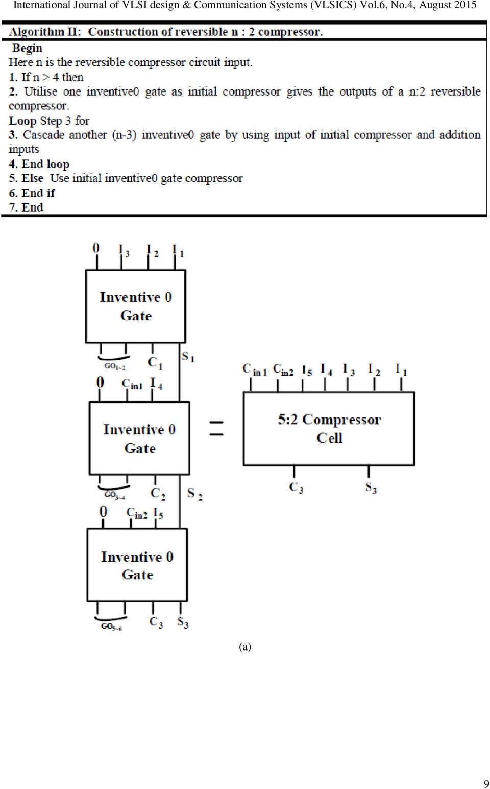
10 (b) Figure 7. Proposed design of 5:2 reversible compressor. (a) Block diagram representation. (b) The proposed Quantum realization Figure 8. Design of n:2 reversible compressor 10
 The proposed Quantum realization Figure")
11 Lemma 1: A reversible n:2 compressor can be realised with (n-2) gates, where n is the input of compressor. Proof: A 4:2 compressor consist of two inventive0 gate. Hence the total number of gates required to construct the 4:2 compressor is NOG (4:2 compressor) = NOG (2x inventive0 gate) = 2 = 1+ (4-3)= 1+ (n-3) Hence the statement holds for the base case n = 4 Assume that, the statement true for n = m, Hence, a reversible m:2 compressor requires at least (m-2) reversible gates. Lemma 2: A reversible n:2 compressor can be realised with 10(n-3) quantum cost, where n is the input of compressor. Proof: A 4:2 compressor circuit is constructed with one inventive0 gate. Hence the total quantum cost of the 4:2 compressor circuit is QC (4:2 compressor) = QC (2x inventive0 gate) = 10 = 10 (4-3) Hence the statement hold for the base case n = 4 Assume that, the statement true for n=m, Hence a reversible m:2 compressor can be realized with 10(m-3) quantum cost. Lemma 3: A reversible n:2 compressor generates at least (2n-4) garbage outputs, where n is the input of compressor. Proof: A 4:2 compressor circuit contains one inventive0 gate. Hence the total garbage outputs produce by 4:2 compressor is at least GO (4:2 compressor) = GO (2x inventive0 gate) = 4= (4 x 2-4) Hence, the statement holds for the base case n=4 Assume that, the statement true for n=m. Hence, a reversible m:2 compressor produce at least (2n-4) garbage outputs. Lemma 4: A reversible n:2 compressor can be realised with (n-2) ancilla input, where n is the input of compressor. Proof: A 4:2 compressor consist of two inventive0 gate. Hence the total ancilla input required to construct the 4:2 compressor is CI (4:2 compressor) = CI (2x inventive0 gate) = 2 = 1+ (4-3)= 1+ (n-3) Hence the statement holds for the base case n = 4 Assume that, the statement true for n = m, Hence, a reversible m:2 compressor requires at least (m-2) ancilla input. 5. PERFORMANCE EVALUATION ANALYSIS In this section, we have shown performance evaluation analysis with the help of figures and comparative tables. We implement basic reversible gate in MOS transistor count it is depicted in Figure 8. Table 4 shows that the performance of our 4:2 compressor circuit is better compared to existing designs. 11
 quantum cost, where n is the input of compressor. Proof: A 4:2 compressor circuit is constructed with one inventive0 gate.")
12 Figure 9. Number of MOS transistor count in different reversible gate Table 4. Comparative analysis table of 4:2 compressor 6. CONCLUSIONS In this manuscript there are two main parts; the first part deals with implementing basic reversible gates CNOT, FG, TG, PG, BJN and URG gate in MOS transistor using Gate diffusion input (GDI) technique. The MOS transistor for basic reversible gate are designed by keeping in mind for the minimum MOS transistor count and also reducing the critical path. In addition, it shows a comparative performance table to the realization of the MOS transistor count. However, in the second part, we propose 4:2 compressor and 5:2 compressor circuits using inventive0 gate and also its quantum circuits. These designs are the most effective among all other existing design in terms of gate count, garbage outputs and quantum cost. Since compressor can be used in low power VLSI circuit for reducing the impact of carry (Generated from full adder operation) of arithmetic frame design, This compressor structure will be definitely used in low power circuit, ALU, quantum computers etc. 12

13 REFERENCES [1] R.Landauer, (1961) Irreversibility and Heat Generation in the Computational Process, IBM Journal of Research and Development, pp [2] C H Bennett,(1973) Logical Reversibility of Computation, IBM Journal of Research and Development, vol. 17, no. 6, pp [3] Soghra shoaei, Majid Haghparast, (2014) Novel designs of nanometric parity preserving reversible compressor, Quantum information process, vol 13,issue 8, pp [4] Majid Haghparast, Majid Mohammadi, (2010) Novel quantum compressor designs using new genetic algorithm based simulator, analyzer and synthesizer software in nanotechnology. International Journal of Quantum Information. 8, pp [5] Neeraj Kumar Misra, Subodh Wairya, Vinod Kumar Singh, (2014) An Inventive Design of 4*4 Bit Reversible NS Gate IEEE International Conference on Recent Advances and Innovation in Engineering (ICRAIE-2014), pp [6] Sajib Kumar Mitra and Ahsan Raja Chowdhury, (2012) Minimum cost fault tolerant adder circuits in reversible logic synthesis, 25th Int. Conf. VLSI Design, VLSID, pp [7] Hafiz Md. Hasan Babu, Nazir Saleheen, Lafifa Jamal, Sheikh Muhammad Sarwar,Tsutomu Sasao (2014) "Approach to design a compact reversible low power binary comparator" IET Computers & Digital Techniques" Vol. 8, Iss. 3, pp [8] Neeraj Kumar Misra, Subodh Wairya and Vinod Kumar Singh, (2015) "Approaches to Design Feasible Error Control Scheme Based on Reversible Series Gates", European Journal of Scientific Research vol. 129, No. 3, pp [9] Neeraj Kumar Misra, Mukesh Kumar Kushwaha, Subodh Wairya and Amit Kumar, (2015) Cost Efficient Design of Reversible Adder Circuits for Low Power Applications, International Journal of Computer Applications, 117(19), pp [10] S. Islam, M. M. Rahman, Z. Begum and M. Z. Hafiz, (2010) Realization of a novel fault tolerant reversible full adder circuit in nanotechnology, The International. Arab J. Inform. Technol.7, pp [11] Neeraj Kumar Misra, Subodh Wairya and Vinod Kumar Singh, (2014) "EVOLUTION OF STRUCTURE OF SOME BINARY GROUP-BASED NBit COMPARATOR, NTo-2 N DECODER BY REVERSIBLE TECHNIQUE, N-TO-2N DECODER BY REVERSIBLE TECHNIQUE" International Journal of VLSI design & Communication Systems (VLSICS), Vol.5,No. 5: pp [12] Majid Haghparast and Keivan Navi, (2008) A novel fault tolerant reversible gate for nanotechnology based systems, American Journal of Applied Sciences. 5, pp [13] Neeraj Kumar Misra, Subodh Wairya, Vinod Kumar Singh, (2014) Preternatural Low-Power Reversible Decoder Design in 90 nm Technology Node International Journal of Scientific & Engineering Research, Volume 5, Issue 6, pp [14] J. W. Bruce, M. A. Thornton, L. Shivakumaraiah, P. S. Kokate, and X. Li, (2002) Efficient adder circuits based on a conservative reversible logic gate, in Proceedings of IEEE Symposium on VLSI, pp [15] Majid Haghparast, Soghra Shoaci, (2015) Design of a New Parity Preserving Reversible Full adder, Journal of Circuits Systems and Computers, world scientific, vol 24, no. 1, pp: [16] SubodhWairya, Rajendra Kumar Nagaria, Sudarshan Tiwari, (2012) Performance Analysis of High Speed Hybrid CMOS Full Adder Circuits for Low Voltage VLSI Design, Hindawi Publishing Corporation VLSI Design. [17] Bibhash Sen, AyushRajoria and BiplabK.Sikdar, (2013) "Design of Efficient Full adder in Quantum-Dot cellular Automata" The scientific World Journal Hindawi Publishing Corporation, pp [18] Pallavi devi gopineedi, Himanshu Thapliyal, M.B Srinivas and Hamid R. Arabnia,(2006) Novel and Efficient 4:2 and 5:2 compressor with minimum number of transistor designed for low power operation In ESA, pp [19] Bibhash Sen, Siddhant Ganeriwal and Biplab K. Sikdar, (2013) Reversible Logic-Based Fault-Tolerant Nanocircuits in QCA, ISRN Electronics Hindawi Publishing Corporation. [20] Adarsh Kumar Agrawal, S.Wairya, R.K. Nagaria and S.Tiwari, (2009) "A New Mixed Gate Diffusio Input Adder Topology for High Speed Low Power Digital Circuits, World Applied Sciences Journal, pp [21] Neeraj Mishra, and Asmita Haveliya, (2013) "An advancement in the N N Multiplier Architecture Realization via the Ancient Indian Vedic Mathematics." IJECCE 4, no. 2 pp [22] Chip-Hong Chang, Jiangmin Gu, and Mingyan Zhang, (2004), "Ultra low-voltage low-power CMOS 4-2 and 5-2 compressors for fast arithmetic circuits." Circuits and Systems I: Regular Papers, IEEE Transactions on 51, no. 10, pp:
![[3] Soghra shoaei, Majid Haghparast, (2014) Novel designs of nanometric parity preserving reversible compressor, Quantum information process, vol 13,issue 8, pp. 1701-1714.](/docs-images/47/21050277/images/page_13.jpg "[4] Majid Haghparast, Majid Mohammadi, (2010) Novel quantum compressor designs using new genetic algorithm based simulator, analyzer and synthesizer software in nanotechnology.")
A New Reversible TSG Gate and Its Application For Designing Efficient Adder Circuits
 A New Reversible TSG Gate and Its Application For Designing Efficient Adder s Himanshu Thapliyal Center for VLSI and Embedded System Technologies International Institute of Information Technology Hyderabad-500019,
AN IMPROVED DESIGN OF REVERSIBLE BINARY TO BINARY CODED DECIMAL CONVERTER FOR BINARY CODED DECIMAL MULTIPLICATION
 American Journal of Applied Sciences 11 (1): 69-73, 2014 ISSN: 1546-9239 2014 Science Publication doi:10.3844/ajassp.2014.69.73 Published Online 11 (1) 2014 (http://www.thescipub.com/ajas.toc) AN IMPROVED
An Extension to DNA Based Fredkin Gate Circuits: Design of Reversible Sequential Circuits using Fredkin Gates
 An Extension to DNA Based Fredkin Gate Circuits: Design of Reversible Sequential Circuits using Fredkin Gates Himanshu Thapliyal and M.B Srinivas (thapliyalhimanshu@yahoo.com, srinivas@iiit.net) Center
A Beginning in the Reversible Logic Synthesis of Sequential Circuits
 A Beginning in the Reversible Logic Synthesis of Sequential s Himanshu Thapliyal and M.B Srinivas Centre for VLSI and Embedded System Technologies International Institute of Information Technology, Hyderabad,
COMPARATIVE ANALYSIS OF 4-BIT AND 8-BIT REVERSIBLE BARREL SHIFTER DESIGNS USING REVKIT
 COMPARATIVE ANALYSIS OF 4-BIT AND 8-BIT REVERSIBLE BARREL SHIFTER DESIGNS USING REVKIT Hariprasad R. 1, Ganesh R. 1, Ravi S. 2, Marimuthu R. 1 and Balamurugan S. 1 1 School of Electrical Engineering, VIT
International Journal of Electronics and Computer Science Engineering 1482
 International Journal of Electronics and Computer Science Engineering 1482 Available Online at www.ijecse.org ISSN- 2277-1956 Behavioral Analysis of Different ALU Architectures G.V.V.S.R.Krishna Assistant
A Novel Low Power Fault Tolerant Full Adder for Deep Submicron Technology
 International Journal of Computer Sciences and Engineering Open Access Research Paper Volume-4, Issue-1 E-ISSN: 2347-2693 A Novel Low Power Fault Tolerant Full Adder for Deep Submicron Technology Zahra
NEW adder cells are useful for designing larger circuits despite increase in transistor count by four per cell.
 CHAPTER 4 THE ADDER The adder is one of the most critical components of a processor, as it is used in the Arithmetic Logic Unit (ALU), in the floating-point unit and for address generation in case of cache
Design of Low Power One-Bit Hybrid-CMOS Full Adder Cells
 Design of Low Power One-Bit Hybrid-CMOS Full Adder Cells Sushil B. Bhaisare 1, Sonalee P. Suryawanshi 2, Sagar P. Soitkar 3 1 Lecturer in Electronics Department, Nagpur University, G.H.R.I.E.T.W. Nagpur,
A New Low Power Dynamic Full Adder Cell Based on Majority Function
 World Applied Sciences Journal 4 (1): 133-141, 2008 ISSN 1818-4952 IDOSI Publications, 2008 A New Low Power Dynamic Full Adder Cell Based on Majority Function 1 Vahid Foroutan, 2 Keivan Navi and 1 Majid
High Speed Gate Level Synchronous Full Adder Designs
 High Speed Gate Level Synchronous Full Adder Designs PADMANABHAN BALASUBRAMANIAN and NIKOS E. MASTORAKIS School of Computer Science, The University of Manchester, Oxford Road, Manchester M13 9PL, UNITED
Keywords Quantum logic gates, Quantum computing, Logic gate, Quantum computer
 Volume 3 Issue 10 October 2013 ISSN: 2277 128X International Journal of Advanced Research in Computer Science and Software Engineering Research Paper Available online at: www.ijarcsse.com An Introduction
Sistemas Digitais I LESI - 2º ano
 Sistemas Digitais I LESI - 2º ano Lesson 6 - Combinational Design Practices Prof. João Miguel Fernandes (miguel@di.uminho.pt) Dept. Informática UNIVERSIDADE DO MINHO ESCOLA DE ENGENHARIA - PLDs (1) - The
LOW POWER MULTIPLEXER BASED FULL ADDER USING PASS TRANSISTOR LOGIC
 LOW POWER MULTIPLEXER BASED FULL ADDER USING PASS TRANSISTOR LOGIC B. Dilli kumar 1, K. Charan kumar 1, M. Bharathi 2 Abstract- The efficiency of a system mainly depends on the performance of the internal
HIGH SPEED AREA EFFICIENT 1-BIT HYBRID FULL ADDER
 HIGH SPEED AREA EFFICIENT 1-BIT HYBRID FULL ADDER Sachin Kumar *1, Aman Kumar #2, Puneet Bansal #3 * Department of Electronic Science, Kurukshetra University, Kurukshetra, Haryana, India # University Institute
Design and FPGA Implementation of a Novel Square Root Evaluator based on Vedic Mathematics
 International Journal of Information & Computation Technology. ISSN 0974-2239 Volume 4, Number 15 (2014), pp. 1531-1537 International Research Publications House http://www. irphouse.com Design and FPGA
A Novel Low Power, High Speed 14 Transistor CMOS Full Adder Cell with 50% Improvement in Threshold Loss Problem
 A Novel Low Power, High Speed 4 Transistor CMOS Full Adder Cell with 5% Improvement in Threshold Loss Problem T. Vigneswaran, B. Mukundhan, and P. Subbarami Reddy Abstract Full adders are important components
Implementation of Modified Booth Algorithm (Radix 4) and its Comparison with Booth Algorithm (Radix-2)
 and its Comparison with Booth Algorithm (Radix-2)") Advance in Electronic and Electric Engineering. ISSN 2231-1297, Volume 3, Number 6 (2013), pp. 683-690 Research India Publications http://www.ripublication.com/aeee.htm Implementation of Modified Booth
Advance in Electronic and Electric Engineering. ISSN 2231-1297, Volume 3, Number 6 (2013), pp. 683-690 Research India Publications http://www.ripublication.com/aeee.htm Implementation of Modified Booth
Floating Point Fused Add-Subtract and Fused Dot-Product Units
 Floating Point Fused Add-Subtract and Fused Dot-Product Units S. Kishor [1], S. P. Prakash [2] PG Scholar (VLSI DESIGN), Department of ECE Bannari Amman Institute of Technology, Sathyamangalam, Tamil Nadu,
High Speed and Efficient 4-Tap FIR Filter Design Using Modified ETA and Multipliers
 High Speed and Efficient 4-Tap FIR Filter Design Using Modified ETA and Multipliers Mehta Shantanu Sheetal #1, Vigneswaran T. #2 # School of Electronics Engineering, VIT University Chennai, Tamil Nadu,
A CDMA Based Scalable Hierarchical Architecture for Network- On-Chip
 www.ijcsi.org 241 A CDMA Based Scalable Hierarchical Architecture for Network- On-Chip Ahmed A. El Badry 1 and Mohamed A. Abd El Ghany 2 1 Communications Engineering Dept., German University in Cairo,
Design of Energy Efficient Low Power Full Adder using Supply Voltage Gating
 Design of Energy Efficient Low Power Full Adder using Supply Voltage Gating S.Nandhini 1, T.G.Dhaarani 2, P.Kokila 3, P.Premkumar 4 Assistant Professor, Dept. of ECE, Nandha Engineering College, Erode,
Performance Comparison of an Algorithmic Current- Mode ADC Implemented using Different Current Comparators
 Performance Comparison of an Algorithmic Current- Mode ADC Implemented using Different Current Comparators Veepsa Bhatia Indira Gandhi Delhi Technical University for Women Delhi, India Neeta Pandey Delhi
Innovative improvement of fundamental metrics including power dissipation and efficiency of the ALU system
 Innovative improvement of fundamental metrics including power dissipation and efficiency of the ALU system Joseph LaBauve Department of Electrical and Computer Engineering University of Central Florida
LOW POWER CMOS FULL ADDER DESIGN WITH 12 TRANSISTORS
 LOW POWER CMOS FULL ADDER DESIGN WITH 12 TRANSISTORS Manoj Kumar 1, Sandeep K. Arya 1, Sujata Pandey 2 1 Department of Electronics & Communication Engineering Guru Jambheshwar University of Science & Technology,
Efficient Interconnect Design with Novel Repeater Insertion for Low Power Applications
 Efficient Interconnect Design with Novel Repeater Insertion for Low Power Applications TRIPTI SHARMA, K. G. SHARMA, B. P. SINGH, NEHA ARORA Electronics & Communication Department MITS Deemed University,
Let s put together a Manual Processor
 Lecture 14 Let s put together a Manual Processor Hardware Lecture 14 Slide 1 The processor Inside every computer there is at least one processor which can take an instruction, some operands and produce
ECE410 Design Project Spring 2008 Design and Characterization of a CMOS 8-bit Microprocessor Data Path
 ECE410 Design Project Spring 2008 Design and Characterization of a CMOS 8-bit Microprocessor Data Path Project Summary This project involves the schematic and layout design of an 8-bit microprocessor data
Optimization and Comparison of 4-Stage Inverter, 2-i/p NAND Gate, 2-i/p NOR Gate Driving Standard Load By Using Logical Effort
 Optimization and Comparison of -Stage, -i/p NND Gate, -i/p NOR Gate Driving Standard Load By Using Logical Effort Satyajit nand *, and P.K.Ghosh ** * Mody Institute of Technology & Science/ECE, Lakshmangarh,
COMBINATIONAL CIRCUITS
 COMBINATIONAL CIRCUITS http://www.tutorialspoint.com/computer_logical_organization/combinational_circuits.htm Copyright tutorialspoint.com Combinational circuit is a circuit in which we combine the different
ONLINE TESTING IN TERNARY REVERSIBLE LOGIC
 ONLINE TESTING IN TERNARY REVERSIBLE LOGIC MD. RAQIBUR RAHMAN Bachelor of Science, University of Dhaka, 2004 Master of Science, University of Dhaka, 2005 A Thesis Submitted to the School of Graduate Studies
1. True or False? A voltage level in the range 0 to 2 volts is interpreted as a binary 1.
 File: chap04, Chapter 04 1. True or False? A voltage level in the range 0 to 2 volts is interpreted as a binary 1. 2. True or False? A gate is a device that accepts a single input signal and produces one
United States Naval Academy Electrical and Computer Engineering Department. EC262 Exam 1
 United States Naval Academy Electrical and Computer Engineering Department EC262 Exam 29 September 2. Do a page check now. You should have pages (cover & questions). 2. Read all problems in their entirety.
Understanding Logic Design
 Understanding Logic Design ppendix of your Textbook does not have the needed background information. This document supplements it. When you write add DD R0, R1, R2, you imagine something like this: R1
An Efficient RNS to Binary Converter Using the Moduli Set {2n + 1, 2n, 2n 1}
 An Efficient RNS to Binary Converter Using the oduli Set {n + 1, n, n 1} Kazeem Alagbe Gbolagade 1,, ember, IEEE and Sorin Dan Cotofana 1, Senior ember IEEE, 1. Computer Engineering Laboratory, Delft University
A high Speed 8 Transistor Full Adder Design using Novel 3 Transistor XOR Gates
 A high Speed 8 Transistor Full Adder Design using Novel 3 Transistor XOR Gates Shubhajit Roy Chowdhury, Aritra Banerjee, Aniruddha Roy, Hiranmay Saha Abstract The paper proposes the novel design of a 3T
e.g. τ = 12 ps in 180nm, 40 ps in 0.6 µm Delay has two components where, f = Effort Delay (stage effort)= gh p =Parasitic Delay
= gh p =Parasitic Delay") Logic Gate Delay Chip designers need to choose: What is the best circuit topology for a function? How many stages of logic produce least delay? How wide transistors should be? Logical Effort Helps make
Logic Gate Delay Chip designers need to choose: What is the best circuit topology for a function? How many stages of logic produce least delay? How wide transistors should be? Logical Effort Helps make
Digital Logic Design. Basics Combinational Circuits Sequential Circuits. Pu-Jen Cheng
 Digital Logic Design Basics Combinational Circuits Sequential Circuits Pu-Jen Cheng Adapted from the slides prepared by S. Dandamudi for the book, Fundamentals of Computer Organization and Design. Introduction
Chapter 4 Register Transfer and Microoperations. Section 4.1 Register Transfer Language
 Chapter 4 Register Transfer and Microoperations Section 4.1 Register Transfer Language Digital systems are composed of modules that are constructed from digital components, such as registers, decoders,
Chapter 2 Logic Gates and Introduction to Computer Architecture
 Chapter 2 Logic Gates and Introduction to Computer Architecture 2.1 Introduction The basic components of an Integrated Circuit (IC) is logic gates which made of transistors, in digital system there are
Static-Noise-Margin Analysis of Conventional 6T SRAM Cell at 45nm Technology
 Static-Noise-Margin Analysis of Conventional 6T SRAM Cell at 45nm Technology Nahid Rahman Department of electronics and communication FET-MITS (Deemed university), Lakshmangarh, India B. P. Singh Department
Design Verification and Test of Digital VLSI Circuits NPTEL Video Course. Module-VII Lecture-I Introduction to Digital VLSI Testing
 Design Verification and Test of Digital VLSI Circuits NPTEL Video Course Module-VII Lecture-I Introduction to Digital VLSI Testing VLSI Design, Verification and Test Flow Customer's Requirements Specifications
An Effective Deterministic BIST Scheme for Shifter/Accumulator Pairs in Datapaths
 An Effective Deterministic BIST Scheme for Shifter/Accumulator Pairs in Datapaths N. KRANITIS M. PSARAKIS D. GIZOPOULOS 2 A. PASCHALIS 3 Y. ZORIAN 4 Institute of Informatics & Telecommunications, NCSR
Vedicmultiplier for RC6 Encryption Standards Using FPGA
 Vedicmultiplier for RC6 Encryption Standards Using FPGA M. Kavitha 1, CH. Rajendra Prasad 2, Dr. Syed Musthak Ahmed 3 Department of ECE, SR Engineering College, Warangal, India 1,2,3 ABSTRACT: This paper
10 BIT s Current Mode Pipelined ADC
 10 BIT s Current Mode Pipelined ADC K.BHARANI VLSI DEPARTMENT VIT UNIVERSITY VELLORE, INDIA kothareddybharani@yahoo.com P.JAYAKRISHNAN VLSI DEPARTMENT VIT UNIVERSITY VELLORE, INDIA pjayakrishnan@vit.ac.in
LFSR BASED COUNTERS AVINASH AJANE, B.E. A technical report submitted to the Graduate School. in partial fulfillment of the requirements
 LFSR BASED COUNTERS BY AVINASH AJANE, B.E A technical report submitted to the Graduate School in partial fulfillment of the requirements for the degree Master of Science in Electrical Engineering New Mexico
Gates, Circuits, and Boolean Algebra
 Gates, Circuits, and Boolean Algebra Computers and Electricity A gate is a device that performs a basic operation on electrical signals Gates are combined into circuits to perform more complicated tasks
DEFECT ANALYSIS OF QUANTUM-DOT CELLULAR AUTOMATA COMBINATIONAL CIRCUIT USING HDLQ
 International Journal of Advanced Research in Engineering and Technology (IJARET) Volume 7, Issue 2, March-April 2016, pp. 148 158, Article ID: IJARET_07_02_014 Available online at http://www.iaeme.com/ijaret/issues.asp?jtype=ijaret&vtype=7&itype=2
Sequential 4-bit Adder Design Report
 UNIVERSITY OF WATERLOO Faculty of Engineering E&CE 438: Digital Integrated Circuits Sequential 4-bit Adder Design Report Prepared by: Ian Hung (ixxxxxx), 99XXXXXX Annette Lo (axxxxxx), 99XXXXXX Pamela
Lecture 5: Gate Logic Logic Optimization
 Lecture 5: Gate Logic Logic Optimization MAH, AEN EE271 Lecture 5 1 Overview Reading McCluskey, Logic Design Principles- or any text in boolean algebra Introduction We could design at the level of irsim
A High Speed Binary Floating Point Multiplier using Dadda Algorithm
 A High Speed Binary Floating Point Multiplier using Dadda Algorithm Prakhi Agrawal 1, Prof. Shravan Sable 2, Dr. Rita Jain 3 M-Tech Research Scholar, Department of Electronics & Communication Engineering
ON SUITABILITY OF FPGA BASED EVOLVABLE HARDWARE SYSTEMS TO INTEGRATE RECONFIGURABLE CIRCUITS WITH HOST PROCESSING UNIT
 216 ON SUITABILITY OF FPGA BASED EVOLVABLE HARDWARE SYSTEMS TO INTEGRATE RECONFIGURABLE CIRCUITS WITH HOST PROCESSING UNIT *P.Nirmalkumar, **J.Raja Paul Perinbam, @S.Ravi and #B.Rajan *Research Scholar,
FAULT TOLERANCE FOR MULTIPROCESSOR SYSTEMS VIA TIME REDUNDANT TASK SCHEDULING
 FAULT TOLERANCE FOR MULTIPROCESSOR SYSTEMS VIA TIME REDUNDANT TASK SCHEDULING Hussain Al-Asaad and Alireza Sarvi Department of Electrical & Computer Engineering University of California Davis, CA, U.S.A.
INTEGRATED CIRCUITS. For a complete data sheet, please also download:
 INTEGRATED CIRCUITS DATA SHEET For a complete data sheet, please also download: The IC06 74HC/HCT/HCU/HCMOS Logic Family Specifications The IC06 74HC/HCT/HCU/HCMOS Logic Package Information The IC06 74HC/HCT/HCU/HCMOS
CHAPTER 3 Boolean Algebra and Digital Logic
 CHAPTER 3 Boolean Algebra and Digital Logic 3.1 Introduction 121 3.2 Boolean Algebra 122 3.2.1 Boolean Expressions 123 3.2.2 Boolean Identities 124 3.2.3 Simplification of Boolean Expressions 126 3.2.4
How To Fix A 3 Bit Error In Data From A Data Point To A Bit Code (Data Point) With A Power Source (Data Source) And A Power Cell (Power Source)
 With A Power Source (Data Source) And A Power Cell (Power Source)") FPGA IMPLEMENTATION OF 4D-PARITY BASED DATA CODING TECHNIQUE Vijay Tawar 1, Rajani Gupta 2 1 Student, KNPCST, Hoshangabad Road, Misrod, Bhopal, Pin no.462047 2 Head of Department (EC), KNPCST, Hoshangabad
FPGA IMPLEMENTATION OF 4D-PARITY BASED DATA CODING TECHNIQUE Vijay Tawar 1, Rajani Gupta 2 1 Student, KNPCST, Hoshangabad Road, Misrod, Bhopal, Pin no.462047 2 Head of Department (EC), KNPCST, Hoshangabad
Gates. J. Robert Jump Department of Electrical And Computer Engineering Rice University Houston, TX 77251
 Gates J. Robert Jump Department of Electrical And Computer Engineering Rice University Houston, T 77251 1. The Evolution of Electronic Digital Devices...1 2. Logical Operations and the Behavior of Gates...2
Systems I: Computer Organization and Architecture
 Systems I: Computer Organization and Architecture Lecture 9 - Register Transfer and Microoperations Microoperations Digital systems are modular in nature, with modules containing registers, decoders, arithmetic
A MULTILEVEL INVERTER FOR SYNCHRONIZING THE GRID WITH RENEWABLE ENERGY SOURCES BY IMPLEMENTING BATTERY CUM DC-DC CONERTER
 A MULTILEVEL INVERTER FOR SYNCHRONIZING THE GRID WITH RENEWABLE ENERGY SOURCES BY IMPLEMENTING BATTERY CUM DC-DC CONERTER 1 KARUNYA CHRISTOBAL LYDIA. S, 2 SHANMUGASUNDARI. A, 3 ANANDHI.Y 1,2,3 Electrical
Implementation of Reliable Fault Tolerant Data Storage System over Cloud using Raid 60
 International Journal of Computer Sciences and Engineering Open Access Review Paper Volume-4, Issue-2 E-ISSN: 2347-2693 Implementation of Reliable Fault Tolerant Data Storage System over Cloud using Raid
exclusive-or and Binary Adder R eouven Elbaz reouven@uwaterloo.ca Office room: DC3576
 exclusive-or and Binary Adder R eouven Elbaz reouven@uwaterloo.ca Office room: DC3576 Outline exclusive OR gate (XOR) Definition Properties Examples of Applications Odd Function Parity Generation and Checking
Binary Adders: Half Adders and Full Adders
 Binary Adders: Half Adders and Full Adders In this set of slides, we present the two basic types of adders: 1. Half adders, and 2. Full adders. Each type of adder functions to add two binary bits. In order
ISSN: 2319-5967 ISO 9001:2008 Certified International Journal of Engineering Science and Innovative Technology (IJESIT) Volume 2, Issue 3, May 2013
 Volume 2, Issue 3, May 2013") Transistor Level Fault Finding in VLSI Circuits using Genetic Algorithm Lalit A. Patel, Sarman K. Hadia CSPIT, CHARUSAT, Changa., CSPIT, CHARUSAT, Changa Abstract This paper presents, genetic based algorithm
Transistor Level Fault Finding in VLSI Circuits using Genetic Algorithm Lalit A. Patel, Sarman K. Hadia CSPIT, CHARUSAT, Changa., CSPIT, CHARUSAT, Changa Abstract This paper presents, genetic based algorithm
An Open Architecture through Nanocomputing
 2009 International Symposium on Computing, Communication, and Control (ISCCC 2009) Proc.of CSIT vol.1 (2011) (2011) IACSIT Press, Singapore An Open Architecture through Nanocomputing Joby Joseph1and A.
CSE140 Homework #7 - Solution
 CSE140 Spring2013 CSE140 Homework #7 - Solution You must SHOW ALL STEPS for obtaining the solution. Reporting the correct answer, without showing the work performed at each step will result in getting
Implementation and Design of AES S-Box on FPGA
 International Journal of Research in Engineering and Science (IJRES) ISSN (Online): 232-9364, ISSN (Print): 232-9356 Volume 3 Issue ǁ Jan. 25 ǁ PP.9-4 Implementation and Design of AES S-Box on FPGA Chandrasekhar
Hardware Implementation of AES Encryption and Decryption System Based on FPGA
 Send Orders for Reprints to reprints@benthamscience.ae The Open Cybernetics & Systemics Journal, 2015, 9, 1373-1377 1373 Open Access Hardware Implementation of AES Encryption and Decryption System Based
Here we introduced (1) basic circuit for logic and (2)recent nano-devices, and presented (3) some practical issues on nano-devices.
 basic circuit for logic and (2)recent nano-devices, and presented (3) some practical issues on nano-devices.") Outline Here we introduced () basic circuit for logic and (2)recent nano-devices, and presented (3) some practical issues on nano-devices. Circuit Logic Gate A logic gate is an elemantary building block
Outline Here we introduced () basic circuit for logic and (2)recent nano-devices, and presented (3) some practical issues on nano-devices. Circuit Logic Gate A logic gate is an elemantary building block
Design and analysis of flip flops for low power clocking system
 Design and analysis of flip flops for low power clocking system Gabariyala sabadini.c PG Scholar, VLSI design, Department of ECE,PSNA college of Engg and Tech, Dindigul,India. Jeya priyanka.p PG Scholar,
Introduction to computer science
 Introduction to computer science Michael A. Nielsen University of Queensland Goals: 1. Introduce the notion of the computational complexity of a problem, and define the major computational complexity classes.
Verification & Design Techniques Used in a Graduate Level VHDL Course
 Verification & Design Techniques Used in a Graduate Level VHDL Course Prof. Swati Agrawal, BE, MS (SUNY, Buffalo, NY USA) 1 Associate Professor, Department of Electronics & Telecommunication, Bhilai Institute
Lab 1: Full Adder 0.0
 Lab 1: Full Adder 0.0 Introduction In this lab you will design a simple digital circuit called a full adder. You will then use logic gates to draw a schematic for the circuit. Finally, you will verify
Multipliers. Introduction
 Multipliers Introduction Multipliers play an important role in today s digital signal processing and various other applications. With advances in technology, many researchers have tried and are trying
Design Methods for Binary to Decimal Converters Using Arithmetic Decompositions
 J. of Mult.-Valued Logic & Soft Computing, Vol., pp. 8 7 Old City Publishing, Inc. Reprints available directly from the publisher Published by license under the OCP Science imprint, Photocopying permitted
Digital Electronics Detailed Outline
 Digital Electronics Detailed Outline Unit 1: Fundamentals of Analog and Digital Electronics (32 Total Days) Lesson 1.1: Foundations and the Board Game Counter (9 days) 1. Safety is an important concept
Analog & Digital Electronics Course No: PH-218
 Analog & Digital Electronics Course No: PH-218 Lec-28: Logic Gates & Family Course Instructor: Dr. A. P. VAJPEYI Department of Physics, Indian Institute of Technology Guwahati, India 1 Digital Logic Gates
A PERFORMANCE EVALUATION OF COMMON ENCRYPTION TECHNIQUES WITH SECURE WATERMARK SYSTEM (SWS)
") A PERFORMANCE EVALUATION OF COMMON ENCRYPTION TECHNIQUES WITH SECURE WATERMARK SYSTEM (SWS) Ashraf Odeh 1, Shadi R.Masadeh 2, Ahmad Azzazi 3 1 Computer Information Systems Department, Isra University,
A PERFORMANCE EVALUATION OF COMMON ENCRYPTION TECHNIQUES WITH SECURE WATERMARK SYSTEM (SWS) Ashraf Odeh 1, Shadi R.Masadeh 2, Ahmad Azzazi 3 1 Computer Information Systems Department, Isra University,
The concept of hierarchical design: the views of computer science and engineering students
 The concept of hierarchical design: the views of computer science and engineering students Lambrini Adamopoulou, Maria Kordaki and George Alexiou Department of Computer Engineering and Informatics, Patras
Gate Delay Model. Estimating Delays. Effort Delay. Gate Delay. Computing Logical Effort. Logical Effort
 Estimating Delays Would be nice to have a back of the envelope method for sizing gates for speed Logical Effort Book by Sutherland, Sproull, Harris Chapter 1 is on our web page Also Chapter 4 in our textbook
ANALOG & DIGITAL ELECTRONICS
 ANALOG & DIGITAL ELECTRONICS Course Instructor: Course No: PH-218 3-1-0-8 Dr. A.P. Vajpeyi E-mail: apvajpeyi@iitg.ernet.in Room No: #305 Department of Physics, Indian Institute of Technology Guwahati,
Adder.PPT(10/1/2009) 5.1. Lecture 13. Adder Circuits
 5.1. Lecture 13. Adder Circuits") Adder.T(//29) 5. Lecture 3 Adder ircuits Objectives Understand how to add both signed and unsigned numbers Appreciate how the delay of an adder circuit depends on the data values that are being added together
Adder.T(//29) 5. Lecture 3 Adder ircuits Objectives Understand how to add both signed and unsigned numbers Appreciate how the delay of an adder circuit depends on the data values that are being added together
Error Detection and Data Recovery Architecture for Systolic Motion Estimators
 Error Detection and Data Recovery Architecture for Systolic Motion Estimators L. Arun Kumar #1, L. Sheela *2 # PG Scholar, * Assistant Professor, Embedded System Technologies, Regional Center of Anna University
TRUE SINGLE PHASE CLOCKING BASED FLIP-FLOP DESIGN
 TRUE SINGLE PHASE CLOCKING BASED FLIP-FLOP DESIGN USING DIFFERENT FOUNDRIES Priyanka Sharma 1 and Rajesh Mehra 2 1 ME student, Department of E.C.E, NITTTR, Chandigarh, India 2 Associate Professor, Department
A Parallel Processor for Distributed Genetic Algorithm with Redundant Binary Number
 A Parallel Processor for Distributed Genetic Algorithm with Redundant Binary Number 1 Tomohiro KAMIMURA, 2 Akinori KANASUGI 1 Department of Electronics, Tokyo Denki University, 07ee055@ms.dendai.ac.jp
ISSCC 2003 / SESSION 13 / 40Gb/s COMMUNICATION ICS / PAPER 13.7
 ISSCC 2003 / SESSION 13 / 40Gb/s COMMUNICATION ICS / PAPER 13.7 13.7 A 40Gb/s Clock and Data Recovery Circuit in 0.18µm CMOS Technology Jri Lee, Behzad Razavi University of California, Los Angeles, CA
Flip-Flops, Registers, Counters, and a Simple Processor
 June 8, 22 5:56 vra235_ch7 Sheet number Page number 349 black chapter 7 Flip-Flops, Registers, Counters, and a Simple Processor 7. Ng f3, h7 h6 349 June 8, 22 5:56 vra235_ch7 Sheet number 2 Page number
A Novel Switch Mechanism for Load Balancing in Public Cloud
 International OPEN ACCESS Journal Of Modern Engineering Research (IJMER) A Novel Switch Mechanism for Load Balancing in Public Cloud Kalathoti Rambabu 1, M. Chandra Sekhar 2 1 M. Tech (CSE), MVR College
CMOS Binary Full Adder
 CMOS Binary Full Adder A Survey of Possible Implementations Group : Eren Turgay Aaron Daniels Michael Bacelieri William Berry - - Table of Contents Key Terminology...- - Introduction...- 3 - Design Architectures...-
Combinational Logic Design
 Chapter 4 Combinational Logic Design The foundations for the design of digital logic circuits were established in the preceding chapters. The elements of Boolean algebra (two-element switching algebra
Design of Reversible Random Access Memory
 International Journal of omputer pplications (975 8887) Volume 56 No.15, October 212 esign of Reversible Random ccess Memory Md. Selim l Mamun epartment of omputer Science and Engineering, Jatiya Kabi
2695 P a g e. IV Semester M.Tech (DCN) SJCIT Chickballapur Karnataka India
 SJCIT Chickballapur Karnataka India") Integrity Preservation and Privacy Protection for Digital Medical Images M.Krishna Rani Dr.S.Bhargavi IV Semester M.Tech (DCN) SJCIT Chickballapur Karnataka India Abstract- In medical treatments, the integrity
Integrity Preservation and Privacy Protection for Digital Medical Images M.Krishna Rani Dr.S.Bhargavi IV Semester M.Tech (DCN) SJCIT Chickballapur Karnataka India Abstract- In medical treatments, the integrity
Gates & Boolean Algebra. Boolean Operators. Combinational Logic. Introduction
 Introduction Gates & Boolean lgebra Boolean algebra: named after mathematician George Boole (85 864). 2-valued algebra. digital circuit can have one of 2 values. Signal between and volt =, between 4 and
Parametric variation analysis of CUK converter for constant voltage applications
 ISSN (Print) : 232 3765 (An ISO 3297: 27 Certified Organization) Vol. 3, Issue 2, February 214 Parametric variation analysis of CUK converter for constant voltage applications Rheesabh Dwivedi 1, Vinay
earlier in the semester: The Full adder above adds two bits and the output is at the end. So if we do this eight times, we would have an 8-bit adder.
 The circuit created is an 8-bit adder. The 8-bit adder adds two 8-bit binary inputs and the result is produced in the output. In order to create a Full 8-bit adder, I could use eight Full -bit adders and
Load Balancing in Fault Tolerant Video Server
 Load Balancing in Fault Tolerant Video Server # D. N. Sujatha*, Girish K*, Rashmi B*, Venugopal K. R*, L. M. Patnaik** *Department of Computer Science and Engineering University Visvesvaraya College of
A Hybrid Electrical and Optical Networking Topology of Data Center for Big Data Network
 ASEE 2014 Zone I Conference, April 3-5, 2014, University of Bridgeport, Bridgpeort, CT, USA A Hybrid Electrical and Optical Networking Topology of Data Center for Big Data Network Mohammad Naimur Rahman
DESIGN OF AN ERROR DETECTION AND DATA RECOVERY ARCHITECTURE FOR MOTION ESTIMATION TESTING APPLICATIONS
 DESIGN OF AN ERROR DETECTION AND DATA RECOVERY ARCHITECTURE FOR MOTION ESTIMATION TESTING APPLICATIONS V. SWARNA LATHA 1 & K. SRINIVASA RAO 2 1 VLSI System Design A.I.T.S, Rajampet Kadapa (Dt), A.P., India
RN-Codings: New Insights and Some Applications
 RN-Codings: New Insights and Some Applications Abstract During any composite computation there is a constant need for rounding intermediate results before they can participate in further processing. Recently
Index Terms Domain name, Firewall, Packet, Phishing, URL.
 BDD for Implementation of Packet Filter Firewall and Detecting Phishing Websites Naresh Shende Vidyalankar Institute of Technology Prof. S. K. Shinde Lokmanya Tilak College of Engineering Abstract Packet
Lecture 8: Synchronous Digital Systems
 Lecture 8: Synchronous Digital Systems The distinguishing feature of a synchronous digital system is that the circuit only changes in response to a system clock. For example, consider the edge triggered