TOSHIBA CCD LINEAR IMAGE SENSOR CCD(Charge Coupled Device) TCD1304AP
|
|
|
- Jeffery Robbins
- 9 years ago
- Views:
Transcription
1 TOSHIBA CCD LINEAR IMAGE SENSOR CCD(Charge Coupled Device) TCD1304AP TCD1304AP The TCD1304AP is a high sensitive and low dark current 3648 elements linear image sensor. The sensor can be used for POS scanner. The device consist of sensitivity CCD chip. The TCD1304AP has electronic shutter function (ICG). Electronic shutter funtion can keep always output voltage constant that vary with intensity of lights. FEATURES Pixel Number : 3648 Pixel Size : 8µm 200µm Photo Sensing Region : High Sensitive & Low Dark Current pn Photodiode Weight: 2.7g (Typ.) Internal Circuit : CCD Drive Circuit Power Supply : Only 3.0V Drive (MIN.) Function : Electronic Shutter Sample and Hold Circuit Package : 22 Pin DIP (T CAPP) TOSHIBA CCD ADVANCED PLASTIC PACKAGE PIN CONNECTION MAXIMUM RATINGS (Note 1) CHARACTERISTIC SYMBOL RATING UNIT Master Clock Pulse Voltage V φm SH Pulse Voltage V SH ICG Pulse Voltage V ICG 0.3~7 V Digital Power Supply V DD Analog Power Supply V AD Operating Temperature T opr 25~60 C Storage Temperature T stg 40~100 C Note: All voltage are with respect to SS terminals. (Ground) (TOP VIEW) 1

2 CIRCUIT DIAGRAM PIN NAMES φm SH ICG V AD V DD SS NC Master Clock Shift Gate Integration Clear Gate Power (Analog) Power (Digital) Ground Non Connection 2
 Ground Non Connection")
3 OPTICAL / ELECTRICAL CHARACTERISTICS (Ta = 25 C, V φ = 4.0V (PULSE), f φ = 0.5MHz, t INT (INTEGRATION TIME) = 10ms, LOAD RESISTANCE = 100kΩ, V AD = V DD = 4.0V, LIGHT SOURCE = DAYLIGHT FLUORESCENT LAMP) CHARACTERISTIC SYMBOL MIN TYP. MAX UNIT NOTE Sensitivity R V / lx s Photo Response Non Uniformity PRNU 10 % (Note 2) Register Imbalance RI 3 % (Note 3) Saturation Output Voltage V SAT mv V OD = 3.0V (Note 4) Dark Signal Voltage V MDK 2 5 mv (Note 5) Total Transfer Effeiciency TTE % Dynamic Range DR 300 (Note 6) Saturation Exposure SE lx s (Note 7) DC Power Dissipation PD mw DC Signal Output Voltage V OS V (Note 8) Output Impedance Z o kω Image Lag of Electronic Shutter VLAGICG 10 mv Tint=100µs Note 2: Measured at 50% of SE (Typ.),? Definition of PRNU: PRNU = 100 %? Where? is average of total signal outputs and,? is the maximum deviation from? under uniform illumination. Note 3: Measured at 50% of SE (Typ.) RI is defined as follows: 3647? n? n 1 RI = n % 3647? Where? n and? n+1 are signal outputs of each pixel.? is average of total signal outputs. Note 4: V SAT is defined as minimum saturation output voltage of all effective pixels. Note 5: V MDK is defined as maximum dark signal voltage of all effective pixels. 3
 Dark Signal Voltage V MDK 2 5 mv (Note 5) Total Transfer Effeiciency TTE 92 95 % Dynamic Range DR 300 (Note 6) Saturation Exposure SE 0.")
4 Note 6: Definition of DR : DR = VSAT VMDK V MDK is proportional to t INT (Integration time). So the shorter t INT condition makes wider DR value. V Note 7: Definition of SE : SE = SAT lx s R Note 8: DC signal output voltage is defined as follows:. 4

5 OPERATING CONDITION CHARACTERISTIC SYMBOL MIN TYP. MAX UNIT Master Clock Pulse Voltage H Level V φm V L Level SH Pulse Voltage H Level V SH V L Level ICG Pulse Voltage H Level V ICG V L Level Digital Power Supply V DD V Analog Power Supply V AD V Note: V AD = V DD MAX. Voltage of Pulse Voltage H Level = V DD MIN. Voltage of Pulse Voltage H Level = V DD 0.5V CLOCK CHARACTERISTICS (Ta = 25 C) (V AD = V DD 4.0V) CHARACTERISTIC SYMBOL MIN TYP. MAX UNIT Master Clock Frequency f φm MHz Data Rate f DATA MHz Master Clock Capacitance C φm 10 pf Shift Pulse Capacitance C SH 600 pf ICG Pulse Capacitance C ICG 250 pf CLOCK CHARACTERISTICS (Ta = 25 C) (4.0V>V AD = V DD 3.0V) CHARACTERISTIC SYMBOL MIN TYP. MAX UNIT Master Clock Frequency f φm MHz Data Rate f DATA MHz 5
 (4.0V>V AD = V DD 3.")
6 TIMING CHART TCD1304AP 6 6

7 TIMING CHART (Use electric shutter function) 7 TCD1304AP 7 TCD1304AP
 7")
8 TIMING REQUIREMENTS CHARACTERISTIC SYMBOL MIN TYP. MAX UNIT ICG Pulse DELAY t ns Pulse Timing of ICG and S H t ns SH Pulse Width t ns Pulse Timing of ICG and φ M t * ns *: You keep φ M High Level. Note: If you use electronic shutter function. t INT (MIN.) = 10µs 8

9 USE ELECTRONIC SHUTTER Pulse Timing of SH and ICG SH cycle = Tint t INT (MIN.) = 10µs You have always same SH pulse width (t3). 9
 = 10µs You have always same SH")
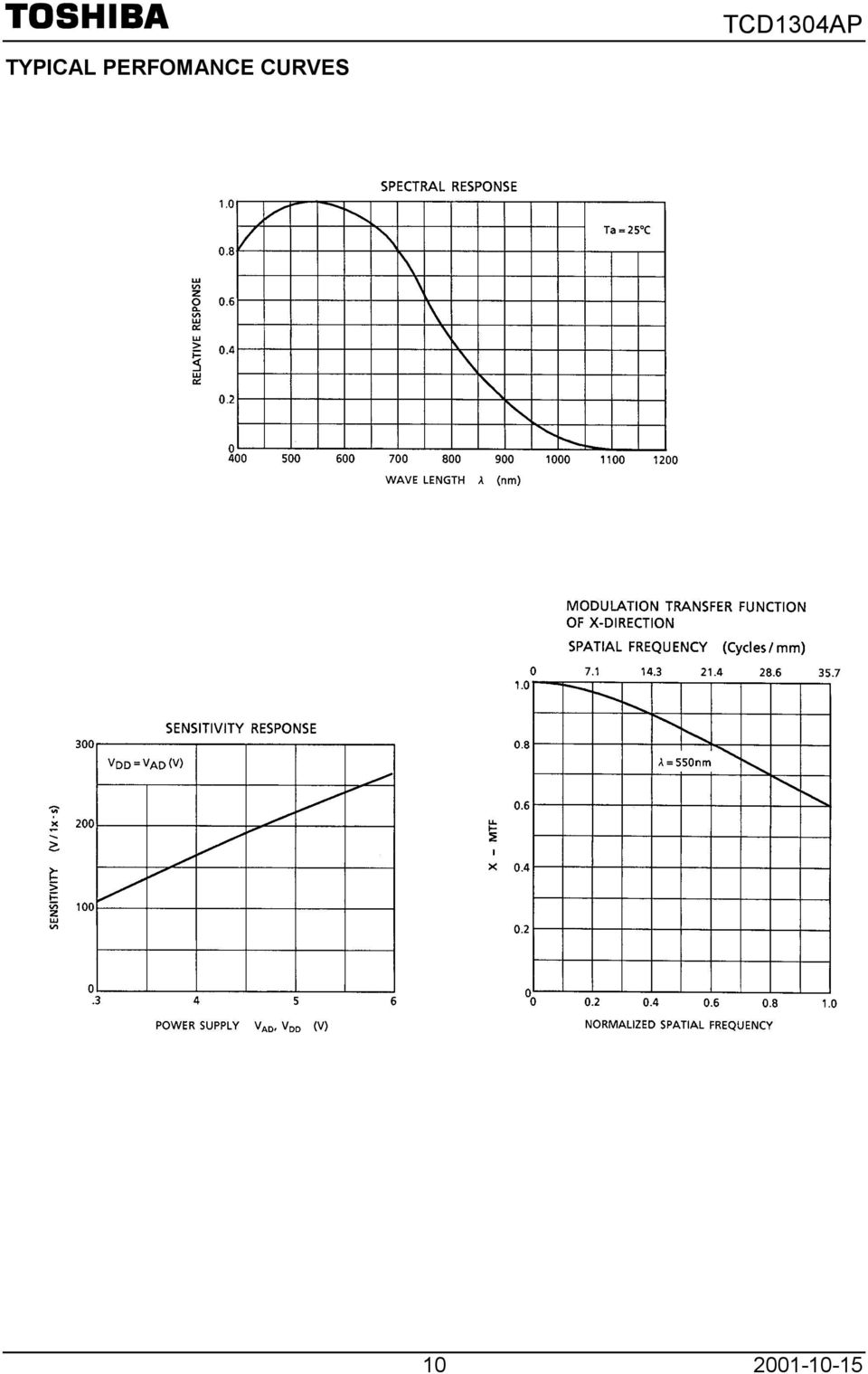
10 TYPICAL PERFOMANCE CURVES 10
11 TYPICAL PERFOMANCE CURVES 11

12 TYPICAL DRIVE CIRCUIT 12

13 CAUTION 1. Window Glass The dust and stain on the glass window of the package degrade optical performance of CCD sensor. Keep the glass window clean by saturating a cotton swab in alcohol and lightly wiping the surface, and allow the glass to dry, by blowing with filtered dry N2. Care should be taken to avoid mechanical or thermal shock because the glass window is easily to damage. 2. Electrostatic Breakdown Store in shorting clip or in conductive foam to avoid electrostatic breakdown. CCD Image Sensor is protected against static electricity, but interior puncture mode device due to static electricity is sometimes detected. In handing the device, it is necessary to execute the following static electricity preventive measures, in order to prevent the trouble rate increase of the manufacturing system due to static electricity. a. Prevent the generation of static electricity due to friction by making the work with bare hands or by putting on cotton gloves and non-charging working clothes. b. Discharge the static electricity by providing earth plate or earth wire on the floor, door or stand of the work room. c. Ground the tools such as soldering iron, radio cutting pliers of or pincer. It is not necessarily required to execute all precaution items for static electricity. It is all right to mitigate the precautions by confirming that the trouble rate within the prescribed range. 3. Incident Light CCD sensor is sensitive to infrared light. Note that infrared light component degrades resolution and PRNU of CCD sensor. 4. Lead Frame Forming Since this package is not strong against mechanical stress, you should not reform the lead frame. We recommend to use a IC-inserter when you assemble to PCB. 5. Soldering Soldering by the solder flow method cannot be guaranteed because this method may have deleterious effects on prevention of window glass soiling and heat resistance. Using a soldering iron, complete soldering within ten seconds for lead temperatures of up to 260 C, or within three seconds for lead temperatures of up to 350 C. 13

14 PACKAGE DIMENSIONS Unit : mm Note 1: No. 1 SENSOR ELEMENT (S1) TO EDGE OF PACKAGE. Note 2: TOP OF CHIP TO BOTTOM OF PACKAGE. Note 3: GLASS THICKNES (n = 1.5) Weight: 2.7g (Typ.) 14
 Weight: 2.")
15 RESTRICTIONS ON PRODUCT USE EBA TOSHIBA is continually working to improve the quality and reliability of its products. Nevertheless, semiconductor devices in general can malfunction or fail due to their inherent electrical sensitivity and vulnerability to physical stress. It is the responsibility of the buyer, when utilizing TOSHIBA products, to comply with the standards of safety in making a safe design for the entire system, and to avoid situations in which a malfunction or failure of such TOSHIBA products could cause loss of human life, bodily injury or damage to property. In developing your designs, please ensure that TOSHIBA products are used within specified operating ranges as set forth in the most recent TOSHIBA products specifications. Also, please keep in mind the precautions and conditions set forth in the Handling Guide for Semiconductor Devices, or TOSHIBA Semiconductor Reliability Handbook etc.. The TOSHIBA products listed in this document are intended for usage in general electronics applications (computer, personal equipment, office equipment, measuring equipment, industrial robotics, domestic appliances, etc.). These TOSHIBA products are neither intended nor warranted for usage in equipment that requires extraordinarily high quality and/or reliability or a malfunction or failure of which may cause loss of human life or bodily injury ( Unintended Usage ). Unintended Usage include atomic energy control instruments, airplane or spaceship instruments, transportation instruments, traffic signal instruments, combustion control instruments, medical instruments, all types of safety devices, etc.. Unintended Usage of TOSHIBA products listed in this document shall be made at the customer s own risk. The products described in this document are subject to the foreign exchange and foreign trade laws. The information contained herein is presented only as a guide for the applications of our products. No responsibility is assumed by TOSHIBA CORPORATION for any infringements of intellectual property or other rights of the third parties which may result from its use. No license is granted by implication or otherwise under any intellectual property or other rights of TOSHIBA CORPORATION or others. The information contained herein is subject to change without notice. 15

TOSHIBA CCD Image Sensor CCD (charge coupled device) TCD2955D
 TCD2955D") Preliminary TOSHIBA CCD Image Sensor CCD (charge coupled device) TCD2955D The TCD2955D is a high sensitive and low dark current 4240 elements 6 line CCD color image sensor which includes CCD drive circuit
Preliminary TOSHIBA CCD Image Sensor CCD (charge coupled device) TCD2955D The TCD2955D is a high sensitive and low dark current 4240 elements 6 line CCD color image sensor which includes CCD drive circuit
TLP521 1,TLP521 2,TLP521 4
 TLP2,TLP2 2,TLP2 4 TOSHIBA Photocoupler GaAs Ired & Photo Transistor TLP2,TLP2 2,TLP2 4 Programmable Controllers AC/DC Input Module Solid State Relay Unit in mm The TOSHIBA TLP2, 2 and 4 consist of a photo
TLP504A,TLP504A 2. Programmable Controllers AC / DC Input Module Solid State Relay. Pin Configurations (top view) 2002-09-25
 2002-09-25") TOSHIBA Photocoupler GaAs Ired & Photo Transistor TLP4A,TLP4A 2 TLP4A,TLP4A 2 Programmable Controllers AC / DC Input Module Solid State Relay Unit in mm The TOSHIBA TLP4A and TLP4A 2 consists of a photo
TOSHIBA Photocoupler GaAs Ired & Photo Transistor TLP4A,TLP4A 2 TLP4A,TLP4A 2 Programmable Controllers AC / DC Input Module Solid State Relay Unit in mm The TOSHIBA TLP4A and TLP4A 2 consists of a photo
How To Make A Field Effect Transistor (Field Effect Transistor) From Silicon P Channel (Mos) To P Channel Power (Mos) (M2) (Mm2)
 From Silicon P Channel (Mos) To P Channel Power (Mos) (M2) (Mm2)") TPC811 TOSHIBA Field Effect Transistor Silicon P Channel MOS Type (U-MOS III) TPC811 Lithium Ion Battery Applications Notebook PC Applications Portable Equipment Applications Unit: mm Small footprint due
TPC811 TOSHIBA Field Effect Transistor Silicon P Channel MOS Type (U-MOS III) TPC811 Lithium Ion Battery Applications Notebook PC Applications Portable Equipment Applications Unit: mm Small footprint due
TLP281,TLP281-4 TLP281,TLP281-4 PROGRAMMABLE CONTROLLERS AC/DC-INPUT MODULE PC CARD MODEM(PCMCIA) Pin Configuration (top view) 2007-10-01
 Pin Configuration (top view) 2007-10-01") TOSHIBA PHOTOCOUPLER GaAs IRED & PHOTO-TRANSISTOR,-4,-4 PROGRAMMABLE CONTROLLERS AC/DC-INPUT MODULE PC CARD MODEM(PCMCIA) Unit in mm and -4 is a very small and thin coupler, suitable for surface mount
TOSHIBA PHOTOCOUPLER GaAs IRED & PHOTO-TRANSISTOR,-4,-4 PROGRAMMABLE CONTROLLERS AC/DC-INPUT MODULE PC CARD MODEM(PCMCIA) Unit in mm and -4 is a very small and thin coupler, suitable for surface mount
ILX511. 2048-pixel CCD Linear Image Sensor (B/W)
") 248-pixel CCD Linear Image Sensor (B/W) Description The ILX is a rectangular reduction-type CCD linear image sensor designed for bar code POS hand scanner and optical measuring equipment use. A built-in
248-pixel CCD Linear Image Sensor (B/W) Description The ILX is a rectangular reduction-type CCD linear image sensor designed for bar code POS hand scanner and optical measuring equipment use. A built-in
TOSHIBA Insulated Gate Bipolar Transistor Silicon N Channel IGBT GT60J323
 GT6J2 TOSHIBA Insulated Gate Bipolar Transistor Silicon N Channel IGBT GT6J2 Current Resonance Inverter Switching Application Unit: mm Enhancement mode type High speed : t f =.6 μs (typ.) (I C = 6A) Low
SSM3K335R SSM3K335R. 1. Applications. 2. Features. 3. Packaging and Pin Configuration. 2012-07-19 Rev.3.0. Silicon N-Channel MOS (U-MOS -H)
") MOSFETs Silicon N-Channel MOS (U-MOS-H) SSM3K335R SSM3K335R 1. Applications Power Management Switches DC-DC Converters 2. Features (1) 4.5-V gate drive voltage. (2) Low drain-source on-resistance : R DS(ON)
MOSFETs Silicon N-Channel MOS (U-MOS-H) SSM3K335R SSM3K335R 1. Applications Power Management Switches DC-DC Converters 2. Features (1) 4.5-V gate drive voltage. (2) Low drain-source on-resistance : R DS(ON)
2048-pixel CCD Linear Sensor (B/W) for Single 5V Power Supply Bar-code Reader
 for Single 5V Power Supply Bar-code Reader") Prohibited Limited 2048-pixel CCD Linear Sensor (B/W) for Single 5V Power Supply Bar-code Reader ILX511B Description The ILX511B is a rectangular reduction type CCD linear sensor designed for bar-code
Prohibited Limited 2048-pixel CCD Linear Sensor (B/W) for Single 5V Power Supply Bar-code Reader ILX511B Description The ILX511B is a rectangular reduction type CCD linear sensor designed for bar-code
TSL213 64 1 INTEGRATED OPTO SENSOR
 TSL 64 INTEGRATED OPTO SENSOR SOES009A D4059, NOVEMBER 99 REVISED AUGUST 99 Contains 64-Bit Static Shift Register Contains Analog Buffer With Sample and Hold for Analog Output Over Full Clock Period Single-Supply
TPN4R712MD TPN4R712MD. 1. Applications. 2. Features. 3. Packaging and Internal Circuit. 2014-12 2015-04-21 Rev.4.0. Silicon P-Channel MOS (U-MOS )
") MOSFETs Silicon P-Channel MOS (U-MOS) TPN4R712MD TPN4R712MD 1. Applications Lithium-Ion Secondary Batteries Power Management Switches 2. Features (1) Low drain-source on-resistance: R DS(ON) = 3.8 mω (typ.)
MOSFETs Silicon P-Channel MOS (U-MOS) TPN4R712MD TPN4R712MD 1. Applications Lithium-Ion Secondary Batteries Power Management Switches 2. Features (1) Low drain-source on-resistance: R DS(ON) = 3.8 mω (typ.)
TLRK1100C(T11), TLRMK1100C(T11), TLSK1100C(T11), TLOK1100C(T11), TLYK1100C(T11)
, TLRMK1100C(T11), TLSK1100C(T11), TLOK1100C(T11), TLYK1100C(T11)") TOSHIBA LED Lamps TL(RK,RMK,SK,OK,YK)C(T) TLRKC(T), TLRMKC(T), TLSKC(T), TLOKC(T), TLYKC(T) Panel Circuit Indicators Unit: mm Surface-mount devices.2 (L) mm 2.8 (W) mm.9 (H) mm Flat-top type InGaAlP LEDs
TOSHIBA LED Lamps TL(RK,RMK,SK,OK,YK)C(T) TLRKC(T), TLRMKC(T), TLSKC(T), TLOKC(T), TLYKC(T) Panel Circuit Indicators Unit: mm Surface-mount devices.2 (L) mm 2.8 (W) mm.9 (H) mm Flat-top type InGaAlP LEDs
TOSHIBA Transistor Silicon PNP Epitaxial Type (PCT Process) 2SA1020
 2SA1020") 2SA12 TOSHIBA Transistor Silicon PNP Epitaxial Type (PCT Process) 2SA12 Power Amplifier Applications Power Switching Applications Unit: mm Low Collector saturation voltage: V CE (sat) =.5 V (max) (I C
2SA12 TOSHIBA Transistor Silicon PNP Epitaxial Type (PCT Process) 2SA12 Power Amplifier Applications Power Switching Applications Unit: mm Low Collector saturation voltage: V CE (sat) =.5 V (max) (I C
3mm Photodiode,T-1 PD204-6C/L3
 3mm Photodiode,T-1 Features Fast response time High photo sensitivity Small junction capacitance Pb free This product itself will remain within RoHS compliant version. Description is a high speed and high
TOSHIBA Bipolar Linear Integrated Circuit Silicon Monolithic TAR5SB15~TAR5SB50
 TOSHIBA Bipolar Linear Integrated Circuit Silicon Monolithic TARSB~TARSB Point Regulators (Low-Dropout Regulator) TARSB~TARSB The TARSBxx Series is comprised of general-purpose bipolar single-power-supply
TOSHIBA Transistor Silicon NPN Epitaxial Type (PCT Process) 2SC2383
 2SC2383") TOSHIBA Transistor Silicon NPN Epitaxial Type (PCT Process) SC8 Color TV Vertical Deflection Output Applications Color TV Class-B Sound Output Applications Unit: mm High breakdown voltage: V CEO = 6 V
TOSHIBA Transistor Silicon NPN Epitaxial Type (PCT Process) SC8 Color TV Vertical Deflection Output Applications Color TV Class-B Sound Output Applications Unit: mm High breakdown voltage: V CEO = 6 V
NTE2053 Integrated Circuit 8 Bit MPU Compatible A/D Converter
 NTE2053 Integrated Circuit 8 Bit MPU Compatible A/D Converter Description: The NTE2053 is a CMOS 8 bit successive approximation Analog to Digital converter in a 20 Lead DIP type package which uses a differential
ULN2803APG,ULN2803AFWG,ULN2804APG,ULN2804AFWG (Manufactured by Toshiba Malaysia)
") TOSHIBA Bipolar Digital Integrated Circuit Silicon Monolithic ULN2803,04APG/AFWG ULN2803APG,ULN2803AFWG,ULN2804APG,ULN2804AFWG (Manufactured by Toshiba Malaysia) 8ch Darlington Sink Driver The ULN2803APG
TOSHIBA Bipolar Digital Integrated Circuit Silicon Monolithic ULN2803,04APG/AFWG ULN2803APG,ULN2803AFWG,ULN2804APG,ULN2804AFWG (Manufactured by Toshiba Malaysia) 8ch Darlington Sink Driver The ULN2803APG
T B 6 6 1 2 F N G TB6612FNG. Driver IC for Dual DC motor. Features 2007-06-30. Toshiba Bi-CD Integrated Circuit Silicon Monolithic
 Driver IC for Dual DC motor Toshiba Bi-CD Integrated Circuit Silicon Monolithic T B 6 6 1 2 F N G TB6612FNG is a driver IC for DC motor with output transistor in LD MOS structure with low ON-resistor.
BPW34. Silicon PIN Photodiode VISHAY. Vishay Semiconductors
 Silicon PIN Photodiode Description The is a high speed and high sensitive PIN photodiode in a miniature flat plastic package. Its top view construction makes it ideal as a low cost replacement of TO-5
N-channel enhancement mode TrenchMOS transistor
 FEATURES SYMBOL QUICK REFERENCE DATA Trench technology d V DSS = V Low on-state resistance Fast switching I D = A High thermal cycling performance Low thermal resistance R DS(ON) mω (V GS = V) g s R DS(ON)
40 V, 200 ma NPN switching transistor
 Rev. 01 21 July 2009 Product data sheet BOTTOM VIEW 1. Product profile 1.1 General description NPN single switching transistor in a SOT883 (SC-101) leadless ultra small Surface-Mounted Device (SMD) plastic
TD62783APG,TD62783AFG
 TOSHIBA Bipolar Digital Integrated Circuit Silicon Monolithic TD62783APG,TD62783AFG TD62783APG/AFG 8 ch High-Voltage Source Driver The TD62783APG/AFG Series are comprised of eight source current Transistor
4N25 Phototransistor Optocoupler General Purpose Type
 4N Phototransistor Optocoupler General Purpose Type Data Sheet Lead (Pb) Free RoHS 6 fully compliant RoHS 6 fully compliant options available; -xxxe denotes a lead-free product Description The 4N is an
Y.LIN ELECTRONICS CO.,LTD.
 Features Current transfer ratio (CTR 50~600% at I F =5mA, V CE =5V) High isolation voltage between input and output (Viso=5000 V rms ) Creepage distance >7.62 mm Operating temperature up to +110 C Compact
TSM2N7002K 60V N-Channel MOSFET
 SOT-23 SOT-323 Pin Definition: 1. Gate 2. Source 3. Drain PRODUCT SUMMARY V DS (V) R DS(on) (Ω) I D (ma) 5 @ V GS = 10V 100 60 5.5 @ V GS = 5V 100 Features Low On-Resistance ESD Protection High Speed Switching
TSL250, TSL251, TLS252 LIGHT-TO-VOLTAGE OPTICAL SENSORS
 TSL50, TSL5, TLS5 SOES004C AUGUST 99 REVISED NOVEMBER 995 Monolithic Silicon IC Containing Photodiode, Operational Amplifier, and Feedback Components Converts Light Intensity to Output Voltage High Irradiance
HEF4011B. 1. General description. 2. Features and benefits. 3. Ordering information. 4. Functional diagram. Quad 2-input NAND gate
 Rev. 6 10 December 2015 Product data sheet 1. General description 2. Features and benefits 3. Ordering information The is a quad 2-input NAND gate. The outputs are fully buffered for the highest noise
SN28838 PAL-COLOR SUBCARRIER GENERATOR
 Solid-State Reliability Surface-Mount Package NS PACKAE (TOP VIEW) description The SN28838 is a monolithic integrated circuit designed to interface with the SN28837 PALtiming generator in order to generate
Photo Modules for PCM Remote Control Systems
 Photo Modules for PCM Remote Control Systems Available types for different carrier frequencies Type fo Type fo TSOP183 3 khz TSOP1833 33 khz TSOP1836 36 khz TSOP1837 36.7 khz TSOP1838 38 khz TSOP184 4
Features. Symbol JEDEC TO-220AB
 Data Sheet June 1999 File Number 2253.2 3A, 5V,.4 Ohm, N-Channel Power MOSFET This is an N-Channel enhancement mode silicon gate power field effect transistor designed for applications such as switching
Silicon PIN Photodiode
 Silicon PIN Photodiode DESCRIPTION 94 8583 BPW34 is a PIN photodiode with high speed and high radiant sensitivity in miniature, flat, top view, clear plastic package. It is sensitive to visible and near
INTEGRATED CIRCUITS. NE558 Quad timer. Product data Supersedes data of 2001 Aug 03. 2003 Feb 14
 INTEGRATED CIRCUITS Supersedes data of 2001 Aug 03 2003 Feb 14 DESCRIPTION The Quad Timers are monolithic timing devices which can be used to produce four independent timing functions. The output sinks
CD40174BC CD40175BC Hex D-Type Flip-Flop Quad D-Type Flip-Flop
 Hex D-Type Flip-Flop Quad D-Type Flip-Flop General Description The CD40174BC consists of six positive-edge triggered D- type flip-flops; the true outputs from each flip-flop are externally available. The
CLA4607-085LF: Surface Mount Limiter Diode
 DATA SHEET CLA4607-085LF: Surface Mount Limiter Diode Applications Low-loss, high-power limiters Receiver protectors Anode (Pin 1) Anode (Pin 3) Features Low thermal resistance: 55 C/W Typical threshold
CD4027BC Dual J-K Master/Slave Flip-Flop with Set and Reset
 October 1987 Revised March 2002 CD4027BC Dual J-K Master/Slave Flip-Flop with Set and Reset General Description The CD4027BC dual J-K flip-flops are monolithic complementary MOS (CMOS) integrated circuits
MM74HCT373 MM74HCT374 3-STATE Octal D-Type Latch 3-STATE Octal D-Type Flip-Flop
 3-STATE Octal D-Type Latch 3-STATE Octal D-Type Flip-Flop General Description The MM74HCT373 octal D-type latches and MM74HCT374 Octal D-type flip flops advanced silicongate CMOS technology, which provides
PS25202 EPIC Ultra High Impedance ECG Sensor Advance Information
 EPIC Ultra High Impedance ECG Sensor Advance Information Data Sheet 291498 issue 2 FEATURES Ultra high input resistance, typically 20GΩ. Dry-contact capacitive coupling. Input capacitance as low as 15pF.
INTEGRATED CIRCUITS. 74LVC08A Quad 2-input AND gate. Product specification IC24 Data Handbook. 1997 Jun 30
 INTEGRATED CIRCUITS IC24 Data Handbook 1997 Jun 30 FEATURES Wide supply voltage range of 1.2 V to 3.6 V In accordance with JEDEC standard no. 8-1A Inputs accept voltages up to 5.5 V CMOS low power consumption
Preamplifier Circuit for IR Remote Control
 Preamplifier Circuit for IR Remote Control 22906 FEATURES Carrier-out-function: carrier frequency and burst length accurately correspond to the input signal AC coupled response from 20 khz to 60 khz; all
Optocoupler, Phototransistor Output, with Base Connection
 CNY7 Optocoupler, Phototransistor FEATURES Isolation test voltage 5 V RMS A 6 B Long term stability i79 C NC 5 C E Industry standard dual-in-line package Lead (Pb-free component Component in accordance
TLP185 TLP185. Office Machine Programmable Controllers AC Adapter I/O Interface Board. Pin Configuration(top view) 2012-02-14
 2012-02-14") TOSHIBA Photocoupler GaAs Ired & Photo Transistor TLP85 Office Machine Programmable Controllers AC Adapter I/O Interface Board Unit: mm The TOSHIBA mini flat coupler TLP85 is a small outline coupler, suitable
TOSHIBA Photocoupler GaAs Ired & Photo Transistor TLP85 Office Machine Programmable Controllers AC Adapter I/O Interface Board Unit: mm The TOSHIBA mini flat coupler TLP85 is a small outline coupler, suitable
DISCRETE SEMICONDUCTORS DATA SHEET. BLF244 VHF power MOS transistor
 DISCRETE SEMICONDUCTORS DATA SHEET September 1992 FEATURES High power gain Low noise figure Easy power control Good thermal stability Withstands full load mismatch Gold metallization ensures excellent
INTEGRATED CIRCUITS DATA SHEET. TDA7000 FM radio circuit. Product specification File under Integrated Circuits, IC01
 INTEGRATED CIRCUITS DATA SHEET File under Integrated Circuits, IC01 May 1992 GENERAL DESCRIPTION The is a monolithic integrated circuit for mono FM portable radios, where a minimum on peripheral components
CD4013BC Dual D-Type Flip-Flop
 CD4013BC Dual D-Type Flip-Flop General Description The CD4013B dual D-type flip-flop is a monolithic complementary MOS (CMOS) integrated circuit constructed with N- and P-channel enhancement mode transistors.
BIPOLAR ANALOG INTEGRATED CIRCUIT
 DATA SHEET BIPOLAR ANALOG INTEGRATED CIRCUIT μpc8tk SiGe:C LOW NOISE AMPLIFIER FOR GPS/MOBILE COMMUNICATIONS DESCRIPTION The μpc8tk is a silicon germanium carbon (SiGe:C) monolithic integrated circuit
MM74HC174 Hex D-Type Flip-Flops with Clear
 Hex D-Type Flip-Flops with Clear General Description The MM74HC174 edge triggered flip-flops utilize advanced silicon-gate CMOS technology to implement D-type flipflops. They possess high noise immunity,
How To Control A Power Supply On A Powerline With A.F.F Amplifier
 INTEGRATED CIRCUITS DATA SHEET Sound I.F. amplifier/demodulator for TV File under Integrated Circuits, IC02 March 1986 GENERAL DESCRIPTION The is an i.f. amplifier with a symmetrical FM demodulator and
BIPOLAR ANALOG INTEGRATED CIRCUIT
 DATA SHEET BIPOLAR ANALOG INTEGRATED CIRCUIT μpc823tu SiGe:C LOW NOISE AMPLIFIER FOR GPS DESCRIPTION The μpc823tu is a silicon germanium carbon (SiGe:C) monolithic integrated circuit designed as low noise
SPECIFICATION. PART NO. : MT0380-UV-A 5.0mm ROUND LED LAMP. 3Northway Lane North Latham,New York 12110.
 3Northway Lane North Latham,New York 12110. Tollfree:1.800.984.5337 Phone:1.518.956.2980 Fax:1.518.785.4725 Http://www.marktechopto.com SPECIFICATION PART NO. : MT0380-UV-A LAMP ATTENTION OBSERVE PRECAUTION
NTMS4920NR2G. Power MOSFET 30 V, 17 A, N Channel, SO 8 Features
 NTMS9N Power MOSFET 3 V, 7 A, N Channel, SO Features Low R DS(on) to Minimize Conduction Losses Low Capacitance to Minimize Driver Losses Optimized Gate Charge to Minimize Switching Losses These Devices
Silicon PIN Photodiode
 Silicon PIN Photodiode DESCRIPTION 94 8632 is a PIN photodiode with high speed and high radiant sensitivity in a clear, side view plastic package. It is sensitive to visible and near infrared radiation.
65 V, 100 ma PNP/PNP general-purpose transistor
 Rev. 02 19 February 2009 Product data sheet 1. Product profile 1.1 General description PNP/PNP general-purpose transistor pair in a very small SOT363 (SC-88) Surface-Mounted Device (SMD) plastic package.
CD4001BC/CD4011BC Quad 2-Input NOR Buffered B Series Gate Quad 2-Input NAND Buffered B Series Gate
 CD4001BC/CD4011BC Quad 2-Input NOR Buffered B Series Gate Quad 2-Input NAND Buffered B Series Gate General Description The CD4001BC and CD4011BC quad gates are monolithic complementary MOS (CMOS) integrated
3-input EXCLUSIVE-OR gate. The 74LVC1G386 provides a 3-input EXCLUSIVE-OR function.
 Rev. 02 3 September 2007 Product data sheet 1. General description The provides a 3-input EXCLUSIVE-OR function. The input can be driven from either 3.3 or 5 V devices. This feature allows the use of these
45 V, 100 ma NPN/PNP general-purpose transistor
 Rev. 4 18 February 29 Product data sheet 1. Product profile 1.1 General description NPN/PNP general-purpose transistor pair in a very small SOT363 (SC-88) Surface-Mounted Device (SMD) plastic package.
NOM02A4-AG01G. 200DPI Contact Image Sensor Module
 NOM02A4-AG01G 200DPI Contact Image Sensor Module Description The NOM02A4 AG01G contact image sensor (CIS) module integrates a green LED light source, lens and image sensor in a compact housing. The module
DATA SHEET. BF245A; BF245B; BF245C N-channel silicon field-effect transistors DISCRETE SEMICONDUCTORS
 DISCRETE SEMICONDUCTORS DATA SHEET N-channel silicon field-effect transistors Supersedes data of April 995 996 Jul BF5A; BF5B; BF5C FEATURES Interchangeability of drain and source connections Frequencies
MM74HC273 Octal D-Type Flip-Flops with Clear
 MM74HC273 Octal D-Type Flip-Flops with Clear General Description The MM74HC273 edge triggered flip-flops utilize advanced silicon-gate CMOS technology to implement D-type flipflops. They possess high noise
DATA SHEET. MMBT3904 NPN switching transistor DISCRETE SEMICONDUCTORS. Product data sheet Supersedes data of 2002 Oct 04. 2004 Feb 03.
 DISCRETE SEMICONDUCTORS DATA SHEET dbook, halfpage M3D088 Supersedes data of 2002 Oct 04 2004 Feb 03 FEATURES Collector current capability I C = 200 ma Collector-emitter voltage V CEO = 40 V. APPLICATIONS
DATA SHEET. TDA1543 Dual 16-bit DAC (economy version) (I 2 S input format) INTEGRATED CIRCUITS
 (I 2 S input format) INTEGRATED CIRCUITS") INTEGRATED CIRCUITS DATA SHEET File under Integrated Circuits, IC01 February 1991 FEATURES Low distortion 16-bit dynamic range 4 oversampling possible Single 5 V power supply No external components required
INTEGRATED CIRCUITS DATA SHEET File under Integrated Circuits, IC01 February 1991 FEATURES Low distortion 16-bit dynamic range 4 oversampling possible Single 5 V power supply No external components required
Product Datasheet P1110 915 MHz RF Powerharvester Receiver
 DESCRIPTION The Powercast P1110 Powerharvester receiver is an RF energy harvesting device that converts RF to DC. Housed in a compact SMD package, the P1110 receiver provides RF energy harvesting and power
TS555. Low-power single CMOS timer. Description. Features. The TS555 is a single CMOS timer with very low consumption:
 Low-power single CMOS timer Description Datasheet - production data The TS555 is a single CMOS timer with very low consumption: Features SO8 (plastic micropackage) Pin connections (top view) (I cc(typ)
MM74HC4538 Dual Retriggerable Monostable Multivibrator
 MM74HC4538 Dual Retriggerable Monostable Multivibrator General Description The MM74HC4538 high speed monostable multivibrator (one shots) is implemented in advanced silicon-gate CMOS technology. They feature
Optocoupler, Phototransistor Output, 4 Pin LSOP, Long Creepage Mini-Flat Package
 Optocoupler, Phototransistor Output, 4 Pin LSOP, Long Creepage Mini-Flat Package FEATURES A 4 C Low profile package High collector emitter voltage, V CEO = 8 V 7295-6 DESCRIPTION The has a GaAs infrared
SIPMOS Small-Signal-Transistor
 SIPMOS Small-Signal-Transistor Features N-channel Depletion mode dv /dt rated Product Summary V DS V R DS(on),max 3.5 Ω I DSS,min.4 A Available with V GS(th) indicator on reel Pb-free lead plating; RoHS
LM741. Single Operational Amplifier. Features. Description. Internal Block Diagram. www.fairchildsemi.com
 Single Operational Amplifier www.fairchildsemi.com Features Short circuit protection Excellent temperature stability Internal frequency compensation High Input voltage range Null of offset Description
DATA SHEET. BST50; BST51; BST52 NPN Darlington transistors DISCRETE SEMICONDUCTORS. Product specification Supersedes data of 2001 Feb 20.
 DISCRETE SEMICONDUCTORS DATA SHEET book, halfpage M3D109 Supersedes data of 2001 Feb 20 2004 Dec 09 FEATURES High current (max. 0.5 A) Low voltage (max. 80 V) Integrated diode and resistor. APPLICATIONS
4-bit binary full adder with fast carry CIN + (A1 + B1) + 2(A2 + B2) + 4(A3 + B3) + 8(A4 + B4) = = S1 + 2S2 + 4S3 + 8S4 + 16COUT
 + 2(A2 + B2) + 4(A3 + B3) + 8(A4 + B4) = = S1 + 2S2 + 4S3 + 8S4 + 16COUT") Rev. 03 11 November 2004 Product data sheet 1. General description 2. Features The is a high-speed Si-gate CMOS device and is pin compatible with low power Schottky TTL (LSTTL). The is specified in compliance
Rev. 03 11 November 2004 Product data sheet 1. General description 2. Features The is a high-speed Si-gate CMOS device and is pin compatible with low power Schottky TTL (LSTTL). The is specified in compliance
LM134-LM234-LM334. Three terminal adjustable current sources. Features. Description
 Three terminal adjustable current sources Features Operates from 1V to 40V 0.02%/V current regulation Programmable from 1µA to 10mA ±3% initial accuracy Description The LM134/LM234/LM334 are 3-terminal
Quad 2-input NAND Schmitt trigger
 Rev. 9 15 December 2015 Product data sheet 1. General description 2. Features and benefits 3. Applications The is a quad two-input NAND gate. Each input has a Schmitt trigger circuit. The gate switches
HCC/HCF4032B HCC/HCF4038B
 HCC/HCF4032B HCC/HCF4038B TRIPLE SERIAL ADDERS INERT INPUTS ON ALL ADDERS FOR SUM COMPLEMENTING APPLICATIONS FULLY STATIC OPERATION...DC TO 10MHz (typ.) @ DD = 10 BUFFERED INPUTS AND OUTPUTS SINGLE-PHASE
Transmissive Optical Sensor with Phototransistor Output
 TCST11. up to TCST23. Transmissive Optical Sensor with Phototransistor Output Description This device has a compact construction where the emitting-light sources and the detectors are located face-to-face
MM74C150 MM82C19 16-Line to 1-Line Multiplexer 3-STATE 16-Line to 1-Line Multiplexer
 MM74C150 MM82C19 16-Line to 1-Line Multiplexer 3-STATE 16-Line to 1-Line Multiplexer General Description The MM74C150 and MM82C19 multiplex 16 digital lines to 1 output. A 4-bit address code determines
14-stage ripple-carry binary counter/divider and oscillator
 Rev. 8 25 March 2016 Product data sheet 1. General description 2. Features and benefits 3. Ordering information The is a with three oscillator terminals (RS, REXT and CEXT), ten buffered outputs (Q3 to
DATA SHEET. TDA1510AQ 24 W BTL or 2 x 12 W stereo car radio power amplifier INTEGRATED CIRCUITS
 INTEGRATED CIRCUITS DATA SHEET 24 W BTL or 2 x 12 W stereo car radio File under Integrated Circuits, IC01 January 1992 GENERAL DESCRIPTION The is a class-b integrated output amplifier encapsulated in a
MOSFET N-channel enhancement switching transistor IMPORTANT NOTICE. http://www.philips.semiconductors.com use http://www.nxp.com
 Rev. 3 21 November 27 Product data sheet Dear customer, IMPORTANT NOTICE As from October 1st, 26 Philips Semiconductors has a new trade name - NXP Semiconductors, which will be used in future data sheets
INTEGRATED CIRCUITS. 74F153 Dual 4-line to 1-line multiplexer. Product specification 1996 Jan 05 IC15 Data Handbook
 INTEGRATED CIRCUITS 1996 Jan 05 IC15 Data Handbook FEATURES Non-inverting outputs Separate enable for each section Common select inputs See 74F253 for 3-State version PIN CONFIGURATION Ea 1 S1 2 I3a 3
Medium power Schottky barrier single diode
 Rev. 03 17 October 2008 Product data sheet 1. Product profile 1.1 General description Planar medium power Schottky barrier single diode with an integrated guard ring for stress protection, encapsulated
INTEGRATED CIRCUITS. 74F74 Dual D-type flip-flop. Product specification Supercedes data of 1990 Oct 23 IC15 Data Handbook.
 INTEGRATED CIRCUITS Supercedes data of 1990 Oct 23 IC15 Data Handbook 1996 Mar 12 FEATURE Industrial temperature range available ( 40 C to +85 C) DESCRIPTION The is a dual positive edge-triggered D-type
K817P/ K827PH/ K847PH. Optocoupler with Phototransistor Output. Vishay Semiconductors. Description. Applications. Features.
 Optocoupler with Phototransistor Output Description The K817P/ K827PH/ K847PH consist of a phototransistor optically coupled to a gallium arsenide infrared-emitting diode in an 4-lead up to 16 lead plastic
The 74LVC1G11 provides a single 3-input AND gate.
 Rev. 8 17 September 2015 Product data sheet 1. General description The provides a single 3-input AND gate. The input can be driven from either 3.3 V or 5 V devices. This feature allows the use of this
Optocoupler, Phototransistor Output, with Base Connection
 Optocoupler, Phototransistor Output, with Base Connection FEATURES i794-4 DESCRIPTION This datasheet presents five families of Vishay industry standard single channel phototransistor couplers. These families
2SK1056, 2SK1057, 2SK1058
 SK6, SK7, SK8 Silicon N-Channel MOS FET Application Low frequency power amplifier Complementary pair with SJ160, SJ161 and SJ16 Features Good frequency characteristic High speed switching Wide area of
MITSUBISHI RF MOSFET MODULE RA07H4047M
 MITSUBISHI RF MOSFET MODULE RA7H7M RoHS Compliance,-7MHz 7W.V, Stage Amp. For PORTABLE RADIO DESCRIPTION The RA7H7M is a 7-watt RF MOSFET Amplifier Module for.-volt portable radios that operate in the
Optocoupler, Phototransistor Output, Dual Channel, SOIC-8 Package
 ILD25T, ILD26T, ILD27T, ILD211T, ILD213T Optocoupler, Phototransistor Output, Dual Channel, SOIC-8 Package i17925 A1 C2 A3 C4 i17918-2 8C 7E 6C 5E DESCRIPTION The ILD25T, ILD26T, ILD27T, ILD211T, and ILD213T
74HC02; 74HCT02. 1. General description. 2. Features and benefits. Ordering information. Quad 2-input NOR gate
 Rev. 5 26 November 2015 Product data sheet 1. General description 2. Features and benefits The is a quad 2-input NOR gate. Inputs include clamp diodes. This enables the use of current limiting resistors
1-of-4 decoder/demultiplexer
 Rev. 6 1 April 2016 Product data sheet 1. General description 2. Features and benefits 3. Applications The contains two 1-of-4 decoders/demultiplexers. Each has two address inputs (na0 and na1, an active
Silicon PIN Photodiode
 VEMD940F Silicon PIN Photodiode DESCRIPTION VEMD940F is a high speed and high sensitive PIN photodiode in a miniature side looking, surface mount package (SMD) with daylight blocking filter. Filter is
Data Sheet. HCMS-235x CMOS Extended Temperature Range 5 x 7 Alphanumeric Display. Features. Description. Typical Applications
 HCMS-235x CMOS Extended Temperature Range 5 x 7 Alphanumeric Display Data Sheet Description This sunlight viewable 5 x 7 LED four-character display is contained in 12 pin dual-in-line packages designed
Cold-Junction-Compensated K-Thermocoupleto-Digital Converter (0 C to +1024 C)
") 19-2235; Rev 1; 3/02 Cold-Junction-Compensated K-Thermocoupleto-Digital General Description The performs cold-junction compensation and digitizes the signal from a type-k thermocouple. The data is output
19-2235; Rev 1; 3/02 Cold-Junction-Compensated K-Thermocoupleto-Digital General Description The performs cold-junction compensation and digitizes the signal from a type-k thermocouple. The data is output
CA723, CA723C. Voltage Regulators Adjustable from 2V to 37V at Output Currents Up to 150mA without External Pass Transistors. Features.
 CA73, CA73C Data Sheet April 1999 File Number 788. Voltage Regulators Adjustable from V to 37V at Output Currents Up to 1mA without External Pass Transistors The CA73 and CA73C are silicon monolithic integrated
Optocoupler, Phototransistor Output, with Base Connection
 4N25, 4N26, 4N27, 4N28 Optocoupler, Phototransistor Output, FEATURES A 6 B Isolation test voltage 5000 V RMS Interfaces with common logic families C 2 5 C Input-output coupling capacitance < pf NC 3 4
DISCONTINUED PRODUCT
 www.sii-ic.com BOTH POLES / UNIPOLAR DETECTION TYPE HALL IC Seiko Instruments Inc., 2008-2010 Rev.3.0_00 The, developed by CMOS technology, is a Hall IC with a high-sensitivity and operates on a low current.
HEF4021B. 1. General description. 2. Features and benefits. 3. Ordering information. 8-bit static shift register
 Rev. 10 21 March 2016 Product data sheet 1. General description 2. Features and benefits 3. Ordering information The is an (parallel-to-serial converter) with a synchronous serial data input (DS), a clock
S101D01/S101D02 S201D01/S201D02
 S1D1/S1D/S1D1/S1D S1D1/S1D S1D1/S1D 1-Pin DIP Type SSR for Low Power Control Features 1. Compact ( 1-pin dual-in-line package type). RMS ON-state current I T : 1.Arms 3. Built-in zero-cross (S1D, S1D ).
CD4043BC CD4044BC Quad 3-STATE NOR R/S Latches Quad 3-STATE NAND R/S Latches
 CD4043BC CD4044BC Quad 3-STATE NOR R/S Latches Quad 3-STATE NAND R/S Latches General Description The CD4043BC are quad cross-couple 3-STATE CMOS NOR latches, and the CD4044BC are quad cross-couple 3- STATE
HCF4001B QUAD 2-INPUT NOR GATE
 QUAD 2-INPUT NOR GATE PROPAGATION DELAY TIME: t PD = 50ns (TYP.) at V DD = 10V C L = 50pF BUFFERED INPUTS AND OUTPUTS STANDARDIZED SYMMETRICAL OUTPUT CHARACTERISTICS QUIESCENT CURRENT SPECIFIED UP TO 20V
PMEG3005EB; PMEG3005EL
 Rev. 0 29 November 2006 Product data sheet. Product profile. General description Planar Maximum Efficiency General Application (MEGA) Schottky barrier rectifiers with an integrated guard ring for stress
SMS7630-061: Surface Mount, 0201 Zero Bias Silicon Schottky Detector Diode
 DATA SHEET SMS7630-061: Surface Mount, 0201 Zero Bias Silicon Schottky Detector Diode Applications Sensitive RF and microwave detector circuits Sampling and mixer circuits High volume wireless systems