Pulsar Status Report
|
|
|
- Flora Morgan
- 9 years ago
- Views:
Transcription
1 Pulsar Status Report PULSAR: PULSer And Recorder Pulsar design overview: from L2 teststand tool to a general purpose tool Current status: schematics/layout, firmware, board level simulation etc. Possible applications for Pulsar Board level simulation and prototype testing plan Note: This talk ended up with ~ 40 slides, will only show ~20 at the meeting. Ted Liu Friday Trigger Meeting, May 10th. 02 Upcoming talks: Hotlink mezzanine cards design and prototype (Natalia Kuznetsova) Pulsar firmware in pulser mode: design and status (Peter Wittich)

2 From last meeting (Feb. 22rd) Now the Level 2 system is working, things are much less hectic, we can do what we should have done much earlier, which is to get together to talk about the test stand plans. this meeting should focus on the functionality requirements (or specifications) for the Level 2 test stand, once we agree on what we should build, then things can move very fast We will have more meetings on test stand issues as needed. Last meeting we focused on functional requirements. At this meeting, I will present Pulsar overall design and current status. A web page is being setup which will contain all the design (hardware and firmware) details for Pulsar, and will be available to everyone soon. Since now we have the actual design, we will have brief status report at every Friday meeting from now on. We will have a Design Review later to discuss all the details.

3 What has been done since Feb.? Pulsar design is optimized and almost finalized : schematics finished early April core firmware in place intensive board level simulation in progress detailed firmware design and VHDL coding in progress initial layout work started Pulsar web page is almost ready with all design details Hotlink mezzanine cards (Tx and Rx) schematics finished in March board level simulation finished in April (with both Tx and Rx) prototype boards (Tx and Rx) fully loaded end of April prototype debugging/testing in progress All firmware (VHDL code), compile setting files, simulation waveform, FPGA pin maps are in CVS
 schematics finished in March board level simulation finished in April (with both Tx and Rx) prototype boards (Tx and Rx) fully loaded end of")
4 Basic hardware requirement: have all hardware interfaces L 1 Reces Pulsar is designed to have all the data interfaces that Level 2 decision crate has. It is a data source for all trigger C S X M inputs to Level 2 decision crate, L I a T U it can be used to record data from V I S R O upstream as well. T S O P N T PulsAR: Pulser And Recorder L2 decision crate Main difficulty for Pulsar design: Each subsystem data path was implemented differently, to design an universal tester board is not all that easy The only way is to use mezzanine cards CDFctrl VME Pulsar Hotlink IO Taxi IO SVT/XTRP L1 TS

5 Level 2 trigger input data paths were implemented differently Incoming data Clock rate SVT XTRP L1 CLIST ISO Muon 30Mhz 7.6Mhz 7.6Mhz 20Mhz 12Mhz 30Mhz cdfclk x 4 Reces 7.6 Mhz cdfclk Interface hardware SVT cable SVT cable L1 cable Hotlink+fiber Taxi+fiber Hotlink+fiber Taxi+fiber data size range 150bits/trk 21 bits/trk 96 bits/evt 46bits/clu 145bits/clu 11Kbits/evt 1.5Kb/evt Latency range* ~10-100us ~1us - 10us ~132 ns ~1-20us ~few us ~1-5 us ~ 6 us Fixed or variable data length? Data with Buffer#? EOE with data? (or from separate path?) B0 marker? Data gap within one event? Flow control? variable variable fixed fixed yes yes yes yes yes no yes yes yes - no no yes - BC# BC# no no no yes no yes yes no no yes no no Not used not used variable variable fixed no no no no no * Latency range also depends on L1A history

6 Level2_Pulsar design as test stand tool 9U VME (VME FPGA not shown) 3 Altera APEX 20K400 FPGAs T S T R K Optical IO Mezz card connectors CDF ctrl Control SRAM SRAM 128K x 36 L 1 T R K Optical IO VME and CDF Ctrl interfaces are visible to all three FPGAs Pulsar: Pulser and Recorder (as Level 2 test stand tool)

7 Pulsar interface to/from P1 and P2 backplane VME interface to all three FPGAs: based on UC VMEchip used on other UC boards the interface from UC VMEchip to three main FPGAs: VMEdata(31:0), VMEaddr(23:2), vmeas, vmeds and vmewrite CDF control (P2) signals to all three FPGAs: CDFCLK, BC, B0, L1A/R, L2B0/B1, Halt, Recover, Run, L2A/R, L2BD0/BD1, CDF_error, GLIVE, STOP, RL(2:0) -- this is the current map, can add more. Pulsar inter-communication control lines (P2 user defined pins): follows SVT implementation (can communicate with any SVT board) A1: Pulsar_init A2: Pulsar_error A3: Pulsar_freeze A4: Pulsar_lostlock A5: Pulsar_spare Any Pulsar board can drive and listen to these 5 lines from P2.
: follows SVT implementation (can communicate with any SVT board) A1: Pulsar_init A2: Pulsar_error A3:")
8 Some details on SVT/XTRP, L1 and TSI interfaces from alpha T S I T S I to TSI SVT/XTRP output connector T R K L1 input and output share the same IO pins, set by one enable bit Control FPGA FIFO external FIFO, follows SVT implementation L1 cable connectors L1 input L1 output T R K SVT/XTRP input connector

9 Front-panel (double width) PULSAR design as L2 teststand tool only T S L 1 Mezzanine Card Hotlink/ Taxi IO L 1 Ctrl S V T S V T IO component side Other connectors (2 L1 outputs, 1 TS) will stay inside the board. The mezzanine card connectors are used for optical I/O (hotlink and taxi)

10 FPGA choice: the 356-Pin BGA package only allows us to choose up to EP20K200 (with only 271 user I/O pins), while 652-pin BGA package (~500 user I/O pins) allows us to chose anything above EP20K200 prefer 5 V compatible which leaves EP20K400 the only choice. EP20K400 has 26KB internal RAM capability which should be big enough.

11 Custom Mezzanine cards (follow CMC standard) Hotlink: Tx and Rx (CLIST, Muon data paths) Taxi: Tx and Rx (Iso, Reces data paths) CMC: Common Mezzanine Card standard Altera EP1K30_144 FPGA hotlink mezzanine card prototype CMC Connectors (J1 and J3) Hotlink Optical Tx/Rx: HFBR-1119T/2119T Taxi Optical Tx/Rx: HFBR-1414T/2416T Hotlink or Taxi Tx/Rx chips Hotlink Tx/Rx: CY7B923JC/933JC Taxi Tx/Rx: AM7968/ JC

12 Hotlink Rx mezzanine Hotlink Tx mezzanine Usually has 4 fiber connectors. add one LVDS connector for CLIST case: only two fiber connector (left side) will be loaded for one Mezzanine card, and one LVDS connector will be loaded on the right side instead of two fiber connectors
 will be loaded for one Mezzanine card, and one LVDS")
13 Hotlink mezzanine cards prototypes (Tx and Rx) Natalia will talk about the details next week

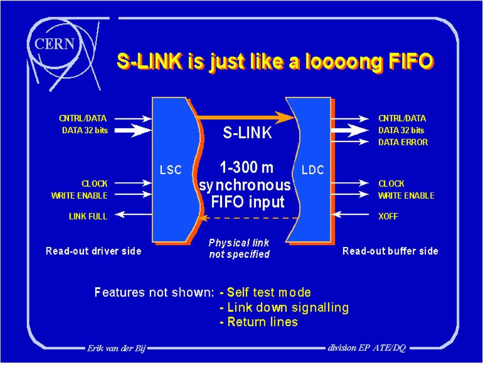
14 Pulsar design (cont.): From test stand tool to a general purpose tool Since there are some spare FPGA IO pins left, decided to use them to enhance Pulsar capability. A few simple modifications: (1) Add signal traces to P3 connector for SLINK IO, this allows Pulsar to interface directly with a PC via commercially available SLINK to PCI cards (2) Make L1 and SVT/XTRP inputs visible to all 3 FPGAs instead of just one FPGA Note: the mezzanine card connector is already compatible with SLINK mezzanine cards as both of them follow CMC standards. This allows us to test Pulsar prototype with SLINK test tools as well. Since the modification is simple enough at hardware level, it doesn t hurt to add them in, to make the board more general purpose. It provides the interface to a PC (via SLINK to PCI board) which could be very useful as a general purpose diagnostic tool. To learn more about SLINK, see CERN web page:

15

16
17 Level2_Pulsar design (as a tester only) 9U VME (VME FPGA not shown) 3 Altera APEX 20K400 FPGAs T S T R K Optical IO Mezz card connectors CDF ctrl Control L 1 T R K Optical IO With minor modifications: see next

18 Pulsar design (general purpose tool) 9U VME (VME FPGA not shown) 3 Altera APEX 20K400 FPGAs P1 T S S V T Data IO Mezz card connectors P2 user ctrl SLINK signal lines Control/ Merger P3 spare lines L 1 S V T Data IO With minor modifications

19 Front-panel (double width) LVDS connectors Mezzanine cards T S L 1 L 1 Mezzanine Card Hotlink/ Taxi/ S-LINK PULSAR design IO VME Ctrl optional user defined signal connection from P2/P3 S V T S V T IO SLINK S-LINK LDC or LSC S-LINK LDC or LSC component side Three FPGAs: Atlera APEX20K400 The mezzanine card connectors can be used either for user I/O or SLINK cards To/from Pulsar or a PC

20 Loaded with SLINK Mezzanine cards Can simply use CDF CAL backplane. CERN sent us two transition modules The transition module is very simple (just a few SLINK CMC connectors). It uses P2 type connector for P3. We will only use P3 for SLINK and spare (user defined) signals. (it doesn t have to be P2 type connector).
 signals.")
21 Examples of SLINK products LSC (Link Source Card), LDC (LINK Destination Card) Mezzanine card which can plug onto motherboard via CMC(Common Mezzanine Card) Connector (just like PMC). PCI to SLINK SLINK to PCI Proven technology, has been used by a few experiments to take hundreds of TB data in the past few years
22 New 32-bit SLINK to 64 bit PCI interface card: S32PCI64 highly autonomous data reception 32-bit SLINK, 64-bit PCI bus 33MHz and 66 MHz PCI clock speed up to 260MByte/s bandwidth High-speed follow up of the Simple SLINK to PCI interface card
23 SLINK format example: ATLAS SLINK data format
24 IO FPGA Control FPGA Pulsar Top Level schematics
25 MANY IO pins are assigned by hand to make the routing easier. Critical signals (clocks etc) are assigned by compiler with core working VHDL code. Pulsar components placement
26 Pulsar layout
27 Pulsar in pulser mode: hotlink examples: Optical IO Unit Muon case (only one mezzanine card shown) FIFO FIFO FIFO FIFO The latency is controlled by when the data is clocked out the FIFO Internal Test RAM controller SRAM L1A Buf #
28 load test pattern memory: use 36 bits data width, 32 will be for 4 fiber output (4 x 8), the highest 4 bits will be used as control bits to mark the content of data. For each event worth data, the first one will be the header, and the 32 bits data will contain the latency (&number of words etc) for this particular event and this particular path. The last one is the trailer, which can contain other info if needed (such as what L2 decision should be etc) (either use internal RAM or use 128K x 36 external SRAM, CY7C1350): 36bits Buffer0 data Buffer1 data Buffer2 data 4 Ctrl bits 8 bits data 8 bits data 8 bits data 8 bits data Buffer3 data The highest two address bits will be controlled by buffer number to divide automatically the memory for 4 buffers
29 How does it work: (1) after L1A, read the first word(header) and get the latency, at the same time start a counter; (2) continue to readout the rest of the data words from the memory and clock them into a FIFO, until the trailer is reached (can get the L2 decision information there) (3) once the counter reaches latency threshold, clock the data out from the FIFO at the speed which matches with the subsystem. this way the latency for each event and each data path can be individually controlled by user. Latency for this event, and other info header trailer data data data data 1 st event Other information (what L2 decision should be etc) One could have more control by inserting gaps in between data words etc using the 4 control bits, to better mimic the real situation for certain data paths. This approach seem to be quite flexible Buffer 0 data memory Ctrl bit 35: header Ctrl bit 34: trailer Ctrl bit 33: gap Ctrl bit 32: reserved
30 L1A Buf# RAM FIFO Initial thoughts on tester firmware design counter0 counter1 counter2 counter3 Buffer 0 data Latch L1A+buf# read 1 st word from RAM save latency&compare with counter continue reading data from RAM to FIFOs until last word once counter counts up to latency, enable FIFO output and ctrl signals for Tx chips ready for next L1A data ctrl FIFO FIFO FIFO FIFO ctrl VME Buffer 1 data Buffer 2 data 36bits addr Mezzanine Card side Buffer 3 data State machine
31 Comments: Pro: simple Con: not so elegant, as the state machine has to finish sending all data out of the FIFO before able to process next one. Maybe ok if run at higher clock rate. Will be some intrinsic delay between events. Possible implementation A: null L1A header Peter Wittich will talk about pulser mode firmware design detail and status soon. Good starting point, allow us to simulate the board soon. Would be better to separate the RAM to FIFO part from the actual data sending part output RAMtoFIFO Latency done
32 Possible implementation B: Comments: Pro: more elegant Con: somewhat more involved. null L1A counterq latency Output controller Implement this later for the real thing. header Data ready to be sent We decided to go for implementation A first. RAMtoFIFO FIFO done
33 hotlink examples: (only one mezzanine card shown) Pulsar in recorder mode (readout via VME) Optical IO Unit FIFO FIFO FIFO FIFO or controller L1A Buf # Configure the (S)RAM as a circular buffer for recording (for each L1A) and can be stopped and read out via VME. Internal Test RAM VME Each Optical IO FPGA looks at 8 fiber channels, SRAM has 32+4 bits. So need ping-ponging for recording (recording is at twice the incoming data rate, 60MHz) Natalia is working on this part of firmware SRAM
34 Pulsar in (general purpose) recorder mode (directly into a PC) Pulsar can convert any user data (via custom mezzanine cards) into SLINK format then transfer the data into a PC T S T R K Optical IO Mezzanine card connectors CDF ctrl Merger data PC SLINK to PCI SLINK L 1 T R K Optical IO ctrl Firmware: this mode exercises the whole board. The core firmware has been written in this mode and we have been simulating the whole board this way since April. Will talk about the details later. The firmware in this mode can be used initially to test the prototype board by using SLINK test tools.
35 L1A Buffer(2) Pulsar in recorder mode(into a PC): firmware design is similar to all three FPGAs L1A(x4) queue L1 trigger bits FIFO FIFO (pulls one event worth of data at a time) *Checks data consistence merges and stamp data SLINK Formatter 32-bit@40MHz FIFO SVT/XTRP data FIFO
36 Board Level simulation example
37 Pulsar firmware in CVS common: library for lower level VHDL code fpgapinmap: IO pin assignment files, compile setting files, VHDL templates etc Rx: VHDL code in various receiving modes Tx: VHDL code in various pulser modes crucial for team work and long term maintenance Pulsar is designed for long term maintenance for Level 2
38 Possible applications for Pulsar As Pulser for L2 decision crate: can source any data path as well as multiple paths at the same time As Recorder for L2: can record data from upstream for any data path (or multiple paths) As Pulser for Hit-Finder boards in SVT system: with a G-LINK mezzanine card, Pulsar can pulse SVT system by sending fiber data into Hit Finder boards: * can receive SVT cable input from Hit Finder output (for on-the-fly loop test) This could be important for long term maintenance for the system Can sink/source G-link/TAXI/HotLink/LVDS data for generic DAQ/trigger diagnostics. Other possible/potential applications: As a simple standalone DAQ system (in a test beam environment with custom mezz cards) can receive external trigger signals (NIM etc) via AUX card in the back maybe possible to use it as a general diagnostics tool for beams division? Future expansion is as cheap/fast/easy as designing a mezzanine card the rest are all commercially available The flexible design ( lego style ) makes it possible to use Pulsar as a general purpose tool within or outside CDF
39 Flexible design: Lego style philosophy The formation of Pulsar cluster
40 Board Level simulation and prototype testing plan Pulsar Mezzanine cards: hotlink Tx and Rx mezzanine cards have been simulated together, has a teststand setup at UC for prototype testing. Pulsar motherboard: Board Level simulation: intensive board level simulation in progress prepare for multi-board simulation: Pulsar + mezzanine cards schedule depends on board level simulation work the goal is to validate the design with INTENSIVE board level simulation by the end of June. Send out the prototype early July, and continue board level simulation a new visiting student (Sakari Pitkanen) from Finland just joined this effort Prototype testing plan: can use SLINK test tools first then test with custom mezzanine cards
41 Mezzanine cards board level simulation (1) 4 fiber case first (2) 2 fiber + LVDS case Natalia will talk about details later Transmitter Receiver This setup can test everything except CMC connectors
42 Mezzanine card Prototype/production test plan I (use the working teststand setup at UC): Pattern Generator (1) Use PG + LA; (2) Use FPGA internal RAM + LA (3) Use BIST + LA (hotlink) (run for long time and set limit on bit-error-rate to test for robustness) HP LA Transmitter Receiver This setup can test everything except CMC connectors
43 Pulsar + 4 hotlink mezzanine cards: prepare for multi-board simulation Mezzanine cards Pulsar
44 Initial test plan for Pulsar board prototype Pulsar board prototype can be first tested with SLINK test tools, then can be tested with custom mezzanine cards PULSAR IO M IO Slink out CPU Use SLINK source card to send data Use SLINK data sink to check data
45 SLIN data source test board SLINK data Drain test board (ideal for initial Pulsar prototype testing)
46 Prototype test plan II: use one Pulsar prototype board this would allow full tests (including the CMC connectors) Tx Rx I/O I/O M Mezzanine cards production can start ONLY AFTER the prototypes are tested with Pulsar prototype
The new frontier of the DATA acquisition using 1 and 10 Gb/s Ethernet links. Filippo Costa on behalf of the ALICE DAQ group
 The new frontier of the DATA acquisition using 1 and 10 Gb/s Ethernet links Filippo Costa on behalf of the ALICE DAQ group DATE software 2 DATE (ALICE Data Acquisition and Test Environment) ALICE is a
A+ Guide to Managing and Maintaining Your PC, 7e. Chapter 1 Introducing Hardware
 A+ Guide to Managing and Maintaining Your PC, 7e Chapter 1 Introducing Hardware Objectives Learn that a computer requires both hardware and software to work Learn about the many different hardware components
CCS Hardware Test and Commissioning Plan
 CCS Hardware Test and Commissioning Plan ECAL Off-Detector Electronics Workshop 7-8 April. 2005 Kostas Kloukinas CERN Overview CCS Development Status Production Plan CCS during Integration and Commissioning
Open Flow Controller and Switch Datasheet
 Open Flow Controller and Switch Datasheet California State University Chico Alan Braithwaite Spring 2013 Block Diagram Figure 1. High Level Block Diagram The project will consist of a network development
USB 3.0 Connectivity using the Cypress EZ-USB FX3 Controller
 USB 3.0 Connectivity using the Cypress EZ-USB FX3 Controller PLC2 FPGA Days June 20, 2012 Stuttgart Martin Heimlicher FPGA Solution Center Content Enclustra Company Profile USB 3.0 Overview What is new?
Instructions for Setting the T560 Digital Delay Generator for the Target Delay
 Instructions for Setting the T560 Digital Delay Generator for the Target Delay Important! These instructions are only to be followed by beam-line operators who have been trained to operate the target!!
Best Practises for LabVIEW FPGA Design Flow. uk.ni.com ireland.ni.com
 Best Practises for LabVIEW FPGA Design Flow 1 Agenda Overall Application Design Flow Host, Real-Time and FPGA LabVIEW FPGA Architecture Development FPGA Design Flow Common FPGA Architectures Testing and
PCIeBPMC (PCI/PCI-X Bus Compatible) Bridge based PCIe and PMC Compatible Adapter Carrier Front View shown with 1 installed fans model # PCIeBPMC-FAN2
 Bridge based PCIe and PMC Compatible Adapter Carrier Front View shown with 1 installed fans model # PCIeBPMC-FAN2") DE Store Home Company Search Design MadeInUSA White Papers PCIeBPMC PCIe [Express] to PMC Adapter / Carrier Shown with optional "Zero Slot Fans" in both positions. Fans available in either, both, or neither
DE Store Home Company Search Design MadeInUSA White Papers PCIeBPMC PCIe [Express] to PMC Adapter / Carrier Shown with optional "Zero Slot Fans" in both positions. Fans available in either, both, or neither
Designing VM2 Application Boards
 Designing VM2 Application Boards This document lists some things to consider when designing a custom application board for the VM2 embedded controller. It is intended to complement the VM2 Datasheet. A
Electron-Muon Ranger (EMR)
") Electron-Muon Ranger (EMR) Status of EMR Project R.Asfandiyarov 1, P.Béné 1, R.Bloch 1, A.Blondel 1, D.Bolognini 3 F.Cadoux 1, S.Débieux 1, J-S.Graulich 1, C.Husi 1, D.Lietti 3, F.Masciocchi 1, L.Nicola
Electron-Muon Ranger (EMR) Status of EMR Project R.Asfandiyarov 1, P.Béné 1, R.Bloch 1, A.Blondel 1, D.Bolognini 3 F.Cadoux 1, S.Débieux 1, J-S.Graulich 1, C.Husi 1, D.Lietti 3, F.Masciocchi 1, L.Nicola
Silicon Seminar. Optolinks and Off Detector Electronics in ATLAS Pixel Detector
 Silicon Seminar Optolinks and Off Detector Electronics in ATLAS Pixel Detector Overview Requirements The architecture of the optical links for the ATLAS pixel detector ROD BOC Optoboard Requirements of
RS-422/485 Multiport Serial PCI Card. RS-422/485 Multiport Serial PCI Card Installation Guide
 RS-422/485 Multiport Serial PCI Card Installation Guide 21 Contents 1. Introduction...1 2. Package Check List...2 3. Board Layouts and Connectors...3 3.1 2S with DB9 Male Connectors...3 3.1.1 JP5: UART
7a. System-on-chip design and prototyping platforms
 7a. System-on-chip design and prototyping platforms Labros Bisdounis, Ph.D. Department of Computer and Communication Engineering 1 What is System-on-Chip (SoC)? System-on-chip is an integrated circuit
AMC13 T1 Rev 2 Preliminary Design Review. E. Hazen Boston University. 2012-10-30 E. Hazen - AMC13 T1 V2 1
 13 T1 Rev 2 Preliminary Design Review E. Hazen Boston University 2012-10-30 E. Hazen - 13 T1 V2 1 Scope of this Review Background: 13 T1 board is being revised to support 10 GbE per request from CDAQ group
Silicon Lab Bonn. Physikalisches Institut Universität Bonn. DEPFET Test System Test Beam @ DESY
 Silicon Lab Bonn Physikalisches Institut Universität Bonn DEPFET Test System Test Beam @ DESY H. Krüger, EUDET Brainstorming, 3/4.11.2005 1 SI LAB DEPFET Prototype System DEPFET sensors 64 x 128 pixels,
Lab 1: Introduction to Xilinx ISE Tutorial
 Lab 1: Introduction to Xilinx ISE Tutorial This tutorial will introduce the reader to the Xilinx ISE software. Stepby-step instructions will be given to guide the reader through generating a project, creating
The 104 Duke_ACC Machine
 The 104 Duke_ACC Machine The goal of the next two lessons is to design and simulate a simple accumulator-based processor. The specifications for this processor and some of the QuartusII design components
Febex Data Acquisition System
 Febex Data Acquisition System (FPGA Hit Finder and Energy Filter for the FEBEX Pipelining ADC) Dr. Ivan Rusanov for CSEE, GSI - Darmstadt CSEE meeting, GSI 24.02.2014., Darmstadt The Febex Data AcquisitionSystem
Avoiding pitfalls in PROFINET RT and IRT Node Implementation
 Avoiding pitfalls in PROFINET RT and IRT Node Implementation Prof. Hans D. Doran ZHAW / Institute of Embedded Systems Technikumstrasse 9, 8400 Winterthur, Switzerland E-Mail: [email protected] Lukas Itin
Module 5. Broadcast Communication Networks. Version 2 CSE IIT, Kharagpur
 Module 5 Broadcast Communication Networks Lesson 1 Network Topology Specific Instructional Objectives At the end of this lesson, the students will be able to: Specify what is meant by network topology
DS1104 R&D Controller Board
 DS1104 R&D Controller Board Cost-effective system for controller development Highlights Single-board system with real-time hardware and comprehensive I/O Cost-effective PCI hardware for use in PCs Application
Development. Igor Sheviakov Manfred Zimmer Peter Göttlicher Qingqing Xia. AGIPD Meeting 01-02 April, 2014
 Textmasterformat AGIPD Firmware/Software bearbeiten Igor Sheviakov Manfred Zimmer Peter Göttlicher Qingqing Xia AGIPD Meeting 01-02 April, 2014 Outline Textmasterformat bearbeiten Reminder: hardware set-up
USB readout board for PEBS Performance test
 June 11, 2009 Version 1.0 USB readout board for PEBS Performance test Guido Haefeli 1 Li Liang 2 Abstract In the context of the PEBS [1] experiment a readout board was developed in order to facilitate
The modular concept of the MPA-3 system is designed to enable easy accommodation to a huge variety of experimental requirements.
 HARDWARE DESCRIPTION The modular concept of the MPA-3 system is designed to enable easy accommodation to a huge variety of experimental requirements. BASE MODULE GO LINE Digital I/O 8 Analog Out AUX 1
White Paper Utilizing Leveling Techniques in DDR3 SDRAM Memory Interfaces
 White Paper Introduction The DDR3 SDRAM memory architectures support higher bandwidths with bus rates of 600 Mbps to 1.6 Gbps (300 to 800 MHz), 1.5V operation for lower power, and higher densities of 2
Fondamenti su strumenti di sviluppo per microcontrollori PIC
 Fondamenti su strumenti di sviluppo per microcontrollori PIC MPSIM ICE 2000 ICD 2 REAL ICE PICSTART Ad uso interno del corso Elettronica e Telecomunicazioni 1 2 MPLAB SIM /1 MPLAB SIM is a discrete-event
AN10850. LPC1700 timer triggered memory to GPIO data transfer. Document information. LPC1700, GPIO, DMA, Timer0, Sleep Mode
 LPC1700 timer triggered memory to GPIO data transfer Rev. 01 16 July 2009 Application note Document information Info Keywords Abstract Content LPC1700, GPIO, DMA, Timer0, Sleep Mode This application note
1. Memory technology & Hierarchy
 1. Memory technology & Hierarchy RAM types Advances in Computer Architecture Andy D. Pimentel Memory wall Memory wall = divergence between CPU and RAM speed We can increase bandwidth by introducing concurrency
WHQL Certification Approval...2 User Interface...3 SUNIX s COMLab..4
 INDEX WHQL Certification Approval...2 User Interface....3 SUNIX s COMLab..4 1.0 Introduction...5 2.0 Specification..5 2.1 Features 2.2 Universal Serial PCI Card 2.3 RS-232 Specification 2.4 Low Profile
Welcome to the Introduction to Controller Area Network web seminar My name is William Stuart, and I am a Applications Engineer for the Automotive
 Welcome to the Introduction to Controller Area Network web seminar My name is William Stuart, and I am a Applications Engineer for the Automotive Products Group within Microchip. This web seminar today
Design and Verification of Nine port Network Router
 Design and Verification of Nine port Network Router G. Sri Lakshmi 1, A Ganga Mani 2 1 Assistant Professor, Department of Electronics and Communication Engineering, Pragathi Engineering College, Andhra
VME Data Acquisition System: Fundamentals and Beyond. Abhinav Kumar Bhabha Atomic Research Centre, Mumbai March 2011
 VME Data Acquisition System: Fundamentals and Beyond Abhinav Kumar Bhabha Atomic Research Centre, Mumbai March 2011 Presentation Outline Chapter 1 -------------------------------- Introduction to VME Chapter
ATLAS Tile Calorimeter Readout Electronics Upgrade Program for the High Luminosity LHC
 ATLAS Tile Calorimeter Readout Electronics Upgrade Program for the High Luminosity LHC Augusto Santiago Cerqueira On behalf of the ATLAS Tile Calorimeter Group Federal University of Juiz de Fora, Brazil
Computer Performance. Topic 3. Contents. Prerequisite knowledge Before studying this topic you should be able to:
 55 Topic 3 Computer Performance Contents 3.1 Introduction...................................... 56 3.2 Measuring performance............................... 56 3.2.1 Clock Speed.................................
AGIPD Interface Electronic Prototyping
 AGIPD Interface Electronic Prototyping P.Goettlicher I. Sheviakov M. Zimmer - Hardware Setup, Measurements - ADC (AD9252 14bit x 8ch x 50msps ) readout - Custom 10G Ethernet performance - Conclusions Test
MANUAL FOR RX700 LR and NR
 MANUAL FOR RX700 LR and NR 2013, November 11 Revision/ updates Date, updates, and person Revision 1.2 03-12-2013, By Patrick M Affected pages, ETC ALL Content Revision/ updates... 1 Preface... 2 Technical
MACHINE ARCHITECTURE & LANGUAGE
 in the name of God the compassionate, the merciful notes on MACHINE ARCHITECTURE & LANGUAGE compiled by Jumong Chap. 9 Microprocessor Fundamentals A system designer should consider a microprocessor-based
LLRF. Digital RF Stabilization System
 LLRF Digital RF Stabilization System Many instruments. Many people. Working together. Stability means knowing your machine has innovative solutions. For users, stability means a machine achieving its full
EZ DUPE DVD/CD Duplicator
 EZ DUPE DVD/CD Duplicator User s Manual Version 3.0 0 TABLE OF CONTENTS Introduction 2 Setup 11 LCD Front Panel Overview 2 o Auto Start Time 11 Menu Overview 3-5 o Display Mode 12 Functions 6 o Button
High speed pattern streaming system based on AXIe s PCIe connectivity and synchronization mechanism
 High speed pattern streaming system based on AXIe s connectivity and synchronization mechanism By Hank Lin, Product Manager of ADLINK Technology, Inc. E-Beam (Electron Beam) lithography is a next-generation
DS1621 Digital Thermometer and Thermostat
 Digital Thermometer and Thermostat www.dalsemi.com FEATURES Temperature measurements require no external components Measures temperatures from 55 C to +125 C in 0.5 C increments. Fahrenheit equivalent
TECHNOLOGY BRIEF. Compaq RAID on a Chip Technology EXECUTIVE SUMMARY CONTENTS
 TECHNOLOGY BRIEF August 1999 Compaq Computer Corporation Prepared by ISSD Technology Communications CONTENTS Executive Summary 1 Introduction 3 Subsystem Technology 3 Processor 3 SCSI Chip4 PCI Bridge
Enhancing High-Speed Telecommunications Networks with FEC
 White Paper Enhancing High-Speed Telecommunications Networks with FEC As the demand for high-bandwidth telecommunications channels increases, service providers and equipment manufacturers must deliver
MROD-X performance tests H. Boterenbrood, J. Vermeulen
 MRO-X performance tests H. Boterenbrood, J. Vermeulen ounter measures maximum trigger rate rigger vi out IM MRO RIN RG MRO MRO MRO Loopback fibers rigger vi: only used for random triggers Busy Busy and
Switch Fabric Implementation Using Shared Memory
 Order this document by /D Switch Fabric Implementation Using Shared Memory Prepared by: Lakshmi Mandyam and B. Kinney INTRODUCTION Whether it be for the World Wide Web or for an intra office network, today
Hello, and welcome to this presentation of the STM32 SDMMC controller module. It covers the main features of the controller which is used to connect
 Hello, and welcome to this presentation of the STM32 SDMMC controller module. It covers the main features of the controller which is used to connect the CPU to an SD card, MMC card, or an SDIO device.
ServoPAL (#28824): Servo Pulser and Timer
: Servo Pulser and Timer") Web Site: www.parallax.com Forums: forums.parallax.com Sales: [email protected] Technical: [email protected] Office: (916) 624-8333 Fax: (916) 624-8003 Sales: (888) 512-1024 Tech Support: (888) 997-8267
Web Site: www.parallax.com Forums: forums.parallax.com Sales: [email protected] Technical: [email protected] Office: (916) 624-8333 Fax: (916) 624-8003 Sales: (888) 512-1024 Tech Support: (888) 997-8267
USB - FPGA MODULE (PRELIMINARY)
") DLP-HS-FPGA LEAD-FREE USB - FPGA MODULE (PRELIMINARY) APPLICATIONS: - Rapid Prototyping - Educational Tool - Industrial / Process Control - Data Acquisition / Processing - Embedded Processor FEATURES:
DLP-HS-FPGA LEAD-FREE USB - FPGA MODULE (PRELIMINARY) APPLICATIONS: - Rapid Prototyping - Educational Tool - Industrial / Process Control - Data Acquisition / Processing - Embedded Processor FEATURES:
PCMCIA 1 Port RS232 2.1 EDITION OCTOBER 1999
 232 232232 PCMCIA 1 Port RS232 2.1 EDITION OCTOBER 1999 Guarantee. FULL 36 MONTHS GUARANTEE. We guarantee your interface card for a full 36 months from purchase, parts and labour, provided it has been
The data acquisition system of the XMASS experiment
 The data acquisition system of the XMASS experiment Katsuki Hiraide 1,2, for the XMASS Collaboration 1 Kamioka Observatory, Institute for Cosmic Ray Research, the University of Tokyo, Higashi-Mozumi, Kamioka,
How To Develop An Iterio Data Acquisition System For A Frustreo (Farc) (Iterio) (Fcfc) (For Aterio (Fpc) (Orterio).Org) (Ater
 (Iterio) (Fcfc) (For Aterio (Fpc) (Orterio).Org) (Ater") ITER Fast Plant System Controller Prototype Based on PXI Platform M.Ruiz & J.Vega on behalf of CIEMAT/UPM/IST/ITER team Universidad Politécnica de Madrid Asociación Euratom/CIEMAT IPFN, Instituto Superior
ITER Fast Plant System Controller Prototype Based on PXI Platform M.Ruiz & J.Vega on behalf of CIEMAT/UPM/IST/ITER team Universidad Politécnica de Madrid Asociación Euratom/CIEMAT IPFN, Instituto Superior
USBSPYDER08 Discovery Kit for Freescale MC9RS08KA, MC9S08QD and MC9S08QG Microcontrollers User s Manual
 USBSPYDER08 Discovery Kit for Freescale MC9RS08KA, MC9S08QD and MC9S08QG Microcontrollers User s Manual Copyright 2007 SofTec Microsystems DC01197 We want your feedback! SofTec Microsystems is always on
Application Note 132. Introduction. Voice Video and Data Communications using a 2-Port Switch and Generic Bus Interface KSZ8842-16MQL/MVL
 Application Note 132 Voice Video and Data Communications using a 2-Port Switch and Generic Bus Interface KSZ42-16MQL/MVL Introduction The IP-Telephony market is booming, due to the ease of use of the technology
What is LOG Storm and what is it useful for?
 What is LOG Storm and what is it useful for? LOG Storm is a high-speed digital data logger used for recording and analyzing the activity from embedded electronic systems digital bus and data lines. It
APPLICATION NOTE GaGe CompuScope 14200-based Lightning Monitoring System
 APPLICATION NOTE GaGe CompuScope 14200-based Lightning Monitoring System Challenge A customer needed to upgrade an older data acquisition unit for a real-time lightning monitoring system. Unlike many lightning
The CP 342-5 FO provides access to different communication services of the PROFIBUS bus system:
 CP 342-5 FO Function The CP 342-5 FO provides access to different communication services of the PROFIBUS bus system: PROFIBUS DP (according to IEC 61 158/61784, master or slave) PG/OP communication S7
GETTING STARTED WITH STUDIO ONE ARTIST
 GETTING STARTED WITH STUDIO ONE ARTIST 2009, PreSonus Audio Electronics, Inc. All Rights Reserved. TABLE OF CONTENTS Studio One Artist Features...3 System Requirements...4 Installation and Authorization...5
Introduction to Programmable Logic Devices. John Coughlan RAL Technology Department Detector & Electronics Division
 Introduction to Programmable Logic Devices John Coughlan RAL Technology Department Detector & Electronics Division PPD Lectures Programmable Logic is Key Underlying Technology. First-Level and High-Level
Lesson 10: Video-Out Interface
 Lesson 10: Video-Out Interface 1. Introduction The Altera University Program provides a number of hardware controllers, called cores, to control the Video Graphics Array (VGA) Digital-to-Analog Converter
DS1621 Digital Thermometer and Thermostat
 www.maxim-ic.com FEATURES Temperature measurements require no external components Measures temperatures from -55 C to +125 C in 0.5 C increments. Fahrenheit equivalent is -67 F to 257 F in 0.9 F increments
We will be covering the following topics in this document:
 ÂØÒňΠSupplemental Notes External Sequencing with the MC-505 November 15th, 1998 SN95 v1.0 As you know, the MC-505 Groove Box is a great instrument for creating grooves as well as for realtime control
CMS Tracker module / hybrid tests and DAQ development for the HL-LHC
 CMS Tracker module / hybrid tests and DAQ development for the HL-LHC S. Mersi, G. Auzinger [email protected] 1 Outline Reminder: the Ph2 CMS Tracker upgrade pt Modules: principle, elements, electronics
Using Altera MAX Series as Microcontroller I/O Expanders
 2014.09.22 Using Altera MAX Series as Microcontroller I/O Expanders AN-265 Subscribe Many microcontroller and microprocessor chips limit the available I/O ports and pins to conserve pin counts and reduce
Chapter 4 System Unit Components. Discovering Computers 2012. Your Interactive Guide to the Digital World
 Chapter 4 System Unit Components Discovering Computers 2012 Your Interactive Guide to the Digital World Objectives Overview Differentiate among various styles of system units on desktop computers, notebook
The Bus (PCI and PCI-Express)
") 4 Jan, 2008 The Bus (PCI and PCI-Express) The CPU, memory, disks, and all the other devices in a computer have to be able to communicate and exchange data. The technology that connects them is called the
4 Jan, 2008 The Bus (PCI and PCI-Express) The CPU, memory, disks, and all the other devices in a computer have to be able to communicate and exchange data. The technology that connects them is called the
Download the Design Files
 Design Example Using the altlvds Megafunction & the External PLL Option in Stratix II Devices March 2006, ver. 1.0 Application Note 409 Introduction The altlvds megafunction allows you to instantiate an
OUTLINE SPECIFICATIONS FOR THE VME MOUNT MODULE AND TCM IN SLOTS 1 & 21.
 OUTLINE SPECIFICATIONS FOR THE VME MOUNT MODULE AND TCM IN SLOTS 1 & 21. WHY TCM ETC TRIGGER PRESSOR MODULES REQUIRE AN INPUT OF LHC CLKS AND CONTROLS via THE TTC SYSTEM --- AND ACCESS TO THE DCS SYSTEM
How to build a high speed PCI Express bus expansion system using the Max Express product family 1
 Applications The Anatomy of Max Express Cable Expansion How to build a high speed PCI Express bus expansion system using the Max Express product family 1 By: Jim Ison Product Marketing Manager One Stop
Displayport Extender via 2 multimode fibers LC Duplex Connector Extends Displayport Link up to 200 meters
 Description Displayport combines the audio and video through an interface. It supports high resolution displays and multiple displays with a single cable, and increases the efficiency and bandwidth of
Surveillance System Using Wireless Sensor Networks
 Surveillance System Using Wireless Sensor Networks Dan Nguyen, Leo Chang Computer Engineering, Santa Clara University Santa Clara, California, USA [email protected] [email protected] Abstract The
TURBO PROGRAMMER USB, MMC, SIM DEVELOPMENT KIT
 TURBO PROGRAMMER USB, MMC, SIM DEVELOPMENT KIT HARDWARE GUIDE This document is part of Turbo Programmer documentation. For Developer Documentation, Applications and Examples, see http:/// PRELIMINARY (C)
In-System Programming Design TM. Guidelines for ispjtag Devices. Introduction. Device-specific Connections. isplsi 1000EA Family.
 In-System Design TM February 2002 Introduction In-system programming (ISP ) has often been billed as a direct replacement for configuring a device through a programmer. The idea that devices can simply
Web Site: www.parallax.com Forums: forums.parallax.com Sales: [email protected] Technical: [email protected]
 Web Site: www.parallax.com Forums: forums.parallax.com Sales: [email protected] Technical: [email protected] Office: (916) 624-8333 Fax: (916) 624-8003 Sales: (888) 512-1024 Tech Support: (888) 997-8267
Development of the electromagnetic calorimeter waveform digitizers for the Fermilab Muon g-2 experiment
 Development of the electromagnetic calorimeter waveform digitizers for the Fermilab g-2 experiment 1 on behalf of the Fermilab E989 g-2 Collaboration European Physical Society Conference on High Energy
Design of a High Speed Communications Link Using Field Programmable Gate Arrays
 Customer-Authored Application Note AC103 Design of a High Speed Communications Link Using Field Programmable Gate Arrays Amy Lovelace, Technical Staff Engineer Alcatel Network Systems Introduction A communication
RCC2 Test Proceedures
 RCC2 Test Proceedures 1. Power-up Test 1. install board in VME crate (6U style or 6U section of 9U) and turn on power 2. check that cfg LED (D4) on front panel and D3 LED on board near U47 are lit (red)
FPGA Synthesis Example: Counter
 FPGA Synthesis Example: Counter Peter Marwedel Informatik XII, U. Dortmund Gliederung Einführung SystemC Vorlesungen und Programmierung FPGAs - Vorlesungen - VHDL-basierte Konfiguration von FPGAs mit dem
LAB #3 VHDL RECOGNITION AND GAL IC PROGRAMMING USING ALL-11 UNIVERSAL PROGRAMMER
 LAB #3 VHDL RECOGNITION AND GAL IC PROGRAMMING USING ALL-11 UNIVERSAL PROGRAMMER OBJECTIVES 1. Learn the basic elements of VHDL that are implemented in Warp. 2. Build a simple application using VHDL and
EE482: Advanced Computer Organization Lecture #11 Processor Architecture Stanford University Wednesday, 31 May 2000. ILP Execution
 EE482: Advanced Computer Organization Lecture #11 Processor Architecture Stanford University Wednesday, 31 May 2000 Lecture #11: Wednesday, 3 May 2000 Lecturer: Ben Serebrin Scribe: Dean Liu ILP Execution
Results of Benchmark Tests upon a Gigabit Ethernet Switch
 Results of Benchmark Tests upon a Gigabit Ethernet Switch LHCb Technical Note Issue: Draft Revision: 1 Reference: LHCb DAQ 2001-nn Created: 13 th August 2001 Last modified: 17 th August 2001 Prepared By:
In-System Programmer USER MANUAL RN-ISP-UM RN-WIFLYCR-UM-.01. www.rovingnetworks.com 1
 RN-WIFLYCR-UM-.01 RN-ISP-UM In-System Programmer 2012 Roving Networks. All rights reserved. Version 1.1 1/19/2012 USER MANUAL www.rovingnetworks.com 1 OVERVIEW You use Roving Networks In-System-Programmer
Timer A (0 and 1) and PWM EE3376
 and PWM EE3376") Timer A (0 and 1) and PWM EE3376 General Peripheral Programming Model Each peripheral has a range of addresses in the memory map peripheral has base address (i.e. 0x00A0) each register used in the peripheral
Timer A (0 and 1) and PWM EE3376 General Peripheral Programming Model Each peripheral has a range of addresses in the memory map peripheral has base address (i.e. 0x00A0) each register used in the peripheral
Discovering Computers 2011. Living in a Digital World
 Discovering Computers 2011 Living in a Digital World Objectives Overview Differentiate among various styles of system units on desktop computers, notebook computers, and mobile devices Identify chips,
What is a bus? A Bus is: Advantages of Buses. Disadvantage of Buses. Master versus Slave. The General Organization of a Bus
 Datorteknik F1 bild 1 What is a bus? Slow vehicle that many people ride together well, true... A bunch of wires... A is: a shared communication link a single set of wires used to connect multiple subsystems
UMBC. ISA is the oldest of all these and today s computers still have a ISA bus interface. in form of an ISA slot (connection) on the main board.
 on the main board.") Bus Interfaces Different types of buses: ISA (Industry Standard Architecture) EISA (Extended ISA) VESA (Video Electronics Standards Association, VL Bus) PCI (Periheral Component Interconnect) USB (Universal
Bus Interfaces Different types of buses: ISA (Industry Standard Architecture) EISA (Extended ISA) VESA (Video Electronics Standards Association, VL Bus) PCI (Periheral Component Interconnect) USB (Universal
PCI Express IO Virtualization Overview
 Ron Emerick, Oracle Corporation Author: Ron Emerick, Oracle Corporation SNIA Legal Notice The material contained in this tutorial is copyrighted by the SNIA unless otherwise noted. Member companies and
MODULE BOUSSOLE ÉLECTRONIQUE CMPS03 Référence : 0660-3
 MODULE BOUSSOLE ÉLECTRONIQUE CMPS03 Référence : 0660-3 CMPS03 Magnetic Compass. Voltage : 5v only required Current : 20mA Typ. Resolution : 0.1 Degree Accuracy : 3-4 degrees approx. after calibration Output
9/14/2011 14.9.2011 8:38
 Algorithms and Implementation Platforms for Wireless Communications TLT-9706/ TKT-9636 (Seminar Course) BASICS OF FIELD PROGRAMMABLE GATE ARRAYS Waqar Hussain [email protected] Department of Computer
DESIGN AND VERIFICATION OF LSR OF THE MPLS NETWORK USING VHDL
 IJVD: 3(1), 2012, pp. 15-20 DESIGN AND VERIFICATION OF LSR OF THE MPLS NETWORK USING VHDL Suvarna A. Jadhav 1 and U.L. Bombale 2 1,2 Department of Technology Shivaji university, Kolhapur, 1 E-mail: [email protected]
Semiconductor Device Technology for Implementing System Solutions: Memory Modules
 Hitachi Review Vol. 47 (1998), No. 4 141 Semiconductor Device Technology for Implementing System Solutions: Memory Modules Toshio Sugano Atsushi Hiraishi Shin ichi Ikenaga ABSTRACT: New technology is producing
GETTING STARTED WITH PROGRAMMABLE LOGIC DEVICES, THE 16V8 AND 20V8
 GETTING STARTED WITH PROGRAMMABLE LOGIC DEVICES, THE 16V8 AND 20V8 Robert G. Brown All Rights Reserved August 25, 2000 Alta Engineering 58 Cedar Lane New Hartford, CT 06057-2905 (860) 489-8003 www.alta-engineering.com
Lab 1 Course Guideline and Review
 Lab 1 Course Guideline and Review Overview Welcome to ECE 3567 Introduction to Microcontroller Lab. In this lab we are going to experimentally explore various useful peripherals of a modern microcontroller
A Scalable Large Format Display Based on Zero Client Processor
 International Journal of Electrical and Computer Engineering (IJECE) Vol. 5, No. 4, August 2015, pp. 714~719 ISSN: 2088-8708 714 A Scalable Large Format Display Based on Zero Client Processor Sang Don
21152 PCI-to-PCI Bridge
 Product Features Brief Datasheet Intel s second-generation 21152 PCI-to-PCI Bridge is fully compliant with PCI Local Bus Specification, Revision 2.1. The 21152 is pin-to-pin compatible with Intel s 21052,
Technical Information Manual
 Technical Information Manual Revision n.1 4 January 2004 Mod. Table of Contents TABLE OF CONTENTS... I 1 GENERAL DESCRIPTION...1 1.1 OVERVIEW...1 1.2 MAIN TECHNICAL SPECIFICATIONS...1 2 FUNCTIONAL DESCRIPTION...2
CSE2102 Digital Design II - Topics CSE2102 - Digital Design II
 CSE2102 Digital Design II - Topics CSE2102 - Digital Design II 6 - Microprocessor Interfacing - Memory and Peripheral Dr. Tim Ferguson, Monash University. AUSTRALIA. Tel: +61-3-99053227 FAX: +61-3-99053574
Transmission of High-Speed Serial Signals Over Common Cable Media
 Transmission of High-Speed Serial February 0 Introduction Technical Note TN066 Designers are often faced with moving serial data from one location to another, over moderate distances, and in the most efficient
Live Recording with M7CL-48ES & AuviTran Network ASIO Streamer. Using Steinberg Cubase 5 or Nuendo 5.
 & AuviTran Network ASIO Streamer Using Steinberg Cubase 5 or Nuendo 5. Summary: This guide shows how quick and easy it is to achieve a high quality, live multitrack recording using Yamaha M7CL-48ES, stage-boxes
Technical Note. Micron NAND Flash Controller via Xilinx Spartan -3 FPGA. Overview. TN-29-06: NAND Flash Controller on Spartan-3 Overview
 Technical Note TN-29-06: NAND Flash Controller on Spartan-3 Overview Micron NAND Flash Controller via Xilinx Spartan -3 FPGA Overview As mobile product capabilities continue to expand, so does the demand