TRANSISTOR AMPLIFIERS AET 8. First Transistor developed at Bell Labs on December 16, 1947
|
|
|
- Aleesha Underwood
- 9 years ago
- Views:
Transcription
1 AET 8 First Transistor developed at Bell Labs on December 16, 1947

2 Objective 1a Identify Bipolar Transistor Amplifier Operating Principles

3 Overview (1) Dynamic Operation (2) Configurations (3) Common Emitter (4) Common Collector (5) Common Base (6) Temperature Stabilization (7) Coupling
 Temperature Stabilization (7)")
4 Typical Amplifier
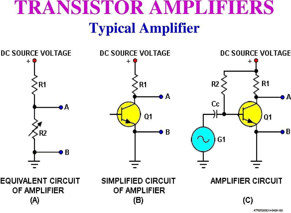
5 Typical Amplifier (A). Output taken from A to B: Reduce the resistance of R2, voltage from A to B decreases. Increase the resistance of R2, voltage from A to B increases. (Voltage follows resistance)!

6 Typical Amplifier Resistor (R2) is replaced with transistor (Q1) (B). Output taken from A to B: Reduce the resistance of Q1, voltage from A to B decreases. Increase the resistance of Q1, voltage from A to B increases. (Voltage follows resistance)!

7 Typical Amplifier (C)An input signal from G1 is applied to the base through C C. The input signal changes the Bias on the base of the transistor controlling the current flow through the transistor. The output, taken from A to B, will be a reproduction of the input signal only much larger.

8 Amplification: The ability of a circuit to receive a small change of input voltage or current (signal) and produce a large change in the output voltage or current (signal). Amplification depends on the change in the transistor s resistance caused by an input signal.

9 CONFIGURATIONS

10 Common Emitter Common Emitter is sometimes called the Grounded Emitter. Input signal is applied to the base. Output signal is taken from the collector. The common line, (not used for signal) is connected to the emitter.
 is connected to")
11 Common Collector Common Collector (CC) is sometimes called Grounded Collector. The input signal is applied to the base. The output signal is taken from the emitter. The common line, (not used for signal) is connected to the collector.

12 Common Base Common Base (CB) is sometimes called Grounded Base. The input signal is applied to the emitter. The output signal is taken from the collector. The common line, (not used for signal) is connected to the base.

13 Common Emitter Amplifier The purpose of the common emitter amplifier is to provide good current, voltage, and power gain. 180 phase shift

14 Common Emitter Amplifier Components R 1 determines forward bias R 2 aids in developing bias R 3 is the collector load resistor used to develop the output signal R 4 is the emitter resistor used for thermal stability

15 Common Emitter Amplifier Components Q 1 - transistor C 1 is the input coupling capacitor

16 Common Emitter Amplifier Current paths and percentage of flow I E = 100%, I C = 95%, I B = 5% NPN Current flows from Ground to +VCC

17 Common Emitter Amplifier Signal path: When a signal is applied to an amplifier, four things occur. Base, emitter & collector currents change at the rate of the input signal Collector voltage changes at the rate of the input signal Phase shift of 180 There will be signal gain!

18 Common Emitter Amplifier Static or Quiescent Operation By definition, bias is defined as the average DC voltage (or current) used to establish the operating point in transistor circuits for a static or quiescent condition. A static condition means the circuit does not have an input signal and is fixed in a non-varying condition.

19 Typical Amplifier with Bias - Static Condition Transistor Current Path 600mv (.6v) Bias (emitter to base voltage) causes emitter current (IE), base current (IB), and collector current (IC) to flow.
, base current (IB), and collector")
20 Typical Amplifier with Bias - Static Condition Current enters the emitter and exits the base. Current enters the emitter and exits the collector through R1 to V CC.

21 Common Emitter Amplifier Dynamic Operation The varying condition of a circuit is called its dynamic condition or operating condition. This occurs whenever an input signal is applied.
22 Typical Amplifier with Bias - Dynamic Dynamic condition: DC Bias with signal added (Varying condition) The output voltage has a much larger voltage change than the input.
23 Typical Amplifier with Bias - Dynamic Notice the.2v Pk-Pk signal at the input is using the.6v DC as its reference and the output 10V Pk-Pk signal is using the 15V DC as its reference.
24 Common Emitter Amplifier
25 NPN Common Emitter Amplifier Operation The negative alternation of the input signal applied to the base of the transistor causes forward bias to decrease and collector current to decrease. The voltage drop across R 3 decreases because I C decreased The collector voltage (V C ) increases The bias decrease caused an increase in output voltage and produced a 180 phase inversion
26 NPN Common Emitter Amplifier Operation The positive alternation of the input signal applied to the base causes forward bias to increase and collector current to increase The voltage drop across R 3 increases because I C increased The collector voltage (V C ) decreases The bias increase caused a decrease in output voltage and produced a 180 phase inversion
27 Common Emitter Amplifier
28 Common Emitter Amplifier NPN with conventional power connection V CC to base and collector using respective resistors (R 1 & R 2 ).
29 Common Emitter Amplifier NPN with alternate power connection V EE to emitter with current path through Q 1 out the base and collector through R 1 & R 2 to ground.
30 Common Emitter Amplifier PNP with conventional power connection -V CC to base and collector using respective resistors (R 1 & R 2 ).
31 Common Emitter Amplifier PNP with alternate power connection +V EE to emitter with current path in the base and collector through R 1 & R 2 out the emitter to ground.
32 Common Emitter Amplifier Characteristic Curve Graph A transistor CHARACTERISTIC CURVE is a graph plotting of the relationships between currents and voltages in a transistor circuit. The graph is then called a FAMILY of curves.
33 Common Emitter Amplifier Characteristic Curve Graph Graph shows base current (I B ) changes vs. collector current (I C ). Graph shows a change in V CC vs. I C
34 Point A -Cutoff Point B -Saturation Base current - I B
35 Common Emitter Amplifier Amplifier Gain A ratio of the change in output to the change in input expressed as a formula:
36 Common Emitter Amplifier Bias vs. Gain Characteristics Optimum has the best gain R 2 is directly proportional to bias, resistance increases forward bias increases R 1 is inversely proportional to bias
37 Common Emitter Amplifier Collector Load Resistor Changes Increasing the resistance of R3 will cause a corresponding increase in the amount of change in collector voltage and increase in voltage gain. Gain is directly proportional to the resistance value of R3.
38 Increasing R2 to 6KΩ changes the load line and gain increases from 10V to 12.5 volts. Point B-Saturation
39 Class of Operation There are four classes of operation for amplifiers: A, AB, B and C The class of operation is determined by the amount of forward bias.
40 Common Emitter Amplifier Class A Class A amplifiers have an exact reproduction of the input in the output. Conducts 100% of the time The collector current will flow for 360 degrees of the input signal
41 Class A Amplifier Curve Saturation Q-Point I C 90 ua 80 ua 70 ua 60 ua 50 ua 40 ua 30 ua 20 ua 10 ua 0 ua I B Cutoff V CE
42 Common Emitter Amplifier Class AB Class AB amplifiers has some amplitude distortion and conducts 51% to 99% of the time.
43 Class AB Amplifier Curve I C 90 ua 80 ua 70 ua I B Saturation 60 ua 50 ua 40 ua 30 ua Q-Point 20 ua 10 ua 0 ua Cutoff V CE
44 Common Emitter Amplifier Class B Class B amplifiers has amplitude and crossover distortion. Conducts 50% of the time. The collector current will flow for 180 degrees of the input signal.
45 Class B Amplifier Curve I C 90 ua 80 ua 70 ua I B Saturation 60 ua 50 ua 40 ua 30 ua Q-Point 20 ua 10 ua 0 ua Cutoff V CE
46 Common Emitter Amplifier Class C Class C amplifiers have amplitude and crossover distortion on both alternations. Conducts < 50%
47 Class C Amplifier Curve I C 90 ua 80 ua 70 ua I B Saturation 60 ua 50 ua 40 ua 30 ua 20 ua 10 ua Cutoff V CE 0 ua Q-Point
48 Fidelity The degree to which a device accurately reproduces at its output the characteristics of its input signal. Class A has the best fidelity Efficiency The ratio between the output signal power and the total input power. Class C has the best efficiency.
49 Amplitude Distortion The result of changing a waveshape so its amplitude is no longer proportional to the original amplitude. Amplitude distortion caused by too large input signal, excessive bias, or insufficient forward bias.
50 Class of Operation Chart
51 Common Base Amplifier The common base amplifier is also known as the grounded base amplifier. The common base amplifier has a voltage gain greater than one, but it has a current gain less than one. It is normally characterized by a very small input impedance and a high output impedance like the common emitter amplifier. The input signal is in phase with the output signal.
52 Common Base Amplifier R 1 provides forward bias for the emitterbase junction R 2 aids in developing forward bias R 3 is the collector load resistor R 4 develops the input signal
53 Common Base Amplifier C 1 places the base at AC ground C 2 is the input coupling capacitor C 3 is the Output coupling capacitor Q 1 NPN transistor
54 Common Base Amplifier A positive alternation applied to the emitter of the transistor decreases forward bias and causes emitter current to decrease. A decrease in emitter current results in a decrease in collector current. A decrease in I C decreases E R3, causing V C to become more positive. The collector waveform is an amplified reproduction of the positive input alternation.
55 Common Collector Amplifier The common collector amplifier is also called the emitter follower amplifier because the output voltage signal at the emitter is approximately equal to the input signal on the base. Amplifier's voltage gain is always less than the input signal voltage. Used to match a high-impedance source to a low-impedance load
56 Common Collector Amplifier Common collector amplifier has a large current and power gain, excellent stability and frequency response. The output impedance of this circuit is equal to the value of the emitter resistor, this circuit is used for impedance matching. The input and output signals are in phase.
57 Common Collector Amplifier Uses degenerative or negative feedback. Degenerative feedback is the process of returning a part of the output of an amplifier to its input in such a manner that it cancels part of the input signal. As a result, the common collector amplifier has a voltage gain of less than 1.
58 Common Collector Amplifier
59 Common Collector Amplifier R1 Determines amplifier forward bias R2 Aids in determining forward bias R3 Emitter load resistor-develops the output signal & degenerative feedback C1 Input coupling capacitor C2 By-pass capacitor, places collector at AC ground C3 Output coupling capacitor Q1 Transistor amplifier
60 Common Collector Amplifier As the voltage on the base goes in a positive direction, the voltage on the emitter goes in a positive direction. This positive voltage reverse biases the transistor decreasing I C resulting in an increase voltage drop across the transistor.
61 Common Collector Amplifier As the voltage drop across the transistor increases the voltage drop across the load resistor R 3 decreases, thus gain less than one.
62 Appraisal
63 1. In the common emitter configuration, the input is applied to the and the output is taken from the. a. emitter; collector b. base; collector c. emitter; base d. base; emitter
64 2. What is the purpose of resistors R1 and R2? a. Amplify the input signal b. Develop the output signal c. Develop forward bias voltage for Q1 d. Block DC from the base of Q1
65 3. In a common collector amplifier, degenerative feedback is out of phase with the input signal. a. 0 degrees b. 90 degrees c. 180 degrees d. 270 degrees
66 4. The common base amplifier has a voltage gain, but a current gain. a. less than one, less than one b. greater than one, less than one c. less than one, greater than one d. greater than one, greater than one
67 5. In the common emitter configuration, R3 primarily affects a. gain. b. forward bias. c. degeneration. d. temperature stabilization.
68 6. What is the purpose of R4 in the common base amplifier? a. Couple the output signal b. Develop the input signal c. Develop the output signal d. Keep the base at AC ground
69 7. In the amplifier circuit shown, the purpose of C2 is to a. couple the output signal. b. develop the output signal. c. place the collector at AC ground. d. provide regenerative feeback.
70 8. The amplifiers class of operation is determined by a. fidelity. b. efficiency. c. output waveform. d. amount of forward bias.
71 9. With a transistor amplifier operating in class B, the collector current will flow for of the input signal. a. 90 degrees b. 180 degrees c. 360 degrees d. more than 180 degrees but less than 360 degrees
72 10. In the transistor amplifier shown, what is the phase relationship between the input and output signals? a. 0 degree phase shift b. 90 degree phase shift c. 180 degree phase shift d. 270 degree phase shift
73 TRANSISTOR AMPLIFIER TEMPERATURE STABALIZATION
74 TEMPERATURE STABALIZATION PURPOSE The process of minimizing undesired changes in a transistor circuit caused by heat is called temperature stabilization.
75 TEMPERATURE STABALIZATION Negative Temperature Coefficient Transistors have a negative temperature coefficient This means that as temperature increases the resistance of the transistor decreases.
76 TEMPERATURE STABALIZATION Negative Temperature Coefficient To compensate for temperature changes, all thermal stabilization circuits do the opposite to the transistor. As temperature increases, the thermal stabilization circuits reduce forward bias of the transistor, increasing its resistance.
77 TEMPERATURE STABALIZATION Collector Current (I C ) vs.temperature Graph Non-stabilized circuits As temperature increases I C increases due to the resistance of the transistor decreasing. This causes the transistor I C to move above its operating point.
78 TEMPERATURE STABALIZATION Swamping Resistor Stabilization
79 TEMPERATURE STABALIZATION Swamping Resistor Stabilization Placing a resistor (R 3 ) in the emitter for temperature stabilization is referred to as a Swamping resistor. Using swamping resistor (R 3 ) for temperature stabilization results in degeneration feedback. An increase in I C flows through the emitter resistor and develops an increase in voltage on the emitter. This voltage opposes forward bias and reduces I B and I C.
80 TEMPERATURE STABALIZATION Swamping Resistor with Bypass Capacitor
81 TEMPERATURE STABALIZATION Swamping Resistor with Bypass Capacitor C 2 is referred to as the emitter bypass capacitor. By placing a large capacitor (C 2 ) across R 3, a signal ground is established and compensates for signal degeneration
82 TEMPERATURE STABALIZATION Thermistor Stabilization
83 TEMPERATURE STABALIZATION Thermistor Stabilization A thermistor has a negative temperature coefficient of resistance. Bias is established by R 1 and R T1 the thermistor. As temp. increases, resistance of R T1 decreases, causing bias and I C to decrease This compensates for the change in I C due to temp. variations.
84 TEMPERATURE STABALIZATION Forward Bias Diode Stabilization.
85 TEMPERATURE STABALIZATION Forward Bias Diode Stabilization To more closely follow resistance changes of the transistor, replace the thermistor with a diode. Diodes and transistors are made of the same materials, therefore, closely follow temperature changes. As the amplifiers forward biased diode temperature increases its resistance decreases, thus forward bias decreases.
86 TEMPERATURE STABALIZATION Reverse Bias Diode Stabilization
87 TEMPERATURE STABALIZATION Reverse Bias Diode Stabilization Used to reduce the effects of I CB on collector current. As the reverse current of CR 1 increases, it will cause a larger voltage drop across R 1. This will reduce the voltage across the baseemitter junction (V EB ), causing base current to decrease, causing collector current will decrease.
88 TEMPERATURE STABALIZATION Double Diode Stabilization
89 TEMPERATURE STABALIZATION Double Diode Stabilization Forward biased diode CR 1 compensates for changes in the resistance of the forward biased emitter-base junction due to temperature. The reverse biased diode CR 2 compensates for the effects of I CB in the reverse biased collector-base junction.
90 TEMPERATURE STABALIZATION Heat Sink Heat sinks dissipate heat generated by high current through transistors The transistor is connected directly to the heat sink and the fins dissipate the heat away from the junctions.
91 TEMPERATURE STABILIZATION Appraisal
92 TEMPERATURE STABILIZATION 11. The negative temperature coefficient of a thermistor means that as temperature increases resistance. a. increases b. decreases c. Remains the same
93 TEMPERATURE STABILIZATION 12. Using the swamping resistor for thermal stability, what type of feedback is developed to control the amplifier? a. Regenerative b. Degenerative c. Positive feedback
94 TEMPERATURE STABILIZATION 13. Which of the following devices is used to dissipate heat into the air? a. Heat sink b. Circuit board c. Swamping resistor d. Coupling capacitor
95 TRANSISTOR AMPLIFIER COUPLING
96 TRANSISTOR AMPLIFIER COUPLING Purpose: To achieve the high gain needed by most circuits, amplifiers are connected in series (or cascaded together) to form cascade amplifiers. The signal is couple from one amplifier stage to another.
97 TRANSISTOR AMPLIFIER COUPLING Cascade Amplifier Voltage Gain Low gain amplifiers do not amplify the input signal enough to be of practical use. Using cascade amplifiers, high gain is achieved without incurring distortion. The overall gain of a cascade amplifier is equal to the product of the individual gains, or: A V(TOTAL) = A V1 x A V2 x A V3
98 TRANSISTOR AMPLIFIER COUPLING Cascade Amplifier Voltage Gain The overall gain for this cascade amplifier, however, is 1000 (A V(TOTAL) = A V1 x A V2 x A V3 = 10 x 10 x 10 = 1000).
99 TRANSISTOR AMPLIFIER COUPLING There are numerous types of circuits used to connect (or couple) one amplifier to another. The most commonly used are: Direct Coupling RC Coupling LC Coupling Transformer Coupling
100 Direct, RC, LC, and Transformer Coupling
101 LOW FREQUENCY GAIN LOSS Three types of components cause low frequency gain loss in a cascade amplifier: coupling capacitors, inductors and transformers. Coupling Capacitors cause low frequency gain loss because of their high capacitive reactance at low frequencies. Inductors and Transformers cause low frequency gain loss at low frequencies for the opposite reason. They have low reactance at low frequencies.
102 HIGH FREQUENCY GAIN LOSS Components that cause high frequency gain loss are transistors, inductors and transformers. Stray capacitance caused by various wires and components will also cause high frequency gain loss.
103 HIGH FREQUENCY GAIN LOSS Transistors - Interelement Capacitance The emitter-base and collector-base junctions form an effective capacitance at high frequencies. The signal bypasses the transistor thus preventing amplification. Interelement capacitance causes loss of signal at high frequencies.
104 HIGH FREQUENCY GAIN LOSS Inter-winding Capacitance High frequency loss is due to interwinding capacitance in which the individual coils can act as capacitors. Only occurs at very high frequencies.
105 HIGH FREQUENCY GAIN LOSS Stray Capacitance Capacitance which exists between circuit components and wiring. The stray capacitance between two conductors could cause output signal amplitude to decrease. Stray capacitance is not normally a problem in audio amplifiers. The highest frequency involved is about 20kHz and the capacitive reactance is still high.
106 DIRECT COUPLING Note: The line connected between Q 1 collector and Q 2 base enables AC and DC to be transferred from Q 1 to Q 2. Direct coupling is the only type of coupling that can amplify DC voltages as well as AC signals.
107 DIRECT COUPLING Has a poor high frequency response due to interelement capacitance of transistors. R3 - Collector load resistor for Q 1 and the base bias resistor for Q 2.
108 DIRECT COUPLING Frequency Response Graph high frequency loss Observe the loss of signal at the high frequencies which is due to the transistor s interelement capacitance.
109 DIRECT COUPLING Frequency Response Graph high frequency loss When amplifying AC signals, direct coupling is normally used to amplify the audio range of frequencies (20Hz to 20kHz).
110 Resistive-Capacitive (RC) RC coupling uses a capacitor to couple the signal between stages. C 2 Passes AC and blocks (isolates) direct current between stages.
111 Resistive-Capacitive (RC) Has a poor high frequency response due to transistor interelement capacitance. Poor low frequency response due to X C of the capacitor.
112 Resistive-Capacitive (RC) Frequency Response Curve Low frequency loss due to the high reactance of C 1, C 2 and C 3 low frequency loss high frequency loss High frequency loss due to the interelement capacitance of Q 1 and Q 2
113 Impedance Coupling (LC) LC coupling is used to amplify much higher frequencies. R L is replaced with an inductor. The gain of the amplifier is now determined by the inductor s inductive reactance (X L ).
114 Impedance Coupling (LC) The main disadvantage of impedance coupling is that it is limited to high frequency use. The reactance of the inductor at low frequencies is not large enough to produce good voltage gain.
115 Impedance Coupling (LC) Frequency Response Curve low frequency loss high frequency loss Loss of amplitude at low frequency is due to low reactance of the inductor. Loss of amplitude at high frequency is due to inter-element capacitance of Q 1 and Q 2.
116 Impedance Coupling (LC) Frequency Response Curve low frequency loss high frequency loss The specific point (in this case 30MHz) that the amplifier will peak at is determined by the resonant frequency of the LC circuit.
117 Transformer Coupling The advantages of transformer coupling is that it provides isolation between stages so that one stage does not feedback and interfere with another stages, and is also used for impedance matching between stages.
118 Transformer Coupling Frequency Response Curve low frequency loss high frequency loss Has a poor low frequency response due to low XL of transformer windings. Transistor interelement capacitance and interwinding capacitance of the transformer causes high frequency loss.
119 TRANSISTOR AMPLIFIER COUPLING Appraisal
120 TRANSISTOR AMPLIFIER COUPLING 14. What type of amplifier coupling is used that can amplify DC voltages as well as AC signals? a. LC b. RC c. Direct d. Transformer
121 TRANSISTOR AMPLIFIER COUPLING 15. What type of amplifier coupling is used for impedance matching and circuit isolation? a. LC b. RC c. Direct d. Transformer
122 TRANSISTOR AMPLIFIER COUPLING 16. In the RC coupled amplifier, the low frequency gain loss is due to the reactance of components a. C1, C2, and C3 b. R1 and R4 c. R2 and R5 d. Q1 and Q2
123 TRANSISTOR AMPLIFIER COUPLING 17. In the RC coupled amplifier, the high frequency gain loss is due to the inter-element capacitance of components a. C1, C2, and C3 b. R1 and R4 c. R2 and R5 d. Q1 and Q2
124 TRANSISTOR AMPLIFIER COUPLING 18. In the following figure, what type of coupling is used between Q3 and Q4? a. LC b. RC c. Direct d. Transformer
125 Appraisal Answers 1. B 10. A 2. C 3. C 4. B 5. A 6. B 7. C 8. D 9. B 11. B 12. B 13. A 14. C 15. D 16. A 17. D 18. A
126 The End
Transistor Characteristics and Single Transistor Amplifier Sept. 8, 1997
 Physics 623 Transistor Characteristics and Single Transistor Amplifier Sept. 8, 1997 1 Purpose To measure and understand the common emitter transistor characteristic curves. To use the base current gain
Physics 623 Transistor Characteristics and Single Transistor Amplifier Sept. 13, 2006
 Physics 623 Transistor Characteristics and Single Transistor Amplifier Sept. 13, 2006 1 Purpose To measure and understand the common emitter transistor characteristic curves. To use the base current gain
Amplifier Teaching Aid
 Amplifier Teaching Aid Table of Contents Amplifier Teaching Aid...1 Preface...1 Introduction...1 Lesson 1 Semiconductor Review...2 Lesson Plan...2 Worksheet No. 1...7 Experiment No. 1...7 Lesson 2 Bipolar
Bipolar Junction Transistors
 Bipolar Junction Transistors Physical Structure & Symbols NPN Emitter (E) n-type Emitter region p-type Base region n-type Collector region Collector (C) B C Emitter-base junction (EBJ) Base (B) (a) Collector-base
Transistor Amplifiers
 Physics 3330 Experiment #7 Fall 1999 Transistor Amplifiers Purpose The aim of this experiment is to develop a bipolar transistor amplifier with a voltage gain of minus 25. The amplifier must accept input
Transistor Biasing. The basic function of transistor is to do amplification. Principles of Electronics
 192 9 Principles of Electronics Transistor Biasing 91 Faithful Amplification 92 Transistor Biasing 93 Inherent Variations of Transistor Parameters 94 Stabilisation 95 Essentials of a Transistor Biasing
BJT Characteristics and Amplifiers
 BJT Characteristics and Amplifiers Matthew Beckler [email protected] EE2002 Lab Section 003 April 2, 2006 Abstract As a basic component in amplifier design, the properties of the Bipolar Junction Transistor
Bipolar Transistor Amplifiers
 Physics 3330 Experiment #7 Fall 2005 Bipolar Transistor Amplifiers Purpose The aim of this experiment is to construct a bipolar transistor amplifier with a voltage gain of minus 25. The amplifier must
The basic cascode amplifier consists of an input common-emitter (CE) configuration driving an output common-base (CB), as shown above.
 configuration driving an output common-base (CB), as shown above.") Cascode Amplifiers by Dennis L. Feucht Two-transistor combinations, such as the Darlington configuration, provide advantages over single-transistor amplifier stages. Another two-transistor combination
Cascode Amplifiers by Dennis L. Feucht Two-transistor combinations, such as the Darlington configuration, provide advantages over single-transistor amplifier stages. Another two-transistor combination
Application Note. So You Need to Measure Some Inductors?
 So You Need to Measure Some nductors? Take a look at the 1910 nductance Analyzer. Although specifically designed for production testing of inductors and coils, in addition to measuring inductance (L),
Bipolar Junction Transistor Basics
 by Kenneth A. Kuhn Sept. 29, 2001, rev 1 Introduction A bipolar junction transistor (BJT) is a three layer semiconductor device with either NPN or PNP construction. Both constructions have the identical
LABORATORY 2 THE DIFFERENTIAL AMPLIFIER
 LABORATORY 2 THE DIFFERENTIAL AMPLIFIER OBJECTIVES 1. To understand how to amplify weak (small) signals in the presence of noise. 1. To understand how a differential amplifier rejects noise and common
OBJECTIVE QUESTIONS IN ANALOG ELECTRONICS
 1. The early effect in a bipolar junction transistor is caused by (a) fast turn-on (c) large collector-base reverse bias (b)fast turn-off (d) large emitter-base forward bias 2. MOSFET can be used as a
6.101 Final Project Report Class G Audio Amplifier
 6.101 Final Project Report Class G Audio Amplifier Mark Spatz 4/3/2014 1 1 Introduction For my final project, I designed and built a 150 Watt audio amplifier to replace the underpowered and unreliable
Common-Emitter Amplifier
 Common-Emitter Amplifier A. Before We Start As the title of this lab says, this lab is about designing a Common-Emitter Amplifier, and this in this stage of the lab course is premature, in my opinion,
Transistors. NPN Bipolar Junction Transistor
 Transistors They are unidirectional current carrying devices with capability to control the current flowing through them The switch current can be controlled by either current or voltage ipolar Junction
Power Supplies. 1.0 Power Supply Basics. www.learnabout-electronics.org. Module
 Module 1 www.learnabout-electronics.org Power Supplies 1.0 Power Supply Basics What you ll learn in Module 1 Section 1.0 Power Supply Basics. Basic functions of a power supply. Safety aspects of working
Unit/Standard Number. High School Graduation Years 2010, 2011 and 2012
 1 Secondary Task List 100 SAFETY 101 Demonstrate an understanding of State and School safety regulations. 102 Practice safety techniques for electronics work. 103 Demonstrate an understanding of proper
CIRCUITS LABORATORY. In this experiment, the output I-V characteristic curves, the small-signal low
 CIRCUITS LABORATORY EXPERIMENT 6 TRANSISTOR CHARACTERISTICS 6.1 ABSTRACT In this experiment, the output I-V characteristic curves, the small-signal low frequency equivalent circuit parameters, and the
Chapter 12: The Operational Amplifier
 Chapter 12: The Operational Amplifier 12.1: Introduction to Operational Amplifier (Op-Amp) Operational amplifiers (op-amps) are very high gain dc coupled amplifiers with differential inputs; they are used
GenTech Practice Questions
 GenTech Practice Questions Basic Electronics Test: This test will assess your knowledge of and ability to apply the principles of Basic Electronics. This test is comprised of 90 questions in the following
AMPLIFIERS BJT BJT TRANSISTOR. Types of BJT BJT. devices that increase the voltage, current, or power level
 AMPLFERS Prepared by Engr. JP Timola Reference: Electronic Devices by Floyd devices that increase the voltage, current, or power level have at least three terminals with one controlling the flow between
The 2N3393 Bipolar Junction Transistor
 The 2N3393 Bipolar Junction Transistor Common-Emitter Amplifier Aaron Prust Abstract The bipolar junction transistor (BJT) is a non-linear electronic device which can be used for amplification and switching.
Common Emitter BJT Amplifier Design Current Mirror Design
 Common Emitter BJT Amplifier Design Current Mirror Design 1 Some Random Observations Conditions for stabilized voltage source biasing Emitter resistance, R E, is needed. Base voltage source will have finite
Lecture 060 Push-Pull Output Stages (1/11/04) Page 060-1. ECE 6412 - Analog Integrated Circuits and Systems II P.E. Allen - 2002
 Page 060-1. ECE 6412 - Analog Integrated Circuits and Systems II P.E. Allen - 2002") Lecture 060 PushPull Output Stages (1/11/04) Page 0601 LECTURE 060 PUSHPULL OUTPUT STAGES (READING: GHLM 362384, AH 226229) Objective The objective of this presentation is: Show how to design stages that
Lecture 060 PushPull Output Stages (1/11/04) Page 0601 LECTURE 060 PUSHPULL OUTPUT STAGES (READING: GHLM 362384, AH 226229) Objective The objective of this presentation is: Show how to design stages that
Basic Electronics Prof. Dr. Chitralekha Mahanta Department of Electronics and Communication Engineering Indian Institute of Technology, Guwahati
 Basic Electronics Prof. Dr. Chitralekha Mahanta Department of Electronics and Communication Engineering Indian Institute of Technology, Guwahati Module: 2 Bipolar Junction Transistors Lecture-2 Transistor
Power Amplifiers. Introduction to Power Amplifiers. Amplifiers. Module 5
 Module 5 Amplifiers Introduction to What you ll learn in Module 5. Section 5.0 Introduction to. Understand the Operation of. Section 5.1 Power Transistors & Heat Sinks. Power Transistor Construction. Power
Operating Manual Ver.1.1
 Class B Amplifier (Push-Pull Emitter Follower) Operating Manual Ver.1.1 An ISO 9001 : 2000 company 94-101, Electronic Complex Pardesipura, Indore- 452010, India Tel : 91-731- 2570301/02, 4211100 Fax: 91-731-
Lecture 18: Common Emitter Amplifier. Maximum Efficiency of Class A Amplifiers. Transformer Coupled Loads.
 Whites, EE 3 Lecture 18 Page 1 of 10 Lecture 18: Common Emitter Amplifier. Maximum Efficiency of Class A Amplifiers. Transformer Coupled Loads. We discussed using transistors as switches in the last lecture.
Impedance Matching and Matching Networks. Valentin Todorow, December, 2009
 Impedance Matching and Matching Networks Valentin Todorow, December, 2009 RF for Plasma Processing - Definition of RF What is RF? The IEEE Standard Dictionary of Electrical and Electronics Terms defines
Low Noise, Matched Dual PNP Transistor MAT03
 a FEATURES Dual Matched PNP Transistor Low Offset Voltage: 100 V Max Low Noise: 1 nv/ Hz @ 1 khz Max High Gain: 100 Min High Gain Bandwidth: 190 MHz Typ Tight Gain Matching: 3% Max Excellent Logarithmic
Diodes have an arrow showing the direction of the flow.
 The Big Idea Modern circuitry depends on much more than just resistors and capacitors. The circuits in your computer, cell phone, Ipod depend on circuit elements called diodes, inductors, transistors,
A Comparison of Various Bipolar Transistor Biasing Circuits Application Note 1293
 A omparison of Various Bipolar Transistor Biasing ircuits Application Note 1293 Introduction The bipolar junction transistor (BJT) is quite often used as a low noise amplifier in cellular, PS, and pager
Line Reactors and AC Drives
 Line Reactors and AC Drives Rockwell Automation Mequon Wisconsin Quite often, line and load reactors are installed on AC drives without a solid understanding of why or what the positive and negative consequences
Electronics. Discrete assembly of an operational amplifier as a transistor circuit. LD Physics Leaflets P4.2.1.1
 Electronics Operational Amplifier Internal design of an operational amplifier LD Physics Leaflets Discrete assembly of an operational amplifier as a transistor circuit P4.2.1.1 Objects of the experiment
Diodes and Transistors
 Diodes What do we use diodes for? Diodes and Transistors protect circuits by limiting the voltage (clipping and clamping) turn AC into DC (voltage rectifier) voltage multipliers (e.g. double input voltage)
COMMON-SOURCE JFET AMPLIFIER
 EXPERIMENT 04 Objectives: Theory: 1. To evaluate the common-source amplifier using the small signal equivalent model. 2. To learn what effects the voltage gain. A self-biased n-channel JFET with an AC
Voltage Divider Bias
 Voltage Divider Bias ENGI 242 ELEC 222 BJT Biasing 3 For the Voltage Divider Bias Configurations Draw Equivalent Input circuit Draw Equivalent Output circuit Write necessary KVL and KCL Equations Determine
Oscillators. 2.0 RF Sine Wave Oscillators. www.learnabout-electronics.org. Module. RF Oscillators
 Module 2 www.learnabout-electronics.org Oscillators 2.0 RF Sine Wave Oscillators What you ll Learn in Module 2 Section 2.0 High Frequency Sine Wave Oscillators. Frequency Control in RF Oscillators. LC
BIASING OF CONSTANT CURRENT MMIC AMPLIFIERS (e.g., ERA SERIES) (AN-60-010)
 (AN-60-010)") BIASING OF CONSTANT CURRENT MMIC AMPLIFIERS (e.g., ERA SERIES) (AN-60-010) Introduction The Mini-Circuits family of microwave monolithic integrated circuit (MMIC) Darlington amplifiers offers the RF designer
BIASING OF CONSTANT CURRENT MMIC AMPLIFIERS (e.g., ERA SERIES) (AN-60-010) Introduction The Mini-Circuits family of microwave monolithic integrated circuit (MMIC) Darlington amplifiers offers the RF designer
LM 358 Op Amp. If you have small signals and need a more useful reading we could amplify it using the op amp, this is commonly used in sensors.
 LM 358 Op Amp S k i l l L e v e l : I n t e r m e d i a t e OVERVIEW The LM 358 is a duel single supply operational amplifier. As it is a single supply it eliminates the need for a duel power supply, thus
W04 Transistors and Applications. Yrd. Doç. Dr. Aytaç Gören
 W04 Transistors and Applications W04 Transistors and Applications ELK 2018 - Contents W01 Basic Concepts in Electronics W02 AC to DC Conversion W03 Analysis of DC Circuits (self and condenser) W04 Transistors
Effect of Frequency on Inductive Reactance
 TUNED CIRCUITS Effect of Frequency on Inductive Reactance Resonance The ideal series-resonant circuit How the Parallel-LC Circuit Stores Energy Parallel resonance Resonant circuits as filter circuits Pulsed
TDA2040. 20W Hi-Fi AUDIO POWER AMPLIFIER
 20W Hi-Fi AUDIO POWER AMPLIFIER DESCRIPTION The TDA2040 is a monolithic integrated circuit in Pentawatt package, intended for use as an audio class AB amplifier. Typically it provides 22W output power
PowerAmp Design. PowerAmp Design PAD135 COMPACT HIGH VOLATGE OP AMP
 PowerAmp Design COMPACT HIGH VOLTAGE OP AMP Rev G KEY FEATURES LOW COST SMALL SIZE 40mm SQUARE HIGH VOLTAGE 200 VOLTS HIGH OUTPUT CURRENT 10A PEAK 40 WATT DISSIPATION CAPABILITY 200V/µS SLEW RATE APPLICATIONS
11: AUDIO AMPLIFIER I. INTRODUCTION
 11: AUDIO AMPLIFIER I. INTRODUCTION The properties of an amplifying circuit using an op-amp depend primarily on the characteristics of the feedback network rather than on those of the op-amp itself. A
BJT AC Analysis. by Kenneth A. Kuhn Oct. 20, 2001, rev Aug. 31, 2008
 by Kenneth A. Kuhn Oct. 20, 2001, rev Aug. 31, 2008 Introduction This note will discuss AC analysis using the beta, re transistor model shown in Figure 1 for the three types of amplifiers: common-emitter,
Content Map For Career & Technology
 Content Strand: Applied Academics CT-ET1-1 analysis of electronic A. Fractions and decimals B. Powers of 10 and engineering notation C. Formula based problem solutions D. Powers and roots E. Linear equations
Oscillations and Regenerative Amplification using Negative Resistance Devices
 Oscillations and Regenerative Amplification using Negative Resistance Devices Ramon Vargas Patron [email protected] INICTEL The usual procedure for the production of sustained oscillations in tuned
Properties of electrical signals
 DC Voltage Component (Average voltage) Properties of electrical signals v(t) = V DC + v ac (t) V DC is the voltage value displayed on a DC voltmeter Triangular waveform DC component Half-wave rectifier
5B5BBasic RC Oscillator Circuit
 5B5BBasic RC Oscillator Circuit The RC Oscillator which is also called a Phase Shift Oscillator, produces a sine wave output signal using regenerative feedback from the resistor-capacitor combination.
Laboratory 4: Feedback and Compensation
 Laboratory 4: Feedback and Compensation To be performed during Week 9 (Oct. 20-24) and Week 10 (Oct. 27-31) Due Week 11 (Nov. 3-7) 1 Pre-Lab This Pre-Lab should be completed before attending your regular
PIEZO FILTERS INTRODUCTION
 For more than two decades, ceramic filter technology has been instrumental in the proliferation of solid state electronics. A view of the future reveals that even greater expectations will be placed on
Transistor amplifiers: Biasing and Small Signal Model
 Transistor amplifiers: iasing and Small Signal Model Transistor amplifiers utilizing JT or FT are similar in design and analysis. Accordingly we will discuss JT amplifiers thoroughly. Then, similar FT
BASIC ELECTRONICS AC CIRCUIT ANALYSIS. December 2011
 AM 5-202 BASIC ELECTRONICS AC CIRCUIT ANALYSIS December 2011 DISTRIBUTION RESTRICTION: Approved for Pubic Release. Distribution is unlimited. DEPARTMENT OF THE ARMY MILITARY AUXILIARY RADIO SYSTEM FORT
Use and Application of Output Limiting Amplifiers (HFA1115, HFA1130, HFA1135)
") Use and Application of Output Limiting Amplifiers (HFA111, HFA110, HFA11) Application Note November 1996 AN96 Introduction Amplifiers with internal voltage clamps, also known as limiting amplifiers, have
Use and Application of Output Limiting Amplifiers (HFA111, HFA110, HFA11) Application Note November 1996 AN96 Introduction Amplifiers with internal voltage clamps, also known as limiting amplifiers, have
Understanding Power Impedance Supply for Optimum Decoupling
 Introduction Noise in power supplies is not only caused by the power supply itself, but also the load s interaction with the power supply (i.e. dynamic loads, switching, etc.). To lower load induced noise,
Programmable Single-/Dual-/Triple- Tone Gong SAE 800
 Programmable Single-/Dual-/Triple- Tone Gong Preliminary Data SAE 800 Bipolar IC Features Supply voltage range 2.8 V to 18 V Few external components (no electrolytic capacitor) 1 tone, 2 tones, 3 tones
DISCRETE SEMICONDUCTORS DATA SHEET. BFQ34 NPN 4 GHz wideband transistor. Product specification File under Discrete Semiconductors, SC14
 DISCRETE SEMICONDUCTORS DATA SHEET File under Discrete Semiconductors, SC4 September 995 DESCRIPTION PINNING NPN transistor encapsulated in a 4 lead SOTA envelope with a ceramic cap. All leads are isolated
Common Base BJT Amplifier Common Collector BJT Amplifier
 Common Base BJT Amplifier Common Collector BJT Amplifier Common Collector (Emitter Follower) Configuration Common Base Configuration Small Signal Analysis Design Example Amplifier Input and Output Impedances
Without the pre amp, these microphones sound very good with tube equipment that provided a very high impedance load to the element.
 N9WB D-104 Project Revision 2 Pre Amp Modifications for higher load impedance. By Walter A. Breining, N9WB D-104 Discussion The D-104 has been around since the 30 s and is still popular today for communications.
Vdc. Vdc. Adc. W W/ C T J, T stg 65 to + 200 C
 2N6284 (NPN); 2N6286, Preferred Device Darlington Complementary Silicon Power Transistors These packages are designed for general purpose amplifier and low frequency switching applications. Features High
Chapter 19 Operational Amplifiers
 Chapter 19 Operational Amplifiers The operational amplifier, or op-amp, is a basic building block of modern electronics. Op-amps date back to the early days of vacuum tubes, but they only became common
Single Transistor FM Transmitter Design
 Single Transistor FM Transmitter Design In telecommunications, frequency modulation (FM) conveys information over a carrier wave by varying its frequency. FM is commonly used at VHF radio frequencies for
LAB VII. BIPOLAR JUNCTION TRANSISTOR CHARACTERISTICS
 LAB VII. BIPOLAR JUNCTION TRANSISTOR CHARACTERISTICS 1. OBJECTIVE In this lab, you will study the DC characteristics of a Bipolar Junction Transistor (BJT). 2. OVERVIEW You need to first identify the physical
LM386 Low Voltage Audio Power Amplifier
 Low Voltage Audio Power Amplifier General Description The LM386 is a power amplifier designed for use in low voltage consumer applications. The gain is internally set to 20 to keep external part count
Sinusoidal. Oscillators
 364 4 Principles of Electronics Sinusoidal Oscillators 4. Sinusoidal Oscillator 4.2 Types of Sinusoidal Oscillations 4.3 Oscillatory Circuit 4.4 Undamped Oscillations from Tank Circuit 4.5 Positive Feedback
EET272 Worksheet Week 9
 EET272 Worksheet Week 9 answer questions 1-5 in preparation for discussion for the quiz on Monday. Finish the rest of the questions for discussion in class on Wednesday. Question 1 Questions AC s are becoming
WHY DIFFERENTIAL? instruments connected to the circuit under test and results in V COMMON.
 WHY DIFFERENTIAL? Voltage, The Difference Whether aware of it or not, a person using an oscilloscope to make any voltage measurement is actually making a differential voltage measurement. By definition,
CHAPTER 10 OPERATIONAL-AMPLIFIER CIRCUITS
 CHAPTER 10 OPERATIONAL-AMPLIFIER CIRCUITS Chapter Outline 10.1 The Two-Stage CMOS Op Amp 10.2 The Folded-Cascode CMOS Op Amp 10.3 The 741 Op-Amp Circuit 10.4 DC Analysis of the 741 10.5 Small-Signal Analysis
Rectifier circuits & DC power supplies
 Rectifier circuits & DC power supplies Goal: Generate the DC voltages needed for most electronics starting with the AC power that comes through the power line? 120 V RMS f = 60 Hz T = 1667 ms) = )sin How
Since any real component also has loss due to the resistive component, the average power dissipated is 2 2R
 Quality factor, Q Reactive components such as capacitors and inductors are often described with a figure of merit called Q. While it can be defined in many ways, it s most fundamental description is: Q
2N3903, 2N3904. General Purpose Transistors. NPN Silicon. Features Pb Free Package May be Available. The G Suffix Denotes a Pb Free Lead Finish
 N393, N393 is a Preferred Device General Purpose Transistors NPN Silicon Features PbFree Package May be Available. The GSuffix Denotes a PbFree Lead Finish MAXIMUM RATINGS Rating Symbol Value Unit CollectorEmitter
POWER SUPPLY MODEL XP-15. Instruction Manual ELENCO
 POWER SUPPLY MODEL XP-15 Instruction Manual ELENCO Copyright 2013 by Elenco Electronics, Inc. REV-A 753020 All rights reserved. No part of this book shall be reproduced by any means; electronic, photocopying,
Equivalent Circuit. Operating Characteristics at Ta = 25 C, V CC = ±34V, R L = 8Ω, VG = 40dB, Rg = 600Ω, R L : non-inductive load STK4181V
 Ordering number: 2137B Thick Film Hybrid IC STK4181V AF Power Amplifier (Split Power Supply) (45W + 45W min, THD = 0.08%) Features Pin-compatible with the STK4102II series. The STK4101V series use the
Operational Amplifier - IC 741
 Operational Amplifier - IC 741 Tabish December 2005 Aim: To study the working of an 741 operational amplifier by conducting the following experiments: (a) Input bias current measurement (b) Input offset
Inductors in AC Circuits
 Inductors in AC Circuits Name Section Resistors, inductors, and capacitors all have the effect of modifying the size of the current in an AC circuit and the time at which the current reaches its maximum
2N4401. General Purpose Transistors. NPN Silicon. Pb Free Packages are Available* http://onsemi.com. Features MAXIMUM RATINGS THERMAL CHARACTERISTICS
 General Purpose Transistors NPN Silicon Features PbFree Packages are Available* MAXIMUM RATINGS Rating Symbol Value Unit Collector Emitter Voltage V CEO 4 Vdc Collector Base Voltage V CBO 6 Vdc Emitter
TWO PORT NETWORKS h-parameter BJT MODEL
 TWO PORT NETWORKS h-parameter BJT MODEL The circuit of the basic two port network is shown on the right. Depending on the application, it may be used in a number of different ways to develop different
Making Accurate Voltage Noise and Current Noise Measurements on Operational Amplifiers Down to 0.1Hz
 Author: Don LaFontaine Making Accurate Voltage Noise and Current Noise Measurements on Operational Amplifiers Down to 0.1Hz Abstract Making accurate voltage and current noise measurements on op amps in
2N6056. NPN Darlington Silicon Power Transistor DARLINGTON 8 AMPERE SILICON POWER TRANSISTOR 80 VOLTS, 100 WATTS
 NPN Darlington Silicon Power Transistor The NPN Darlington silicon power transistor is designed for general purpose amplifier and low frequency switching applications. High DC Current Gain h FE = 3000
LM101A LM201A LM301A Operational Amplifiers
 LM101A LM201A LM301A Operational Amplifiers General Description The LM101A series are general purpose operational amplifiers which feature improved performance over industry standards like the LM709 Advanced
CHAPTER 3 DEMODULATION LEARNING OBJECTIVES. 1. Describe cw detector circuit operations for the heterodyne and regenerative detectors.
 CHAPTER 3 DEMODULATION LEARNING OBJECTIVES Upon completion of this chapter you will be able to: 1. Describe cw detector circuit operations for the heterodyne and regenerative detectors. 2. Discuss the
Design of op amp sine wave oscillators
 Design of op amp sine wave oscillators By on Mancini Senior Application Specialist, Operational Amplifiers riteria for oscillation The canonical form of a feedback system is shown in Figure, and Equation
Experiment #11: LRC Circuit (Power Amplifier, Voltage Sensor)
") Experiment #11: LRC Circuit (Power Amplifier, Voltage Sensor) Concept: circuits Time: 30 m SW Interface: 750 Windows file: RLC.SWS EQUIPMENT NEEDED Science Workshop Interface Power Amplifier (2) Voltage
Experiment #11: LRC Circuit (Power Amplifier, Voltage Sensor) Concept: circuits Time: 30 m SW Interface: 750 Windows file: RLC.SWS EQUIPMENT NEEDED Science Workshop Interface Power Amplifier (2) Voltage
The full wave rectifier consists of two diodes and a resister as shown in Figure
 The Full-Wave Rectifier The full wave rectifier consists of two diodes and a resister as shown in Figure The transformer has a centre-tapped secondary winding. This secondary winding has a lead attached
TS321 Low Power Single Operational Amplifier
 SOT-25 Pin Definition: 1. Input + 2. Ground 3. Input - 4. Output 5. Vcc General Description The TS321 brings performance and economy to low power systems. With high unity gain frequency and a guaranteed
2N6387, 2N6388. Plastic Medium-Power Silicon Transistors DARLINGTON NPN SILICON POWER TRANSISTORS 8 AND 10 AMPERES 65 WATTS, 60-80 VOLTS
 2N6388 is a Preferred Device Plastic MediumPower Silicon Transistors These devices are designed for generalpurpose amplifier and lowspeed switching applications. Features High DC Current Gain h FE = 2500
= V peak 2 = 0.707V peak
 BASIC ELECTRONICS - RECTIFICATION AND FILTERING PURPOSE Suppose that you wanted to build a simple DC electronic power supply, which operated off of an AC input (e.g., something you might plug into a standard
Precision Diode Rectifiers
 by Kenneth A. Kuhn March 21, 2013 Precision half-wave rectifiers An operational amplifier can be used to linearize a non-linear function such as the transfer function of a semiconductor diode. The classic
FPAB20BH60B PFC SPM 3 Series for Single-Phase Boost PFC
 FPAB20BH60B PFC SPM 3 Series for Single-Phase Boost PFC Features UL Certified No. E209204 (UL1557) 600 V - 20 A Single-Phase Boost PFC with Integral Gate Driver and Protection Very Low Thermal Resistance
1.5A Very L.D.O Voltage Regulator LM29150/29151/29152
 FEATURES High Current Capability 1.5A Low Dropout Voltage 350mV Low Ground Current Accurate 1% Guaranteed Initial Tolerance Extremely Fast Transient Response Reverse-Battery and "Load Dump" Protection
Circuits with inductors and alternating currents. Chapter 20 #45, 46, 47, 49
 Circuits with inductors and alternating currents Chapter 20 #45, 46, 47, 49 RL circuits Ch. 20 (last section) Symbol for inductor looks like a spring. An inductor is a circuit element that has a large
BIPOLAR JUNCTION TRANSISTORS
 CHAPTER 3 BIPOLAR JUNCTION TRANSISTORS A bipolar junction transistor, BJT, is a single piece of silicon with two back-to-back P-N junctions. However, it cannot be made with two independent back-to-back
Series AMLDL-Z Up to 1000mA LED Driver
 FEATURES: Click on Series name for product info on aimtec.com Series Up to ma LED Driver Models Single output Model Input Voltage (V) Step Down DC/DC LED driver Operating Temperature range 4ºC to 85ºC
Lecture 24. Inductance and Switching Power Supplies (how your solar charger voltage converter works)
") Lecture 24 Inductance and Switching Power Supplies (how your solar charger voltage converter works) Copyright 2014 by Mark Horowitz 1 Roadmap: How Does This Work? 2 Processor Board 3 More Detailed Roadmap
Lecture 24 Inductance and Switching Power Supplies (how your solar charger voltage converter works) Copyright 2014 by Mark Horowitz 1 Roadmap: How Does This Work? 2 Processor Board 3 More Detailed Roadmap
Study Guide for the Electronics Technician Pre-Employment Examination
 Bay Area Rapid Transit District Study Guide for the Electronics Technician Pre-Employment Examination INTRODUCTION The Bay Area Rapid Transit (BART) District makes extensive use of electronics technology
Critical thin-film processes such as deposition and etching take place in a vacuum
 WHITEPAPER INTRODUCING POWER SUPPLIES AND PLASMA Critical thin-film processes such as deposition and etching take place in a vacuum SYSTEMS chamber in the presence of a plasma. A plasma is an electrically
Diode Applications. by Kenneth A. Kuhn Sept. 1, 2008. This note illustrates some common applications of diodes.
 by Kenneth A. Kuhn Sept. 1, 2008 This note illustrates some common applications of diodes. Power supply applications A common application for diodes is converting AC to DC. Although half-wave rectification