ADQYF1A08. DDR2-1066G(CL6) 240-Pin O.C. U-DIMM 1GB (128M x 64-bits)
|
|
|
- Antonia Stevens
- 9 years ago
- Views:
Transcription
1 General Description ADQYF1A08 DDR2-1066G(CL6) 240-Pin O.C. U-DIMM 1GB (128M x 64-bits) The ADATA s ADQYF1A08 is a 128Mx64 bits 1GB DDR2-1066(CL6) SDRAM over clocking memory module, The SPD is programmed to JEDEC standard latency 800Mbps timing of at 1.8V. The module is composed of eight 128Mx8 bits CMOS DDR2 SDRAMs in FBGA package and one 2Kbit EEPROM in 8pin TSSOP (TSOP) package on a 240pin glass epoxy printed circuit board. The ADQYF1A08 is a Dual In-line Memory Module and intended for mounting onto 240-pins edge connector sockets. Synchronous design allows precise cycle control with the use of system clock. Data I/O transactions are possible on both edges of DQS. Range of operating frequencies, programmable latencies and burst lengths allow the same device to be useful for a variety of high bandwidth, high performance memory system applications. Features Power supply(normal): VDD & VDDQ = 1.8V ± 0.1V 1.8V (SSTL_18 compatible) I/O Timing Reference - DDR2 800 CL at 1.8V - DDR CL at 2.1V Burst Length: 4, 8 Programmable Additive Latency: 0, 1, 2, 3, 4 Bi-directional, differential data strobe (DQS and /DQS) Differential clock input (CK, /CK) operation DLL aligns DQ and DQS transition with CK transition Double-data-rate architecture. Auto & Self refresh Average Refresh period 7.8 s Off-Chip Driver (OCD) Impedance Adjustment On Die Termination (ODT) Lead-free products are RoHS compliant EEPROM VDDSPD=3.3V (Typical) PCB Height 30.00mm (1.181 ), Single sided component Clock Cycle Time (tck): - DDR2-800 tck=2.5ns - DDR tck=1.875ns Refresh to Active/Refresh Command Time (trfc): 127.5ns ADQYF1A08_DDR2-1066G(CL=6)_1GB(128Mx8_Pb free) Rev /03/30 Page 2 of 7
 package on a 240pin glass epoxy printed circuit board.")
2 Pin Assignment Pin Front Pin Front Pin Front Pin Back Pin Back Pin Back 1 VREF 41 VSS 81 DQ VSS 161 NC, CB4 201 VSS 2 VSS 42 NC, CB0 82 VSS 122 DQ4 162 NC, CB5 202 DM4 3 DQ0 43 NC, CB1 83 /DQS4 123 DQ5 163 VSS 203 NC 4 DQ1 44 VSS 84 DQS4 124 VSS 164 NC, DM8 204 VSS 5 VSS 45 NC, /DQS8 85 VSS 125 DM0 165 NC 205 DQ38 6 /DQS0 46 NC, DQS8 86 DQ NC 166 VSS 206 DQ39 7 DQS0 47 VSS 87 DQ VSS 167 NC, CB6 207 VSS 8 VSS 48 NC/CB2 88 VSS 128 DQ6 168 NC, CB7 208 DQ44 9 DQ2 49 NC/CB3 89 DQ DQ7 169 VSS 209 DQ45 10 DQ3 50 VSS 90 DQ VSS 170 VDDQ 210 VSS 11 VSS 51 VDDQ 91 VSS 131 DQ CKE1 211 DM5 12 DQ8 52 CKE0 92 /DQS5 132 DQ VDD 212 NC 13 DQ9 53 VDD 93 DQS5 133 VSS 173 A VSS 14 VSS 54 BA2 94 VSS 134 DM1 174 A DQ46 15 /DQS1 55 NC 95 DQ NC 175 VDDQ 215 DQ47 16 DQS1 56 VDDQ 96 DQ VSS 176 A VSS 17 VSS 57 A11 97 VSS 137 CK1 177 A9 217 DQ52 18 NC 58 A7 98 DQ /CK1 178 VDD 218 DQ53 19 NC 59 VDD 99 DQ VSS 179 A8 219 VSS 20 VSS 60 A5 100 VSS 140 DQ A6 220 CK2 21 DQ10 61 A4 101 SA2 141 DQ VDDQ 221 /CK2 22 DQ11 62 VDDQ 102 NC, TEST 142 VSS 182 A3 222 VSS 23 VSS 63 A2 103 VSS 143 DQ A1 223 DM6 24 DQ16 64 VDD 104 /DQS6 144 DQ VDD 224 NC 25 DQ17 65 VSS 105 DQS6 145 VSS 185 CK0 225 VSS 26 VSS 66 VSS 106 VSS 146 DM2 186 /CK0 226 DQ54 27 /DQS2 67 VDD 107 DQ NC 187 VDD 227 DQ55 28 DQS2 68 NC 108 DQ VSS 188 A0 228 VSS 29 VSS 69 VDD 109 VSS 149 DQ VDD 229 DQ60 30 DQ18 70 A10/AP 110 DQ DQ BA1 230 DQ61 31 DQ19 71 BA0 111 DQ VSS 191 VDDQ 231 VSS 32 VSS 72 VDDQ 112 VSS 152 DQ /RAS 232 DM7 33 DQ24 73 /WE 113 /DQS7 153 DQ /S0 233 NC 34 DQ25 74 /CAS 114 DQS7 154 VSS 194 VDDQ 234 VSS 35 VSS 75 VDDQ 115 VSS 155 DM3 195 ODT0 235 DQ62 36 /DQS3 76 /S1 116 DQ NC 196 A DQ63 37 DQS3 77 ODT1 117 DQ VSS 197 VDD 237 VSS 38 VSS 78 VDDQ 118 VSS 158 DQ VSS 238 VDDSPD 39 DQ26 79 VSS 119 SDA 159 DQ DQ SA0 40 DQ27 80 DQ SCL 160 VSS 200 DQ SA1 ADQYF1A08_DDR2-1066G(CL=6)_1GB(128Mx8_Pb free) Rev /03/30 Page 3 of 7

3 Pin Description PIN NAME FUNCTION CK0~CK2, /CK0~/CK2 System Clock Active on the positive and negative edge to sample all inputs. CKE0 Clock Enable Masks system clock to freeze operation from the next clock cycle. CKE should be enabled at least on cycle prior new command. Disable input buffers for power down in standby /S0 Chip Select Disables or Enables device operation by masking or enabling all input except CK, CKE and L(U)DQM A0~A13 Address Row / Column address are multiplexed on the same pins. (Row Address A0~A13, Column Address :A0~A9, Auto precharge A10/AP) BA0~BA2 Banks Select Selects bank to be activated during row address latch time. Selects bank for read / write during column address latch time. DQ0~DQ63 Data Data and check bit inputs / outputs are multiplexed on the same pins. DQS0~DQS7, /DQS0~/DQS7 Data Strobe Bi-directional Data Strobe DM0~DM7 Data Mask Mask input data when DM is high. /RAS Row Address Strobe Latches row addresses on the positive edge of the CK with /RAS low /CAS Column Address Strobe Latches Column addresses on the positive edge of the CK with /CAS low /WE Write Enable Enables write operation and row recharge. VDD / VSS Power Supply/Ground Power and Ground for the input buffers and the core logic. VREF Power Supply reference Power Supply for reference VDDSPD SPD Power Supply Serial EEPROM power Supply SDA Serial data I/O EEPROM serial data I/O SCL Serial clock EEPROM clock input SA0~SA2 Address in EEPROM EEPROM address input ODT0 On Die Termination When high, termination resistance is enabled for all DQ, /DQ and DM pins, assuming the function is enabled in the Extended Mode Register Set. NC No Connection This pin is recommended to be left No Connection on the device. ADQYF1A08_DDR2-1066G(CL=6)_1GB(128Mx8_Pb free) Rev /03/30 Page 4 of 7
 BA0~BA2 Banks Select Selects bank to be activated during row address latch time.")
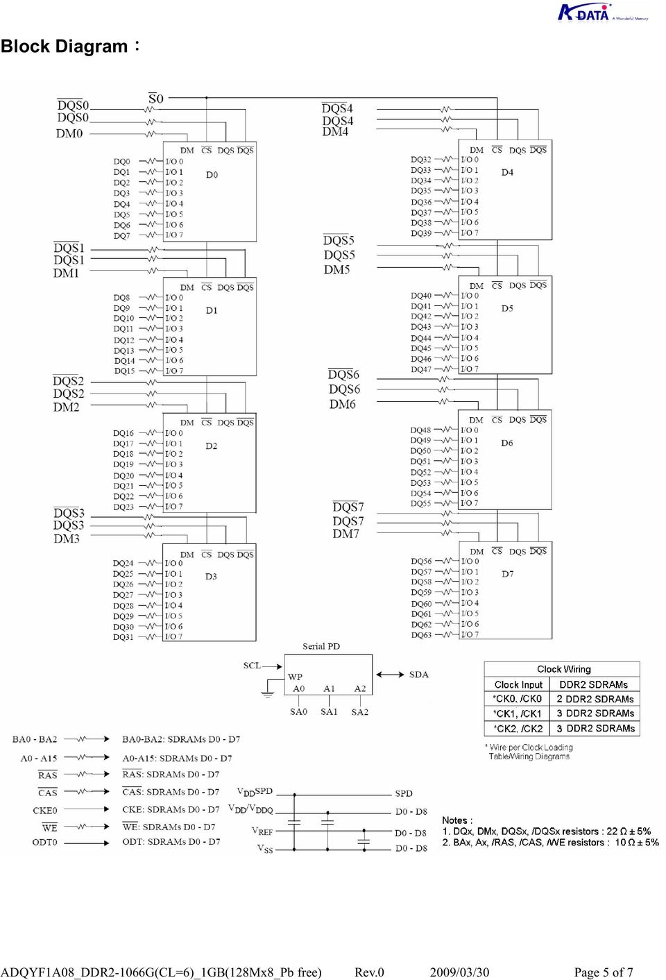
4 Block Diagram ADQYF1A08_DDR2-1066G(CL=6)_1GB(128Mx8_Pb free) Rev /03/30 Page 5 of 7
5 Absolute Maximum Ratings Parameter Symbol Value Unit Voltage on VDD supply relative to Vss VDD -1.0 ~ +2.3 V Voltage on VDDQ supply relative to Vss VDDQ -0.5 ~ +2.3 V Voltage on VDDL supply relative to Vss VDDQ -0.5 ~ +2.3 V Voltage on any pin relative to Vss VIN, Vout -0.5 ~ +2.3 V Storage temperature TSTG -55 ~ +100 Note: DDR2 SDRAM component specification. Operation Temperature Condition Parameter Symbol Value Unit Note DRAM Component Case Temperature Range TC 0~+95 1 Note: (1) If the DRAM case temperature is above 85 C, the Auto-Refresh command interval has to be reduced to trefi=3.9us. DC Operating Condition Voltage referenced to Vss = 0V, VDD&VDDQ=1.8V±0.1V, Tc = 0 to 85 Parameter Symbol Min Max Unit Note Supply Voltage VDD V 4,5 VDDSPD V Supply Voltage for DLL VDDL V 4 Supply Voltage for Output VDDQ V 4,5 Input Reference Voltage VREF 0.49 x VDDQ 0.51 x VDDQ V 1,2 Termination Voltage VTT VREF VREF V 3 Note: (1) There is no specific device VDD supply voltage requirement for SSTL_1.8 compliance. However under all conditions VDDQ must be less than or equal to VDD. (2) The value of VREF may be selected by the user to provide optimum noise margin in the system. Typically, the value of VREF is expected to be about 0.5 x VDDQ of the transmitting device and VREF is expected to track variations in VDDQ. (3) Peak to peak ac noise on VREF may not exceed +/- 2% VREF (ac). (4) VTT of transmitting device must track VREF of receiving device. (5) VDDQ tracks with VDD, VDDL tracks with VDD. AC parameters are measured with VDD, VDDQ and VDDL tied together. ADQYF1A08_DDR2-1066G(CL=6)_1GB(128Mx8_Pb free) Rev /03/30 Page 6 of 7

6 Package Dimensions ADQYF1A08_DDR2-1066G(CL=6)_1GB(128Mx8_Pb free) Rev /03/30 Page 7 of 7

ADATA Technology Corp. DDR3-1600(CL11) 240-Pin VLP ECC U-DIMM 4GB (512M x 72-bit)
 240-Pin VLP ECC U-DIMM 4GB (512M x 72-bit)") ADATA Technology Corp. Memory Module Data Sheet DDR3-1600(CL11) 240-Pin VLP ECC U-DIMM 4GB (512M x 72-bit) Version 0.1 Document Number : R11-0861 APPROVAL ISSUE Evan Sheu 2012/04/20 Masako Yang 2012/04/20
ADATA Technology Corp. Memory Module Data Sheet DDR3-1600(CL11) 240-Pin VLP ECC U-DIMM 4GB (512M x 72-bit) Version 0.1 Document Number : R11-0861 APPROVAL ISSUE Evan Sheu 2012/04/20 Masako Yang 2012/04/20
GR2DR4B-EXXX/YYY/LP 1GB & 2GB DDR2 REGISTERED DIMMs (LOW PROFILE)
") GENERAL DESCRIPTION The Gigaram is a 128M/256M bit x 72 DDDR2 SDRAM high density JEDEC standard ECC Registered memory module. The Gigaram consists of eighteen CMOS 128MX4 DDR2 for 1GB and thirty-six CMOS
GENERAL DESCRIPTION The Gigaram is a 128M/256M bit x 72 DDDR2 SDRAM high density JEDEC standard ECC Registered memory module. The Gigaram consists of eighteen CMOS 128MX4 DDR2 for 1GB and thirty-six CMOS
Features. DDR SODIMM Product Datasheet. Rev. 1.0 Oct. 2011
 Features 200pin, unbuffered small outline dual in-line memory module (SODIMM) Fast data transfer rates: PC-2100, PC-2700, PC3-3200 Single or Dual rank 256MB(32Megx64), 512MB (64Meg x 64), 1GB(128 Meg x
Jerry Chu 2010/07/07 Vincent Chang 2010/07/07
 Product Model Name: AD1S400A512M3 Product Specification: DDR-400(CL3) 200-Pin SO-DIMM 512MB (64M x 64-bits) Issuing Date: 2010/07/07 Version: 0 Item: 1. General Description 2. Features 3. Pin Assignment
Memory Module Specifications KVR667D2D4F5/4G. 4GB 512M x 72-Bit PC2-5300 CL5 ECC 240-Pin FBDIMM DESCRIPTION SPECIFICATIONS
 Memory Module Specifications KVR667DD4F5/4G 4GB 5M x 7-Bit PC-5300 CL5 ECC 40- FBDIMM DESCRIPTION This document describes s 4GB (5M x 7-bit) PC-5300 CL5 SDRAM (Synchronous DRAM) fully buffered ECC dual
Table 1: Address Table
 DDR SDRAM DIMM D32PB12C 512MB D32PB1GJ 1GB For the latest data sheet, please visit the Super Talent Electronics web site: www.supertalentmemory.com Features 184-pin, dual in-line memory module (DIMM) Fast
Memory Module Specifications KVR667D2D8F5/2GI. 2GB 256M x 72-Bit PC2-5300 CL5 ECC 240-Pin FBDIMM DESCRIPTION SPECIFICATIONS
 Memory Module Specifications KVR667DD8F5/GI GB 56M x 7-Bit PC-5300 CL5 ECC 40- FBDIMM DESCRIPTION This document describes s GB (56M x 7-bit) PC-5300 CL5 (Synchronous DRAM) fully buffered ECC dual rank,
Features. DDR3 Unbuffered DIMM Spec Sheet
 Features DDR3 functionality and operations supported as defined in the component data sheet 240-pin, unbuffered dual in-line memory module (UDIMM) Fast data transfer rates: PC3-8500, PC3-10600, PC3-12800
Features. DDR3 SODIMM Product Specification. Rev. 1.7 Feb. 2016
 Features DDR3 functionality and operations supported as defined in the component data sheet 204pin, small-outline dual in-line memory module (SODIMM) Fast data transfer rates: DDR3-1066(PC3-8500) DDR3-1333(PC3-10600)
DDR SDRAM SODIMM. MT9VDDT1672H 128MB 1 MT9VDDT3272H 256MB MT9VDDT6472H 512MB For component data sheets, refer to Micron s Web site: www.micron.
 Features DDR SDRAM SODIMM MT9VDDT1672H 128MB 1 MT9VDDT3272H 256MB MT9VDDT6472H 512MB For component data sheets, refer to Micron s Web site: www.micron.com Features 200-pin, small-outline dual in-line memory
DDR SDRAM UDIMM MT16VDDT6464A 512MB MT16VDDT12864A 1GB MT16VDDT25664A 2GB
 DDR SDRAM UDIMM MT16VDDT6464A 512MB MT16VDDT12864A 1GB MT16VDDT25664A 2GB For component data sheets, refer to Micron s Web site: www.micron.com 512MB, 1GB, 2GB (x64, DR) 184-Pin DDR SDRAM UDIMM Features
ADOVE1B163B2G. 1. General Description. 2. Features. 3. Pin Assignment. 4. Pin Description. 5. Block Diagram. 6. Absolute Maximum Ratings
 Product Model Name ADOVE1B163B2G Product Specification DDR2-800(CL6) 200-Pin SO-DIMM 2GB (256M x 64-bits) Issuing Date 2009/12/09 Version 0 Item 1. General Description 2. Features 3. Pin Assignment 4.
DDR SDRAM SODIMM. MT8VDDT3264H 256MB 1 MT8VDDT6464H 512MB For component data sheets, refer to Micron s Web site: www.micron.com
 SODIMM MT8VDDT3264H 256MB 1 MT8VDDT6464H 512MB For component data sheets, refer to Micron s Web site: www.micron.com 256MB, 512MB (x64, SR) 200-Pin SODIMM Features Features 200-pin, small-outline dual
are un-buffered 200-Pin Double Data Rate (DDR) Synchronous DRAM Small Outline Dual In-Line Memory Module (SO-DIMM). All devices
 Synchronous DRAM Small Outline Dual In-Line Memory Module (SO-DIMM). All devices") PC2700 200 pin Unbuffered DDR SO-DIMM Based on DDR333 512Mb bit B Die device Features 200-Pin Small Outline Dual In-Line Memory Module (SO-DIMM) Unbuffered DDR SO-DIMM based on 110nm 512M bit die B device,
PC2700 200 pin Unbuffered DDR SO-DIMM Based on DDR333 512Mb bit B Die device Features 200-Pin Small Outline Dual In-Line Memory Module (SO-DIMM) Unbuffered DDR SO-DIMM based on 110nm 512M bit die B device,
DDR SDRAM SODIMM MT16VDDF6464H 512MB MT16VDDF12864H 1GB
 SODIMM MT16VDDF6464H 512MB MT16VDDF12864H 1GB 512MB, 1GB (x64, DR) 200-Pin DDR SODIMM Features For component data sheets, refer to Micron s Web site: www.micron.com Features 200-pin, small-outline dual
DDR3(L) 4GB / 8GB UDIMM
 4GB / 8GB UDIMM") DRAM (512Mb x 8) DDR3(L) 4GB/8GB UDIMM DDR3(L) 4GB / 8GB UDIMM Features Nanya Technology Corp. DDR3(L) 4Gb B-Die JEDEC DDR3(L) Compliant 1-8n Prefetch Architecture - Differential Clock(CK/ ) and Data Strobe(/
DRAM (512Mb x 8) DDR3(L) 4GB/8GB UDIMM DDR3(L) 4GB / 8GB UDIMM Features Nanya Technology Corp. DDR3(L) 4Gb B-Die JEDEC DDR3(L) Compliant 1-8n Prefetch Architecture - Differential Clock(CK/ ) and Data Strobe(/
DDR2 SDRAM SODIMM MT16HTF12864H 1GB MT16HTF25664H 2GB
 Features DDR2 SDRAM SODIMM MT16HTF12864H 1GB MT16HTF25664H 2GB For component data sheets, refer to Micron s Web site: www.micron.com Features 200-pin, small outline dual in-line memory module (SODIMM)
DDR2 SDRAM SODIMM MT8HTF3264HD 256MB MT8HTF6464HD 512MB MT8HTF12864HD 1GB For component data sheets, refer to Micron s Web site: www.micron.
 DDR2 SDRAM SODIMM MT8HTF3264HD 256MB MT8HTF6464HD 512MB MT8HTF12864HD 1GB For component data sheets, refer to Micron s Web site: www.micron.com 256MB, 512MB, 1GB (x64, DR): 200-Pin DDR2 SODIMM Features
DDR3 SDRAM UDIMM MT8JTF12864A 1GB MT8JTF25664A 2GB
 DDR3 SDRAM UDIMM MT8JTF12864A 1GB MT8JTF25664A 2GB 1GB, 2GB (x64, SR) 240-Pin DDR3 SDRAM UDIMM Features For component data sheets, refer to Micron s Web site: www.micron.com Features DDR3 functionality
Address Summary Table: 128MB 256MB 512MB 1GB 2GB Module
 12MB - WD1SN12X0 256MB - WD1SN256X0 512MB - WD1SN512X0 1GB - WD1SN01GX0 2GB - WD1SN02GS0 (Stacked) Features: 200-pin Unbuffered Non-ECC DDR SDRAM SODIMM for DDR-266, DDR-333, DDR-400 JEDEC standard VDD=2.5V
Table 1 SDR to DDR Quick Reference
 TECHNICAL NOTE TN-6-05 GENERAL DDR SDRAM FUNCTIONALITY INTRODUCTION The migration from single rate synchronous DRAM (SDR) to double rate synchronous DRAM (DDR) memory is upon us. Although there are many
1.55V DDR2 SDRAM FBDIMM
 1.55V DDR2 SDRAM FBDIMM MT18RTF25672FDZ 2GB 2GB (x72, DR) 240-Pin DDR2 SDRAM FBDIMM Features Features 240-pin, fully buffered DIMM (FBDIMM) Very low-power DDR2 operation Component configuration: 256 Meg
DDR SDRAM Small-Outline DIMM MT16VDDF6464H 512MB MT16VDDF12864H 1GB
 Features DDR SDRAM Small-Outline DIMM MT16VDDF6464H 512MB MT16VDDF12864H 1GB For the latest component data sheet, refer to the Micron's Web site: www.micron.com/products/modules Features 200-pin, small-outline,
User s Manual HOW TO USE DDR SDRAM
 User s Manual HOW TO USE DDR SDRAM Document No. E0234E30 (Ver.3.0) Date Published April 2002 (K) Japan URL: http://www.elpida.com Elpida Memory, Inc. 2002 INTRODUCTION This manual is intended for users
V58C2512(804/404/164)SB HIGH PERFORMANCE 512 Mbit DDR SDRAM 4 BANKS X 16Mbit X 8 (804) 4 BANKS X 32Mbit X 4 (404) 4 BANKS X 8Mbit X 16 (164)
SB HIGH PERFORMANCE 512 Mbit DDR SDRAM 4 BANKS X 16Mbit X 8 (804) 4 BANKS X 32Mbit X 4 (404) 4 BANKS X 8Mbit X 16 (164)") V58C2512804/404/164SB HIGH PERFORMAE 512 Mbit DDR SDRAM 4 BANKS X 16Mbit X 8 804 4 BANKS X 32Mbit X 4 404 4 BANKS X 8Mbit X 16 164 5 6 75 DDR400 DDR333 DDR266 Clock Cycle Time t CK2.5 6ns 6ns 7.5ns Clock
V58C2512804/404/164SB HIGH PERFORMAE 512 Mbit DDR SDRAM 4 BANKS X 16Mbit X 8 804 4 BANKS X 32Mbit X 4 404 4 BANKS X 8Mbit X 16 164 5 6 75 DDR400 DDR333 DDR266 Clock Cycle Time t CK2.5 6ns 6ns 7.5ns Clock
Standard: 64M x 8 (9 components)
") 256MB - WD2RE256X09 512MB - WD2RE512X09 1GB - WD2RE01GX09 2GB - WD2RE02GH09 (Stacked, Preliminary*) DDR2-400, 533,667 One Rank, x Registered SDRAM DIMM Pb-free Features: 240-pin Registered ECC DDR2 SDRAM
256MB - WD2RE256X09 512MB - WD2RE512X09 1GB - WD2RE01GX09 2GB - WD2RE02GH09 (Stacked, Preliminary*) DDR2-400, 533,667 One Rank, x Registered SDRAM DIMM Pb-free Features: 240-pin Registered ECC DDR2 SDRAM
DOUBLE DATA RATE (DDR) SDRAM
 SDRAM") DOUBLE DATA RATE (DDR) SDRAM 256Mb: x8, x6 DDR 4 SDRAM Addendum MT46V32M8 8 MEG X 8 X 4 BANKS MT46V6M6 4 MEG X 6 X 4 BANKS For the latest data sheet revisions, please refer to the Micron Website: www.micron.com/dramds
DOUBLE DATA RATE (DDR) SDRAM 256Mb: x8, x6 DDR 4 SDRAM Addendum MT46V32M8 8 MEG X 8 X 4 BANKS MT46V6M6 4 MEG X 6 X 4 BANKS For the latest data sheet revisions, please refer to the Micron Website: www.micron.com/dramds
DDR2 SDRAM UDIMM MT18HTF6472AY 512MB MT18HTF12872AY 1GB MT18HTF25672AY 2GB MT18HTF51272AY 4GB. Features
 DDR SDRAM UDIMM MT8HTF647AY 5MB MT8HTF87AY GB MT8HTF567AY GB MT8HTF57AY 4GB 5MB, GB, GB, 4GB (x7, DR) 40-Pin DDR SDRAM UDIMM Features Features 40-pin, unbuffered dual in-line memory module Fast data transfer
DDR2 SDRAM Unbuffered DIMM MT9HTF3272A 256MB MT9HTF6472A 512MB MT9HTF12872A 1GB
 256MB, 52MB, GB (x72, SR, ECC) 24-Pin DDR2 SDRAM UDIMM Features DDR2 SDRAM Unbuffered DIMM MT9HTF3272A 256MB MT9HTF6472A 52MB MT9HTF2872A GB For the latest data sheet, please refer to the Micron Web site:
DDR2 SDRAM SODIMM MT8HTF12864HZ 1GB MT8HTF25664HZ 2GB. Features. 1GB, 2GB (x64, SR) 200-Pin DDR2 SDRAM SODIMM. Features
 200-Pin DDR2 SDRAM SODIMM. Features") DDR2 SDRAM SODIMM MT8HTF12864HZ 1GB MT8HTF25664HZ 2GB 1GB, 2GB (x64, SR) 200-Pin DDR2 SDRAM SODIMM Features Features 200-pin, small-outline dual in-line memory module (SODIMM) Fast data transfer rates:
DDR2 SDRAM SODIMM MT8HTF12864HZ 1GB MT8HTF25664HZ 2GB 1GB, 2GB (x64, SR) 200-Pin DDR2 SDRAM SODIMM Features Features 200-pin, small-outline dual in-line memory module (SODIMM) Fast data transfer rates:
Technical Note DDR2 Offers New Features and Functionality
 Technical Note DDR2 Offers New Features and Functionality TN-47-2 DDR2 Offers New Features/Functionality Introduction Introduction DDR2 SDRAM introduces features and functions that go beyond the DDR SDRAM
DDR2 SDRAM SODIMM MT8HTF6464HDZ 512MB MT8HTF12864HDZ 1GB. Features. 512MB, 1GB (x64, DR) 200-Pin DDR2 SODIMM. Features
 200-Pin DDR2 SODIMM. Features") DDR SDRAM SODIMM MT8HTF6464HDZ 5MB MT8HTF864HDZ GB 5MB, GB (x64, DR) 00-Pin DDR SODIMM Features Features 00-pin, small-outline dual in-line memory module (SODIMM) Fast data transfer rates: PC-300, PC-400,
DDR SDRAM SODIMM MT8HTF6464HDZ 5MB MT8HTF864HDZ GB 5MB, GB (x64, DR) 00-Pin DDR SODIMM Features Features 00-pin, small-outline dual in-line memory module (SODIMM) Fast data transfer rates: PC-300, PC-400,
Note: Data Rate (MT/s) CL = 3 CL = 4 CL = 5 CL = 6. t RCD (ns) t RP (ns) t RC (ns) t RFC (ns)
 CL = 3 CL = 4 CL = 5 CL = 6. t RCD (ns) t RP (ns) t RC (ns) t RFC (ns)") TwinDie DDR2 SDRAM MT47H512M4 32 Meg x 4 x 8 Banks x 2 Ranks MT47H256M8 16 Meg x 8 x 8 Banks x 2 Ranks 2Gb: x4, x8 TwinDie DDR2 SDRAM Features Features Uses two 1Gb Micron die Two ranks (includes dual
TwinDie DDR2 SDRAM MT47H512M4 32 Meg x 4 x 8 Banks x 2 Ranks MT47H256M8 16 Meg x 8 x 8 Banks x 2 Ranks 2Gb: x4, x8 TwinDie DDR2 SDRAM Features Features Uses two 1Gb Micron die Two ranks (includes dual
DDR2 SDRAM SODIMM MT16HTF12864HZ 1GB MT16HTF25664HZ 2GB MT16HTF51264HZ 4GB. Features. 1GB, 2GB, 4GB (x64, DR) 200-Pin DDR2 SDRAM SODIMM.
 200-Pin DDR2 SDRAM SODIMM.") DDR SDRAM SODIMM MT6HTF864HZ GB MT6HTF5664HZ GB MT6HTF564HZ 4GB GB, GB, 4GB (x64, DR) 00-Pin DDR SDRAM SODIMM Features Features 00-pin, small-outline dual in-line memory module (SODIMM) Fast data transfer
DDR SDRAM SODIMM MT6HTF864HZ GB MT6HTF5664HZ GB MT6HTF564HZ 4GB GB, GB, 4GB (x64, DR) 00-Pin DDR SDRAM SODIMM Features Features 00-pin, small-outline dual in-line memory module (SODIMM) Fast data transfer
DDR2 SDRAM SODIMM MT4HTF6464HZ 512MB. Features. 512MB (x64, SR) 200-Pin DDR2 SODIMM. Features. Figure 1: 200-Pin SODIMM (MO-224 R/C C)
 200-Pin DDR2 SODIMM. Features. Figure 1: 200-Pin SODIMM (MO-224 R/C C)") DDR2 SDRAM SODIMM MT4HTF6464HZ 512MB 512MB (x64, SR) 200-Pin DDR2 SODIMM Features Features 200-pin, small-outline dual in-line memory module (SODIMM) Fast data transfer rates: PC2-3200, PC2-4200, PC2-5300,
DDR2 SDRAM SODIMM MT4HTF6464HZ 512MB 512MB (x64, SR) 200-Pin DDR2 SODIMM Features Features 200-pin, small-outline dual in-line memory module (SODIMM) Fast data transfer rates: PC2-3200, PC2-4200, PC2-5300,
DDR SDRAM RDIMM MT36VDDF12872 1GB MT36VDDF25672 2GB
 DDR SDRAM RDIMM MT36VDDF12872 1GB MT36VDDF25672 2GB For component data sheets, refer to Micron s Web site: www.micron.com 1GB, 2GB (x72, ECC, DR) 184-Pin DDR SDRAM RDIMM Features Features 184-pin, registered
DDR2 SDRAM UDIMM MT16HTF6464AY 512MB MT16HTF12864AY 1GB MT16HTF25664AY 2GB MT16HTF51264AY 4GB. Features
 DDR SDRAM UDMM MT6HTF6464AY 5MB MT6HTF864AY GB MT6HTF5664AY GB MT6HTF564AY 4GB 5MB, GB, GB, 4GB (x64, DR) 40-Pin DDR UDMM Features Features 40-pin, unbuffered dual in-line memory module Fast data transfer
ThinkServer PC2-5300 DDR2 FBDIMM and PC2-6400 DDR2 SDRAM Memory options boost overall performance of ThinkServer solutions
 , dated September 30, 2008 ThinkServer PC2-5300 DDR2 FBDIMM and PC2-6400 DDR2 SDRAM Memory options boost overall performance of ThinkServer solutions Table of contents 2 Key prerequisites 2 Product number
JEDEC STANDARD DDR2 SDRAM SPECIFICATION JESD79-2B. (Revision of JESD79-2A) JEDEC SOLID STATE TECHNOLOGY ASSOCIATION. January 2005
 JEDEC SOLID STATE TECHNOLOGY ASSOCIATION. January 2005") JEDEC STANDARD DDR2 SDRAM SPECIFICATION JESD79-2B (Revision of JESD79-2A) January 2005 JEDEC SOLID STATE TECHNOLOGY ASSOCIATION NOTICE JEDEC standards and publications contain material that has been prepared,
JEDEC STANDARD DDR2 SDRAM SPECIFICATION JESD79-2B (Revision of JESD79-2A) January 2005 JEDEC SOLID STATE TECHNOLOGY ASSOCIATION NOTICE JEDEC standards and publications contain material that has been prepared,
Technical Note. Initialization Sequence for DDR SDRAM. Introduction. Initializing DDR SDRAM
 TN-46-8: Initialization Sequence for DDR SDRAM Introduction Technical Note Initialization Sequence for DDR SDRAM Introduction The double data rate DDR synchronous dynamic random access memory SDRAM device
DDR2 SDRAM SODIMM MT4HTF1664H 128MB MT4HTF3264H 256MB MT4HTF6464H 512MB
 Features DDR2 SDRAM SODIMM MT4HTF1664H 128MB MT4HTF3264H 256MB MT4HTF6464H 512MB For component specifications, refer to Micron s Web site: www.micron.com/products/ddr2sdram Features 200-pin, small outline,
DDR2 SDRAM FBDIMM MT9HTF6472F 512MB MT9HTF12872F 1GB. Features. 512MB, 1GB (x72, SR) 240-Pin DDR2 SDRAM FBDIMM. Features
 240-Pin DDR2 SDRAM FBDIMM. Features") SDRAM FBDIMM MT9HTF6472F 512MB MT9HTF12872F 1GB 512MB, 1GB (x72, SR) 240-Pin SDRAM FBDIMM Features Features 240-pin, fully buffered DIMM (FBDIMM) Fast data transfer rates: PC2-4200, PC2-5300, or PC2-6400
SDRAM FBDIMM MT9HTF6472F 512MB MT9HTF12872F 1GB 512MB, 1GB (x72, SR) 240-Pin SDRAM FBDIMM Features Features 240-pin, fully buffered DIMM (FBDIMM) Fast data transfer rates: PC2-4200, PC2-5300, or PC2-6400
DDR2 SDRAM FBDIMM MT36HTF25672F 2GB MT36HTF51272F 4GB. Features. 2GB, 4GB (x72, DR) 240-Pin DDR2 SDRAM FBDIMM. Features
 240-Pin DDR2 SDRAM FBDIMM. Features") SDRAM FBDIMM MT36HTF25672F 2GB MT36HTF51272F 4GB 2GB, 4GB (x72, DR) 240-Pin SDRAM FBDIMM Features Features 240-pin, fully buffered DIMM (FBDIMM) Fast data transfer rates: PC2-4200, PC2-5300, or PC2-6400
SDRAM FBDIMM MT36HTF25672F 2GB MT36HTF51272F 4GB 2GB, 4GB (x72, DR) 240-Pin SDRAM FBDIMM Features Features 240-pin, fully buffered DIMM (FBDIMM) Fast data transfer rates: PC2-4200, PC2-5300, or PC2-6400
3.11.5.5 DDR2 Specific SDRAM Functions
 JEDEC Standard No. 2-C Page..5.5..5.5 DDR2 Specific SDRAM Functions DDR2 SDRAM EMRS2 and EMRS For DDR2 SDRAMs, both bits BA and BA must be decoded for Mode/Extended Mode Register Set commands. Users must
DDR3 SDRAM UDIMM MT16JTF25664AZ 2GB MT16JTF51264AZ 4GB MT16JTF1G64AZ 8GB. Features. 2GB, 4GB, 8GB (x64, DR) 240-Pin DDR3 UDIMM.
 240-Pin DDR3 UDIMM.") DDR3 SDRAM UDIMM MT6JTF5664AZ GB MT6JTF564AZ 4GB MT6JTFG64AZ 8GB GB, 4GB, 8GB (x64, DR) 40-Pin DDR3 UDIMM Features Features DDR3 functionality and operations supported as per component data sheet 40-pin,
DDR3 SDRAM UDIMM MT6JTF5664AZ GB MT6JTF564AZ 4GB MT6JTFG64AZ 8GB GB, 4GB, 8GB (x64, DR) 40-Pin DDR3 UDIMM Features Features DDR3 functionality and operations supported as per component data sheet 40-pin,
DDR3 SDRAM SODIMM MT8JSF12864HZ 1GB MT8JSF25664HZ 2GB. Features. 1GB, 2GB (x64, SR) 204-Pin Halogen-Free DDR3 SDRAM SO- DIMM.
 204-Pin Halogen-Free DDR3 SDRAM SO- DIMM.") DDR3 SDRAM SO MT8JSF12864HZ 1GB MT8JSF25664HZ 2GB 1GB, 2GB (x64, SR) 204-Pin Halogen-Free DDR3 SDRAM SO- Features Features DDR3 functionality and operations supported as defined in the component data sheet
DDR3 SDRAM SO MT8JSF12864HZ 1GB MT8JSF25664HZ 2GB 1GB, 2GB (x64, SR) 204-Pin Halogen-Free DDR3 SDRAM SO- Features Features DDR3 functionality and operations supported as defined in the component data sheet
DDR2 SDRAM FBDIMM MT18HTF12872FD 1GB MT18HTF25672FD 2GB. Features. 1GB, 2GB (x72, DR) 240-Pin DDR2 SDRAM FBDIMM. Features
 240-Pin DDR2 SDRAM FBDIMM. Features") SDRAM FBDIMM MT18HTF12872FD 1GB MT18HTF25672FD 2GB 1GB, 2GB (x72, DR) 240-Pin SDRAM FBDIMM Features Features 240-pin, fully buffered dual in-line memory module (FBDIMM) Fast data transfer rates: PC2-4200,
SDRAM FBDIMM MT18HTF12872FD 1GB MT18HTF25672FD 2GB 1GB, 2GB (x72, DR) 240-Pin SDRAM FBDIMM Features Features 240-pin, fully buffered dual in-line memory module (FBDIMM) Fast data transfer rates: PC2-4200,
DDR3 SDRAM SODIMM MT16JSF25664HZ 2GB MT16JSF51264HZ 4GB. Features. 2GB, 4GB (x64, DR) 204-Pin Halogen-Free DDR3 SODIMM. Features
 204-Pin Halogen-Free DDR3 SODIMM. Features") DDR3 SDRAM SODIMM MT6JSF5664HZ GB MT6JSF564HZ 4GB GB, 4GB (x64, DR) 04-Pin Halogen-Free DDR3 SODIMM Features Features DDR3 functionality and operations supported as defined in the component data sheet
DDR3 SDRAM SODIMM MT6JSF5664HZ GB MT6JSF564HZ 4GB GB, 4GB (x64, DR) 04-Pin Halogen-Free DDR3 SODIMM Features Features DDR3 functionality and operations supported as defined in the component data sheet
DDR SDRAM UNBUFFERED DIMM
 DDR SDRAM UNBUFFERED DIMM Features 84-pin, dual in-line memory module (DIMM) Fast data transfer rates: PC2 or PC27 Utilizes 266 MT/s and 333 MT/s DDR SDRAM components 256MB (32 Meg x 64), 52MB (64 Meg
DDR2 VLP-Registered DIMM Module
 DDR2 VLP-Registered DIMM Module 256MB based on 256Mbit component 512MB, 1GB based on 512Mbit component 1GB, 2GB, 4GB based on 1Gbit component ATCA Compliant 60 Balls FBGA with Pb-Free Revision 1.0 (Mar.
DDR2 Device Operations & Timing Diagram DDR2 SDRAM. Device Operations & Timing Diagram
 DDR2 SDRAM Device Operations & Timing Diagram 1 Contents 1. Functional Description 1.1 Simplified State Diagram 1.2 Basic Function & Operation of DDR2 SDRAM 1.2.1 Power up and Initialization 1.2.2 Programming
White Paper David Hibler Jr Platform Solutions Engineer Intel Corporation. Considerations for designing an Embedded IA System with DDR3 ECC SO-DIMMs
 White Paper David Hibler Jr Platform Solutions Engineer Intel Corporation Considerations for designing an Embedded IA System with DDR3 ECC SO-DIMMs September 2012 326491 Executive Summary What are ECC
2GB DDR2 SDRAM SO-DIMM
 2GB DDR2 SDRAM SO-DIMM 200 Pin SO-DIMM SEN02G64C4BF2SA-25R 2GB PC2-5300 in FBGA Technoloy RoHS compliant Options: Frequency / Latency Marking DDR2 800 MT/s CL6-25 DDR2 667 MT/s CL5-30 DDR2 533 MT/s CL4-37
DDR2 Unbuffered SDRAM MODULE
 DDR2 Unbuffered SDRAM MODULE 240pin Unbuffered Module based on 1Gb Q-die 64/72-bit Non-ECC/ECC 60FBGA & 84FBGA with Lead-Free and Halogen-Free (RoHS compliant) INFORMATION IN THIS DOCUMENT IS PROVIDED
A N. O N Output/Input-output connection
 Memory Types Two basic types: ROM: Read-only memory RAM: Read-Write memory Four commonly used memories: ROM Flash, EEPROM Static RAM (SRAM) Dynamic RAM (DRAM), SDRAM, RAMBUS, DDR RAM Generic pin configuration:
DDR3 SDRAM SODIMM MT8JSF25664HDZ 2GB. Features. 2GB (x64, DR) 204-Pin DDR3 SODIMM. Features. Figure 1: 204-Pin SODIMM (MO-268 R/C A)
 204-Pin DDR3 SODIMM. Features. Figure 1: 204-Pin SODIMM (MO-268 R/C A)") DDR3 SDRAM SODIMM MT8JSF5664HDZ GB GB (x64, DR) 04-Pin DDR3 SODIMM Features Features DDR3 functionality and operations supported as defined in the component data sheet 04-pin, small-outline dual in-line
DDR3 SDRAM SODIMM MT8JSF5664HDZ GB GB (x64, DR) 04-Pin DDR3 SODIMM Features Features DDR3 functionality and operations supported as defined in the component data sheet 04-pin, small-outline dual in-line
Dual DIMM DDR2 and DDR3 SDRAM Interface Design Guidelines
 Dual DIMM DDR2 and DDR3 SDRAM Interface Design Guidelines May 2009 AN-444-1.1 This application note describes guidelines for implementing dual unbuffered DIMM DDR2 and DDR3 SDRAM interfaces. This application
Mobile SDRAM. MT48H16M16LF 4 Meg x 16 x 4 banks MT48H8M32LF 2 Meg x 32 x 4 banks
 Features Mobile SDRAM MT48H6M6LF 4 Meg x 6 x 4 banks MT48H8M32LF 2 Meg x 32 x 4 banks Features Fully synchronous; all signals registered on positive edge of system clock V DD /V D =.7.95V Internal, pipelined
IS42/45R86400D/16320D/32160D IS42/45S86400D/16320D/32160D
 IS42/45R86400D/16320D/32160D IS42/45S86400D/16320D/32160D 16Mx32, 32Mx16, 64Mx8 512Mb SDRAM FEATURES Clock frequency: 200, 166, 143 MHz Fully synchronous; all signals referenced to a positive clock edge
DDR SDRAM UNBUFFERED DIMM
 DDR SDRAM UNBUFFERED DIMM 28MB, 256MB, 52MB (x72, ECC, SR), PC32 84-Pin DDR SDRAM UDIMM MT9VDDT672A 28MB MT9VDDT3272A 256MB MT9VDDT6472A 52MB For the latest data sheet, please refer to the Micron Web site:
512MB DDR SDRAM SoDIMM
 512MB DDR SDRAM SoDIMM 200 PIN SO-DIMM SDN06464D1BJ1SA-xx(W)R 512MByte in FBGA Technology RoHS compliant Options: Data Rate / Latency Marking DDR 400 MT/s CL3-50 DDR 333 MT/s CL2.5-60 Module density 512MB
NTE2053 Integrated Circuit 8 Bit MPU Compatible A/D Converter
 NTE2053 Integrated Circuit 8 Bit MPU Compatible A/D Converter Description: The NTE2053 is a CMOS 8 bit successive approximation Analog to Digital converter in a 20 Lead DIP type package which uses a differential
REV 1.2 1 03/2007 NANYA TECHNOLOGY CORP. NANYA TECHNOLOGY CORP. reserves the right to change Products and Specifications without notice.
 240pin Unbuffered DDR2 SDRAM MODULE Based on 64Mx8 & 32Mx16 DDR2 SDRAM B Die Features Performance: Speed Sort PC2-4200 PC2-5300 PC2-6400 PC2-6400 -37B -3C -25D -25C DIMM Latency * 4 5 6 5 f CK Clock Frequency
Fairchild Solutions for 133MHz Buffered Memory Modules
 AN-5009 Fairchild Semiconductor Application Note April 1999 Revised December 2000 Fairchild Solutions for 133MHz Buffered Memory Modules Fairchild Semiconductor provides several products that are compatible
JEDEC STANDARD. Double Data Rate (DDR) SDRAM Specification JESD79C. (Revision of JESD79B) JEDEC SOLID STATE TECHNOLOGY ASSOCIATION MARCH 2003
 SDRAM Specification JESD79C. (Revision of JESD79B) JEDEC SOLID STATE TECHNOLOGY ASSOCIATION MARCH 2003") JEDEC STANDARD Double Data Rate (DDR) SDRAM Specification JESD79C (Revision of JESD79B) MARCH 2003 JEDEC SOLID STATE TECHNOLOGY ASSOCIATION NOTICE JEDEC standards and publications contain material that
JEDEC STANDARD Double Data Rate (DDR) SDRAM Specification JESD79C (Revision of JESD79B) MARCH 2003 JEDEC SOLID STATE TECHNOLOGY ASSOCIATION NOTICE JEDEC standards and publications contain material that
DDR2 SDRAM Registered MiniDIMM MT9HTF3272(P)K 256MB MT9HTF6472(P)K 512MB MT9HTF12872(P)K 1GB
K 256MB MT9HTF6472(P)K 512MB MT9HTF12872(P)K 1GB") Features DDR2 SDRAM Registered MiniDIMM MT9HTF3272(P)K 256MB MT9HTF6472(P)K 512MB MT9HTF172(P)K 1GB For component specifications, refer to Micron s Web site: www.micron.com/products/dram/ddr2 Features
Features DDR2 SDRAM Registered MiniDIMM MT9HTF3272(P)K 256MB MT9HTF6472(P)K 512MB MT9HTF172(P)K 1GB For component specifications, refer to Micron s Web site: www.micron.com/products/dram/ddr2 Features
Parity 3. Data Rate (MT/s) CL = 6 CL = 5 CL = 4 CL = 3-80E PC2-6400 800 533 12.5 12.5 55
 CL = 6 CL = 5 CL = 4 CL = 3-80E PC2-6400 800 533 12.5 12.5 55") Features DDR2 SDRAM Registered DIMM (RDIMM) MT18HTF6472 512MB MT18HTF12872(P) 1GB MT18HTF25672(P) 2GB For component data sheets, refer to Micron's Web site: www.micron.com Features 240-pin, registered
Features DDR2 SDRAM Registered DIMM (RDIMM) MT18HTF6472 512MB MT18HTF12872(P) 1GB MT18HTF25672(P) 2GB For component data sheets, refer to Micron's Web site: www.micron.com Features 240-pin, registered
Tuning DDR4 for Power and Performance. Mike Micheletti Product Manager Teledyne LeCroy
 Tuning DDR4 for Power and Performance Mike Micheletti Product Manager Teledyne LeCroy Agenda Introduction DDR4 Technology Expanded role of MRS Power Features Examined Reliability Features Examined Performance
Tuning DDR4 for Power and Performance. Mike Micheletti Product Manager Teledyne LeCroy
 Tuning DDR4 for Power and Performance Mike Micheletti Product Manager Teledyne LeCroy Agenda Introduction DDR4 Technology Expanded role of MRS Power Features Examined Reliability Features Examined Performance
Feature. CAS Latency Frequency. trcd 15-12.5-11.25 - ns. trp 15-12.5-11.25 - ns. trc 60-57.5-56.25 - ns. tras 45 70K 45 70K 45 70K ns
 Feature CAS Latency Frequency DDR2-667 DDR2-8 DDR2-66 Speed Sorts -3C -AC -BD Units (CL-tRCD-tRP) 5-5-5 5-5-5 6-6-6 Parameter min max min max min max tck(avg.) Max. Clock Frequency 25 333 25 4 25 533 MHz
DDR SDRAM Memory Termination USING THE LX1672 AND LX1673 FOR DDR SDRAM MEMORY TERMINATION INTEGRATED PRODUCTS. Microsemi
 AN-17 USING THE LX1672 AND LX1673 FOR DDR SDRAM MEMORY TERMINATION LX1672 Protected by US Patents: 6,285,571 & 6,292,378 INTEGRATED PRODUCTS Page 1 TABLE OF CONTENTS 1.0 INTRODUCTION... 3 2.0 SDR vs DDR
PT973216BG. 32M x 4BANKS x 16BITS DDRII. Table of Content-
 PT973216BG 32M x 4BANKS x 16BITS DDRII Table of Content- 1. FEATURES......... 3 2. Description...4 3. Pi n Confi gur ation............. 5 4. TFBGA Ball Out Diagrams......9 5. Block Diagrams...12 6. FUNCTIONAL
Application Note for General PCB Design Guidelines for Mobile DRAM
 SEC-Mobile-UtRAM Application Note for General PCB Design Guidelines for Mobile DRAM Version 1.0, May 2009 Samsung Electronics Copyright c 2009 Samsung Electronics Co., LTD. Copyright 2009 Samsung Electronics
DDR3 DIMM Slot Interposer
 DDR3 DIMM Slot Interposer DDR3-1867 Digital Validation High Speed DDR3 Digital Validation Passive 240-pin DIMM Slot Interposer Custom Designed for Agilent Logic Analyzers Compatible with Agilent Software
White Paper Utilizing Leveling Techniques in DDR3 SDRAM Memory Interfaces
 White Paper Introduction The DDR3 SDRAM memory architectures support higher bandwidths with bus rates of 600 Mbps to 1.6 Gbps (300 to 800 MHz), 1.5V operation for lower power, and higher densities of 2
DS1225Y 64k Nonvolatile SRAM
 DS1225Y 64k Nonvolatile SRAM www.maxim-ic.com FEATURES years minimum data retention in the absence of external power Data is automatically protected during power loss Directly replaces 2k x 8 volatile
Features. Dimensions
 Description With an IDE interface and strong data retention ability, 40-Pin IDE Flash Modules are ideal for use in the harsh environments where Industrial PCs, Set-Top Boxes, etc. are used. Placement Features
4M x 16Bits x 4Banks Mobile Synchronous DRAM
 4M x 16Bits x 4Banks Mobile Synchronous DRAM Description These IS42/45SM/RM/VM16160K are mobile 268,435,456 bits CMOS Synchronous DRAM organized as 4 banks of 4,194,304 words x 16 bits. These products
Product Specification. RoHS-6 Compliant 10Gb/s 850nm Multimode Datacom XFP Optical Transceiver FTLX8512D3BCL
 Product Specification RoHS-6 Compliant 10Gb/s 850nm Multimode Datacom XFP Optical Transceiver FTLX8512D3BCL PRODUCT FEATURES Hot-pluggable XFP footprint Supports 8.5Gb/s and 9.95 through 10.5Gb/s* bit
Technical Note DDR3 ZQ Calibration
 Introduction Technical Note DDR3 ZQ Calibration Introduction For more robust system operation, the DDR3 SDRAM driver design has been enhanced with reduced capacitance, dynamic on-die termination (ODT),
Computer Architecture
 Computer Architecture Random Access Memory Technologies 2015. április 2. Budapest Gábor Horváth associate professor BUTE Dept. Of Networked Systems and Services [email protected] 2 Storing data Possible
TRIPLE PLL FIELD PROG. SPREAD SPECTRUM CLOCK SYNTHESIZER. Features
 DATASHEET ICS280 Description The ICS280 field programmable spread spectrum clock synthesizer generates up to four high-quality, high-frequency clock outputs including multiple reference clocks from a low-frequency
Features. Dimensions
 Description With an IDE interface and strong data retention ability, 40-Pin IDE Flash Modules are ideal for use in the harsh environments where Industrial PCs, Set-Top Boxes, etc. are used. Placement Features
Features. Dimensions
 Description With an IDE interface and strong data retention ability, 44-Pin IDE Flash Modules are ideal for use in the harsh environments where Industrial PCs, Set-Top Boxes, etc. are used. Placement Features
1M x 32 Bit x 4 Banks Synchronous DRAM
 SDRAM FEATURES JEDEC standard 3.3V power supply LVTTL compatible with multiplexed address Four banks operation MRS cycle with address key programs - Latency (1, 2 & 3 ) - Burst Length ( 1, 2, 4, 8 & full
11. High-Speed Differential Interfaces in Cyclone II Devices
 11. High-Speed Differential Interfaces in Cyclone II Devices CII51011-2.2 Introduction From high-speed backplane applications to high-end switch boxes, low-voltage differential signaling (LVDS) is the
DDR subsystem: Enhancing System Reliability and Yield
 DDR subsystem: Enhancing System Reliability and Yield Agenda Evolution of DDR SDRAM standards What is the variation problem? How DRAM standards tackle system variability What problems have been adequately
RealSSD Embedded USB Mass Storage Drive MTFDCAE001SAF, MTFDCAE002SAF, MTFDCAE004SAF, MTFDCAE008SAF
 RealSSD Embedded USB Mass Storage Drive MTFDCAE001SAF, MTFDCAE002SAF, MTFDCAE004SAF, MTFDCAE008SAF Embedded USB Mass Storage Drive Features Features Micron NAND Flash Interface: Universal Serial Bus (USB)
SOLVING HIGH-SPEED MEMORY INTERFACE CHALLENGES WITH LOW-COST FPGAS
 SOLVING HIGH-SPEED MEMORY INTERFACE CHALLENGES WITH LOW-COST FPGAS A Lattice Semiconductor White Paper May 2005 Lattice Semiconductor 5555 Northeast Moore Ct. Hillsboro, Oregon 97124 USA Telephone: (503)
Semiconductor Device Technology for Implementing System Solutions: Memory Modules
 Hitachi Review Vol. 47 (1998), No. 4 141 Semiconductor Device Technology for Implementing System Solutions: Memory Modules Toshio Sugano Atsushi Hiraishi Shin ichi Ikenaga ABSTRACT: New technology is producing
1-Mbit (128K x 8) Static RAM
 Static RAM") 1-Mbit (128K x 8) Static RAM Features Pin- and function-compatible with CY7C109B/CY7C1009B High speed t AA = 10 ns Low active power I CC = 80 ma @ 10 ns Low CMOS standby power I SB2 = 3 ma 2.0V Data Retention
1-Mbit (128K x 8) Static RAM Features Pin- and function-compatible with CY7C109B/CY7C1009B High speed t AA = 10 ns Low active power I CC = 80 ma @ 10 ns Low CMOS standby power I SB2 = 3 ma 2.0V Data Retention
DDR2 SDRAM FBDIMM MT18HTF12872F 1GB MT18HTF25672F 2GB
 SDRAM FBDIMM MT18HTF12872F 1GB MT18HTF25672F 2GB 1GB, 2GB (x72, SR) 240-Pin SDRAM FBDIMM Features For the latest data sheets and technical notes, refer to Micron s Web site: www.micron.com Features 240-pin,
Features. Modulation Frequency (khz) VDD. PLL Clock Synthesizer with Spread Spectrum Circuitry GND
 VDD. PLL Clock Synthesizer with Spread Spectrum Circuitry GND") DATASHEET IDT5P50901/2/3/4 Description The IDT5P50901/2/3/4 is a family of 1.8V low power, spread spectrum clock generators capable of reducing EMI radiation from an input clock. Spread spectrum technique
DATASHEET IDT5P50901/2/3/4 Description The IDT5P50901/2/3/4 is a family of 1.8V low power, spread spectrum clock generators capable of reducing EMI radiation from an input clock. Spread spectrum technique