Status of the design of the TDC for the GTK TDCpix ASIC
|
|
|
- Brett Cooper
- 8 years ago
- Views:
Transcription
1 Status of the design of the TDC for the GTK TDCpix ASIC Gianluca Aglieri Rinella, Lukas Perktold DLL design review meeting,

2 Outline Introduction Purpose and objectives Reminder Challenges of design TDC Block diagram and description Status of design Routing of code lines Power distribution

3 Objectives and purpose of this review Check verification methodologies Aspects that might still be overlooked Formal approval by experts of the DLL circuit DLL believed to be finished

4 Reminder of circuit requirements v [au] t [s] Discriminator Hit leading Hit falling 320 MHz ns n-3 n-2 n-1 n n+1 n+2 n+3 Coarse code

5 Challenges of design TDC design tested in the prototype DLL + fine and coarse time stamp registers DLL re-design challenges Detailed by Lukas Fine and coarse registers re-design Parallel readout and 32 to 5 bit encoding of fine codes Reduction of bits of coarse counters Layout Combine DLL, fine code registers and encoders Fit inside the width of one pixel column (300 um) Routing

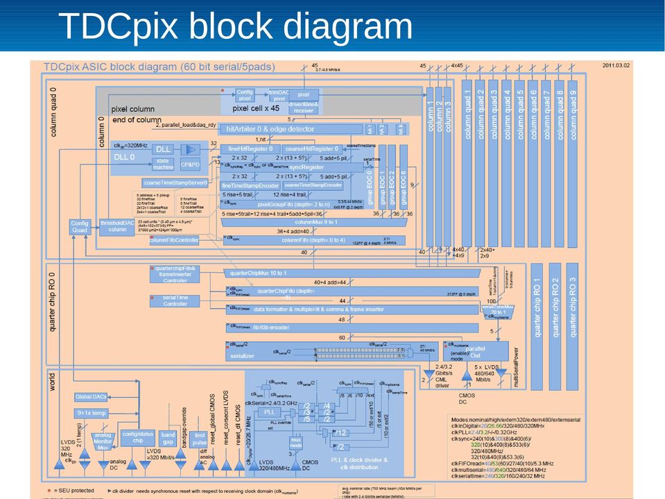
6 TDCpix block diagram

7 TDCpix block diagram - TDC

8 TDC block diagram x9 Hit Hit arbiter + Hit arbiter Hit arbiter RO control TDC DLL 32 x9 FIFO write FIFO full x9 Coarse register (rise) Coarse Coarse counter Pixelgroup group Pixel Pixel group FIFO FIFO FIFO x9


9 DLL and fine code registers DLL Block diagram Buffers Buffers 32 Floor plan

10 Layout fits column width DLL Buffers Buffers 32

11 Status of DLL DLL (Lukas) Fully characterized Detail documentation State machine Being transferred from the prototype design

12 Fine time stamp registers Existing 32b registers modified No changes to custom building cells (buffers and FFs) Added parallel outputs to layout Layout of power stripes Added explicit sub pins (no use of global nets) Added gate tie downs
 Added gate tie")
13 Time stamp 32to5 encoder block Synthesized from HDL with SoCEncounter, imported into Virtuoso

14 Edge Detector Edge Detector Modification of block from prototype asic One input only, buffering stages added Layout modifications Some of original buffer cells from Sakari have been modified (more compact layout) Option to replace this block with simple repeaters being considered
 Option to replace this block with simple repeaters being")
15 Buffers for DLL wires Buffers DLL fine code lines repeaters Design and characterization by Lukas 32x double inverters Details in Lukas presentation

16 Buffers on DLL wires DLL buffers Buffers Buffers Placed at 1/3 and 2/3 of registers bank height, i.e. wires length

17 Routing of DLL fine code wires Fine code lines Pitch adpater Bias decoupling capacitor 32b Register 32to5 A A' MG Vhigh / vlow Cross section AA' Enc<m-1> vlow vlow DLL<n> vhigh vhigh Enc<m> Enc<m+1> Enc<m+2> Vlow / vhigh / Register circuits vlow vlow DLL<n+1> MQ M3

18 Powering scheme Dedicated power domain for DLL Fine hit registers s Buffers (code repeaters) Edge detectors (hit repeaters) Substrate isolation DLL in a substrate area surrounded by high resistivity undoped region Register bank also isolated Decoupling capacitors

19 Powering scheme diagram BFMOAT vhigh SubDll DLL DLL vlow 11 pf SubReg Fine Fine Fine 11 pf Fine Fine Fine Buffers Buffers Fine Fine Fine Fine Fine Fine Buffers Buffers vhigh Fine Fine Fine Fine Fine Fine vlow 11 pf 11 pf

20 Summary of TDC status Done DLL Fine timestamp registers, s, Edge detectors Routing of DLL lines Interconnection bus To do Replace edge detectors with repeaters Route transmission line for DLL input clock Coarse code generator and registers See concept design by Gianluca Functional and timing models for all blocks Global verification

21 Spare slides
22 DM 3-2 MA / E / Global signals (clk, reset) Ver Hor Power stripes LY / Local routing MG / MQ / M3 M2 M / / / Power stripes Ver Hor Regional routing Local routing Ver Hor Ver Hor
23 Voltage drop on power rails Model including Inductance of bonding wires Input impedance of DLL Resistance and capacitance of minimum size powering stripes Worst case pessimistic assumptions for all estimates and stimulus Decoupling capacitors have sizable effect WITHOUT decoupling capacitors WITH decoupling capacitors
Alpha CPU and Clock Design Evolution
 Alpha CPU and Clock Design Evolution This lecture uses two papers that discuss the evolution of the Alpha CPU and clocking strategy over three CPU generations Gronowski, Paul E., et.al., High Performance
PLAS: Analog memory ASIC Conceptual design & development status
 PLAS: Analog memory ASIC Conceptual design & development status Ramón J. Aliaga Instituto de Física Corpuscular (IFIC) Consejo Superior de Investigaciones Científicas (CSIC) Universidad de Valencia Vicente
Fairchild Solutions for 133MHz Buffered Memory Modules
 AN-5009 Fairchild Semiconductor Application Note April 1999 Revised December 2000 Fairchild Solutions for 133MHz Buffered Memory Modules Fairchild Semiconductor provides several products that are compatible
Reconfigurable ECO Cells for Timing Closure and IR Drop Minimization. TingTing Hwang Tsing Hua University, Hsin-Chu
 Reconfigurable ECO Cells for Timing Closure and IR Drop Minimization TingTing Hwang Tsing Hua University, Hsin-Chu 1 Outline Introduction Engineering Change Order (ECO) Voltage drop (IR-DROP) New design
NTE2053 Integrated Circuit 8 Bit MPU Compatible A/D Converter
 NTE2053 Integrated Circuit 8 Bit MPU Compatible A/D Converter Description: The NTE2053 is a CMOS 8 bit successive approximation Analog to Digital converter in a 20 Lead DIP type package which uses a differential
Status of CBM-XYTER Development
 Status of CBM-XYTER Development Latest Results of the CSA/ADC Test-Chip Tim Armbruster tim.armbruster@ziti.uni-heidelberg.de Heidelberg University Schaltungstechnik Schaltungstechnik und und 14th CBM CM
Lab #5: Design Example: Keypad Scanner and Encoder - Part 1 (120 pts)
") Dr. Greg Tumbush, gtumbush@uccs.edu Lab #5: Design Example: Keypad Scanner and Encoder - Part 1 (120 pts) Objective The objective of lab assignments 5 through 9 are to systematically design and implement
Dr. Greg Tumbush, gtumbush@uccs.edu Lab #5: Design Example: Keypad Scanner and Encoder - Part 1 (120 pts) Objective The objective of lab assignments 5 through 9 are to systematically design and implement
Signal Integrity: Tips and Tricks
 White Paper: Virtex-II, Virtex-4, Virtex-5, and Spartan-3 FPGAs R WP323 (v1.0) March 28, 2008 Signal Integrity: Tips and Tricks By: Austin Lesea Signal integrity (SI) engineering has become a necessary
ANN Based Modeling of High Speed IC Interconnects. Q.J. Zhang, Carleton University
 ANN Based Modeling of High Speed IC Interconnects Needs for Repeated Simulation Signal integrity optimization Iterative design and re-optimization Monte-Carlo analysis Yield optimization Iterative design
Application Note AN:005. FPA Printed Circuit Board Layout Guidelines. Introduction Contents. The Importance of Board Layout
 FPA Printed Circuit Board Layout Guidelines By Paul Yeaman Principal Product Line Engineer V I Chip Strategic Accounts Introduction Contents Page Introduction 1 The Importance of 1 Board Layout Low DC
Clocking. Figure by MIT OCW. 6.884 - Spring 2005 2/18/05 L06 Clocks 1
 ing Figure by MIT OCW. 6.884 - Spring 2005 2/18/05 L06 s 1 Why s and Storage Elements? Inputs Combinational Logic Outputs Want to reuse combinational logic from cycle to cycle 6.884 - Spring 2005 2/18/05
Module 7 : I/O PADs Lecture 33 : I/O PADs
 Module 7 : I/O PADs Lecture 33 : I/O PADs Objectives In this lecture you will learn the following Introduction Electrostatic Discharge Output Buffer Tri-state Output Circuit Latch-Up Prevention of Latch-Up
EE 42/100 Lecture 24: Latches and Flip Flops. Rev B 4/21/2010 (2:04 PM) Prof. Ali M. Niknejad
 Prof. Ali M. Niknejad") A. M. Niknejad University of California, Berkeley EE 100 / 42 Lecture 24 p. 1/20 EE 42/100 Lecture 24: Latches and Flip Flops ELECTRONICS Rev B 4/21/2010 (2:04 PM) Prof. Ali M. Niknejad University of California,
A. M. Niknejad University of California, Berkeley EE 100 / 42 Lecture 24 p. 1/20 EE 42/100 Lecture 24: Latches and Flip Flops ELECTRONICS Rev B 4/21/2010 (2:04 PM) Prof. Ali M. Niknejad University of California,
PL-277x Series SuperSpeed USB 3.0 SATA Bridge Controllers PCB Layout Guide
 Application Note PL-277x Series SuperSpeed USB 3.0 SATA Bridge Controllers PCB Layout Guide Introduction This document explains how to design a PCB with Prolific PL-277x SuperSpeed USB 3.0 SATA Bridge
A Lesson on Digital Clocks, One Shots and Counters
 A Lesson on Digital Clocks, One Shots and Counters Topics Clocks & Oscillators LM 555 Timer IC Crystal Oscillators Selection of Variable Resistors Schmitt Gates Power-On Reset Circuits One Shots Counters
How To Design A Chip Layout
 Spezielle Anwendungen des VLSI Entwurfs Applied VLSI design (IEF170) Course and contest Intermediate meeting 3 Prof. Dirk Timmermann, Claas Cornelius, Hagen Sämrow, Andreas Tockhorn, Philipp Gorski, Martin
A Lesson on Digital Clocks, One Shots and Counters
 A Lesson on Digital Clocks, One Shots and Counters Topics Clocks & Oscillators LM 555 Timer IC Crystal Oscillators Selection of Variable Resistors Schmitt Gates Power-On Reset Circuits One Shots Counters
SPADIC: CBM TRD Readout ASIC
 SPADIC: CBM TRD Readout ASIC Tim Armbruster tim.armbruster@ziti.uni-heidelberg.de HIC for FAIR, Darmstadt Schaltungstechnik Schaltungstechnik und und February 2011 Visit http://spadic.uni-hd.de 1. Introduction
DS2187 Receive Line Interface
 Receive Line Interface www.dalsemi.com FEATURES Line interface for T1 (1.544 MHz) and CEPT (2.048 MHz) primary rate networks Extracts clock and data from twisted pair or coax Meets requirements of PUB
DM9368 7-Segment Decoder/Driver/Latch with Constant Current Source Outputs
 DM9368 7-Segment Decoder/Driver/Latch with Constant Current Source Outputs General Description The DM9368 is a 7-segment decoder driver incorporating input latches and constant current output circuits
Chapter 6: From Digital-to-Analog and Back Again
 Chapter 6: From Digital-to-Analog and Back Again Overview Often the information you want to capture in an experiment originates in the laboratory as an analog voltage or a current. Sometimes you want to
User s Manual HOW TO USE DDR SDRAM
 User s Manual HOW TO USE DDR SDRAM Document No. E0234E30 (Ver.3.0) Date Published April 2002 (K) Japan URL: http://www.elpida.com Elpida Memory, Inc. 2002 INTRODUCTION This manual is intended for users
Digital to Analog Converter. Raghu Tumati
 Digital to Analog Converter Raghu Tumati May 11, 2006 Contents 1) Introduction............................... 3 2) DAC types................................... 4 3) DAC Presented.............................
VJ 6040 Mobile Digital TV UHF Antenna Evaluation Board
 VISHAY VITRAMON Multilayer Chip Capacitors Application Note GENERAL is a multilayer ceramic chip antenna designed for receiving mobile digital TV transmissions in the UHF band. The target application for
11. High-Speed Differential Interfaces in Cyclone II Devices
 11. High-Speed Differential Interfaces in Cyclone II Devices CII51011-2.2 Introduction From high-speed backplane applications to high-end switch boxes, low-voltage differential signaling (LVDS) is the
TSL213 64 1 INTEGRATED OPTO SENSOR
 TSL 64 INTEGRATED OPTO SENSOR SOES009A D4059, NOVEMBER 99 REVISED AUGUST 99 Contains 64-Bit Static Shift Register Contains Analog Buffer With Sample and Hold for Analog Output Over Full Clock Period Single-Supply
Features. Modulation Frequency (khz) VDD. PLL Clock Synthesizer with Spread Spectrum Circuitry GND
 VDD. PLL Clock Synthesizer with Spread Spectrum Circuitry GND") DATASHEET IDT5P50901/2/3/4 Description The IDT5P50901/2/3/4 is a family of 1.8V low power, spread spectrum clock generators capable of reducing EMI radiation from an input clock. Spread spectrum technique
DATASHEET IDT5P50901/2/3/4 Description The IDT5P50901/2/3/4 is a family of 1.8V low power, spread spectrum clock generators capable of reducing EMI radiation from an input clock. Spread spectrum technique
CHAPTER 11: Flip Flops
 CHAPTER 11: Flip Flops In this chapter, you will be building the part of the circuit that controls the command sequencing. The required circuit must operate the counter and the memory chip. When the teach
Product Specification PE9304
 PE9304 Product Description The PE9304 is a high-performance UltraCMOS prescaler with a fixed divide ratio of 2. Its operating frequency range is 1000 7000 MHz. The PE9304 operates on a nominal 3V supply
ECE410 Design Project Spring 2008 Design and Characterization of a CMOS 8-bit Microprocessor Data Path
 ECE410 Design Project Spring 2008 Design and Characterization of a CMOS 8-bit Microprocessor Data Path Project Summary This project involves the schematic and layout design of an 8-bit microprocessor data
RX-AM4SF Receiver. Pin-out. Connections
 RX-AM4SF Receiver The super-heterodyne receiver RX-AM4SF can provide a RSSI output indicating the amplitude of the received signal: this output can be used to create a field-strength meter capable to indicate
Design and Verification of Nine port Network Router
 Design and Verification of Nine port Network Router G. Sri Lakshmi 1, A Ganga Mani 2 1 Assistant Professor, Department of Electronics and Communication Engineering, Pragathi Engineering College, Andhra
Hello and welcome to this training module for the STM32L4 Liquid Crystal Display (LCD) controller. This controller can be used in a wide range of
 controller. This controller can be used in a wide range of") Hello and welcome to this training module for the STM32L4 Liquid Crystal Display (LCD) controller. This controller can be used in a wide range of applications such as home appliances, medical, automotive,
Hello and welcome to this training module for the STM32L4 Liquid Crystal Display (LCD) controller. This controller can be used in a wide range of applications such as home appliances, medical, automotive,
ICS379. Quad PLL with VCXO Quick Turn Clock. Description. Features. Block Diagram
 Quad PLL with VCXO Quick Turn Clock Description The ICS379 QTClock TM generates up to 9 high quality, high frequency clock outputs including a reference from a low frequency pullable crystal. It is designed
css Custom Silicon Solutions, Inc.
 css Custom Silicon Solutions, Inc. CSS555(C) CSS555/ PART DESCRIPTION The CSS555 is a micro-power version of the popular 555 Timer IC. It is pin-for-pin compatible with the standard 555 timer and features
1. Memory technology & Hierarchy
 1. Memory technology & Hierarchy RAM types Advances in Computer Architecture Andy D. Pimentel Memory wall Memory wall = divergence between CPU and RAM speed We can increase bandwidth by introducing concurrency
Lab 3 Layout Using Virtuoso Layout XL (VXL)
") Lab 3 Layout Using Virtuoso Layout XL (VXL) This Lab will go over: 1. Creating layout with Virtuoso layout XL (VXL). 2. Transistor Chaining. 3. Creating Standard cell. 4. Manual Routing 5. Providing Substrate
Lab 3 Layout Using Virtuoso Layout XL (VXL) This Lab will go over: 1. Creating layout with Virtuoso layout XL (VXL). 2. Transistor Chaining. 3. Creating Standard cell. 4. Manual Routing 5. Providing Substrate
TIMING-DRIVEN PHYSICAL DESIGN FOR DIGITAL SYNCHRONOUS VLSI CIRCUITS USING RESONANT CLOCKING
 TIMING-DRIVEN PHYSICAL DESIGN FOR DIGITAL SYNCHRONOUS VLSI CIRCUITS USING RESONANT CLOCKING BARIS TASKIN, JOHN WOOD, IVAN S. KOURTEV February 28, 2005 Research Objective Objective: Electronic design automation
SECTION 2 Transmission Line Theory
 SEMICONDUCTOR DESIGN GUIDE Transmission Line Theory SECTION 2 Transmission Line Theory Introduction The ECLinPS family has pushed the world of ECL into the realm of picoseconds. When output transitions
ICS650-44 SPREAD SPECTRUM CLOCK SYNTHESIZER. Description. Features. Block Diagram DATASHEET
 DATASHEET ICS650-44 Description The ICS650-44 is a spread spectrum clock synthesizer intended for video projector and digital TV applications. It generates three copies of an EMI optimized 50 MHz clock
INTEGRATED CIRCUITS. For a complete data sheet, please also download:
 INTEGRATED CIRCUITS DATA SEET For a complete data sheet, please also download: The IC6 74C/CT/CU/CMOS Logic Family Specifications The IC6 74C/CT/CU/CMOS Logic Package Information The IC6 74C/CT/CU/CMOS
Printed Circuit Boards. Bypassing, Decoupling, Power, Grounding Building Printed Circuit Boards CAD Tools
 Printed Circuit Boards (PCB) Printed Circuit Boards Bypassing, Decoupling, Power, Grounding Building Printed Circuit Boards CAD Tools 1 Bypassing, Decoupling, Power, Grounding 2 Here is the circuit we
MAS.836 HOW TO BIAS AN OP-AMP
 MAS.836 HOW TO BIAS AN OP-AMP Op-Amp Circuits: Bias, in an electronic circuit, describes the steady state operating characteristics with no signal being applied. In an op-amp circuit, the operating characteristic
Design Tips for Low Noise Readout PCBs Or: How black magic can lead to success
 Design Tips for Low Noise Readout PCBs Or: How black magic can lead to success Tim Armbruster tim.armbruster@ziti.uni-heidelberg.de SuS Monday Meeting Schaltungstechnik Schaltungstechnik und und April
PROGETTO DI SISTEMI ELETTRONICI DIGITALI. Digital Systems Design. Digital Circuits Advanced Topics
 PROGETTO DI SISTEMI ELETTRONICI DIGITALI Digital Systems Design Digital Circuits Advanced Topics 1 Sequential circuit and metastability 2 Sequential circuit - FSM A Sequential circuit contains: Storage
ADC12041 ADC12041 12-Bit Plus Sign 216 khz Sampling Analog-to-Digital Converter
 ADC12041 ADC12041 12-Bit Plus Sign 216 khz Sampling Analog-to-Digital Converter Literature Number: SNAS106 ADC12041 12-Bit Plus Sign 216 khz Sampling Analog-to-Digital Converter General Description Operating
Adding Heart to Your Technology
 RMCM-01 Heart Rate Receiver Component Product code #: 39025074 KEY FEATURES High Filtering Unit Designed to work well on constant noise fields SMD component: To be installed as a standard component to
Local Oscillator for FM broadcast band 88-108 MHz
 Local Oscillator for FM broadcast band 88-108 MHz Wang Luhao Yan Shubo Supervisor: Göran Jönsson Department of Electrical and Information Technology Lund University 2012.05.15 Abstract In this project
DS2186. Transmit Line Interface FEATURES PIN ASSIGNMENT
 DS2186 Transmit Line Interface FEATURES Line interface for T1 (1.544 MHz) and CEPT (2.048 MHz) primary rate networks PIN ASSIGNMENT TAIS 1 20 LCLK On chip transmit LBO (line build out) and line drivers
Using the Siemens S65 Display
 Using the Siemens S65 Display by Christian Kranz, October 2005 ( http://www.superkranz.de/christian/s65_display/displayindex.html ) ( PDF by Benjamin Metz, 01 st November 2005 ) About the Display: Siemens
EB215E Printed Circuit Board Layout for Improved Electromagnetic Compatibility
 Printed Circuit Board Layout for Improved Author: Eilhard Haseloff Date: 10.07.96 Rev: * The electromagnetic compatibility (EMC) of electronic circuits and systems has recently become of increasing significance.
S-PARAMETER MEASUREMENTS OF MEMS SWITCHES
 Radant MEMS employs adaptations of the JMicroTechnology test fixture depicted in Figure 1 to measure MEMS switch s-parameters. RF probeable JMicroTechnology microstrip-to-coplanar waveguide adapter substrates
Design of a High Speed Communications Link Using Field Programmable Gate Arrays
 Customer-Authored Application Note AC103 Design of a High Speed Communications Link Using Field Programmable Gate Arrays Amy Lovelace, Technical Staff Engineer Alcatel Network Systems Introduction A communication
RETRIEVING DATA FROM THE DDC112
 RETRIEVING DATA FROM THE by Jim Todsen This application bulletin explains how to retrieve data from the. It elaborates on the discussion given in the data sheet and provides additional information to allow
PowerPC Microprocessor Clock Modes
 nc. Freescale Semiconductor AN1269 (Freescale Order Number) 1/96 Application Note PowerPC Microprocessor Clock Modes The PowerPC microprocessors offer customers numerous clocking options. An internal phase-lock
Track Trigger and Modules For the HLT
 CMS L1 Track Trigger for SLHC Anders Ryd for the CMS Track Trigger Task Force Vertex 2009 Sept. 13-18, 2009 L=1035 cm-2s-1 Outline: SLHC trigger challenge Tracking triggers Track trigger modules Simulation
Silicon Seminar. Optolinks and Off Detector Electronics in ATLAS Pixel Detector
 Silicon Seminar Optolinks and Off Detector Electronics in ATLAS Pixel Detector Overview Requirements The architecture of the optical links for the ATLAS pixel detector ROD BOC Optoboard Requirements of
Decimal Number (base 10) Binary Number (base 2)
 Binary Number (base 2)") LECTURE 5. BINARY COUNTER Before starting with counters there is some vital information that needs to be understood. The most important is the fact that since the outputs of a digital chip can only be
LECTURE 5. BINARY COUNTER Before starting with counters there is some vital information that needs to be understood. The most important is the fact that since the outputs of a digital chip can only be
Charged cable event. 1 Goal of the ongoing investigation. 2 Energy sources for the CDE. Content
 Charged cable event David Pommerenke, david_pommerenke@hp.com, 916 785 4550 Last update: Feb.23, 2001 Content Goal Energy sources, which may lead to CDE. Complexity of the different discharge modes. Possible
Supply voltage Supervisor TL77xx Series. Author: Eilhard Haseloff
 Supply voltage Supervisor TL77xx Series Author: Eilhard Haseloff Literature Number: SLVAE04 March 1997 i IMPORTANT NOTICE Texas Instruments (TI) reserves the right to make changes to its products or to
Flex Circuits for the ATLAS Pixel Detector
 Flex Circuits for the ATLAS Pixel Detector P. Skubic University of Oklahoma Outline ATLAS pixel detector ATLAS prototype Flex hybrid designs Performance simulations Performance measurements Wire bonding
AVX EMI SOLUTIONS Ron Demcko, Fellow of AVX Corporation Chris Mello, Principal Engineer, AVX Corporation Brian Ward, Business Manager, AVX Corporation
 AVX EMI SOLUTIONS Ron Demcko, Fellow of AVX Corporation Chris Mello, Principal Engineer, AVX Corporation Brian Ward, Business Manager, AVX Corporation Abstract EMC compatibility is becoming a key design
Application Note 58 Crystal Considerations with Dallas Real Time Clocks
 www.dalsemi.com Application Note 58 Crystal Considerations with Dallas Real Time Clocks Dallas Semiconductor offers a variety of real time clocks (RTCs). The majority of these are available either as integrated
Push-Pull FET Driver with Integrated Oscillator and Clock Output
 19-3662; Rev 1; 5/7 Push-Pull FET Driver with Integrated Oscillator General Description The is a +4.5V to +15V push-pull, current-fed topology driver subsystem with an integrated oscillator for use in
RF data receiver super-reactive ASK modulation, low cost and low consumption ideal for Microchip HCS KEELOQ decoder/encoder family. 0.
 Receiver AC-RX2/CS RF data receiver super-reactive ASK modulation, low cost and low consumption ideal for Microchip HCS KEELOQ decoder/encoder family. Pin-out 38.1 3 Component Side 1 2 3 7 11 13 14 15
APN1001: Circuit Models for Plastic Packaged Microwave Diodes
 APPLICATION NOTE APN11: Circuit Models for Plastic Packaged Microwave Diodes Abstract This paper reports on the measurement and establishment of circuit models for SOT-23 and SOD-323 packaged diodes. Results
Spread-Spectrum Crystal Multiplier DS1080L. Features
 Rev 1; 3/0 Spread-Spectrum Crystal Multiplier General Description The is a low-jitter, crystal-based clock generator with an integrated phase-locked loop (PLL) to generate spread-spectrum clock outputs
Sequential 4-bit Adder Design Report
 UNIVERSITY OF WATERLOO Faculty of Engineering E&CE 438: Digital Integrated Circuits Sequential 4-bit Adder Design Report Prepared by: Ian Hung (ixxxxxx), 99XXXXXX Annette Lo (axxxxxx), 99XXXXXX Pamela
A Verilog HDL Test Bench Primer Application Note
 A Verilog HDL Test Bench Primer Application Note Table of Contents Introduction...1 Overview...1 The Device Under Test (D.U.T.)...1 The Test Bench...1 Instantiations...2 Figure 1- DUT Instantiation...2
Printed-Circuit-Board Layout for Improved Electromagnetic Compatibility
 Printed-Circuit-Board Layout for Improved Electromagnetic Compatibility SDYA011 October 1996 1 IMPORTANT NOTICE Texas Instruments (TI) reserves the right to make changes to its products or to discontinue
Core Power Delivery Network Analysis of Core and Coreless Substrates in a Multilayer Organic Buildup Package
 Core Power Delivery Network Analysis of Core and Coreless Substrates in a Multilayer Organic Buildup Package Ozgur Misman, Mike DeVita, Nozad Karim, Amkor Technology, AZ, USA 1900 S. Price Rd, Chandler,
Wireless Security Camera
 Wireless Security Camera Technical Manual 12/14/2001 Table of Contents Page 1.Overview 3 2. Camera Side 4 1.Camera 5 2. Motion Sensor 5 3. PIC 5 4. Transmitter 5 5. Power 6 3. Computer Side 7 1.Receiver
1.1 Silicon on Insulator a brief Introduction
 Table of Contents Preface Acknowledgements Chapter 1: Overview 1.1 Silicon on Insulator a brief Introduction 1.2 Circuits and SOI 1.3 Technology and SOI Chapter 2: SOI Materials 2.1 Silicon on Heteroepitaxial
SafeSPI - Serial Peripheral Interface for Automotive Safety
 Page 1 / 16 SafeSPI - Serial Peripheral Interface for Automotive Safety Technical SafeSPI_specification_v0.15_published.doc 30 July 2015 Page 2 / 16 1 INTRODUCTION 3 1.1 Requirement specification types
Switch board datasheet EB007-00-1
 Switch board datasheet EB007-00-1 Contents 1. About this document... 2 2. General information... 3 3. Board layout... 4 4. Testing this product... 5 5. Circuit description... 6 Appendix 1 Circuit diagram
CCD focal plane array analog image processor. E-S. Eid and E.R. Fossum
 SPIE Real-Time Signal Processing XI Conf. San Diego, CA, Aug. 1988 (Proc. SPIE 977, paper 32) CCD focal plane array analog image processor E-S. Eid and E.R. Fossum Columbia University, Department of Electrical
Cascaded Counters. Page 1 BYU
 Cascaded Counters Page 1 Mod-N Counters Generally we are interested in counters that count up to specific count values Not just powers of 2 A mod-n counter has N states Counts from 0 to N-1 then rolls
USB to serial chip CH340
 The DataSheet of CH340 (the first) 1 1. Introduction USB to serial chip CH340 English DataSheet Version: 1D http://wch.cn CH340 is a USB bus convert chip and it can realize USB convert to serial interface,
IL2225 Physical Design
 IL2225 Physical Design Nasim Farahini farahini@kth.se Outline Physical Implementation Styles ASIC physical design Flow Floor and Power planning Placement Clock Tree Synthesis Routing Timing Analysis Verification
HT1632C 32 8 &24 16 LED Driver
 328 &216 LED Driver Features Operating voltage: 2.V~5.5V Multiple LED display 32 ROW /8 COM and 2 ROW & 16 COM Integrated display RAM select 32 ROW & 8 COM for 6 display RAM, or select 2 ROW & 16 COM for
ICS514 LOCO PLL CLOCK GENERATOR. Description. Features. Block Diagram DATASHEET
 DATASHEET ICS514 Description The ICS514 LOCO TM is the most cost effective way to generate a high-quality, high-frequency clock output from a 14.31818 MHz crystal or clock input. The name LOCO stands for
Table 1 SDR to DDR Quick Reference
 TECHNICAL NOTE TN-6-05 GENERAL DDR SDRAM FUNCTIONALITY INTRODUCTION The migration from single rate synchronous DRAM (SDR) to double rate synchronous DRAM (DDR) memory is upon us. Although there are many
ETEC 2301 Programmable Logic Devices. Chapter 10 Counters. Shawnee State University Department of Industrial and Engineering Technologies
 ETEC 2301 Programmable Logic Devices Chapter 10 Counters Shawnee State University Department of Industrial and Engineering Technologies Copyright 2007 by Janna B. Gallaher Asynchronous Counter Operation
DATA SHEET. HEF40193B MSI 4-bit up/down binary counter. For a complete data sheet, please also download: INTEGRATED CIRCUITS
 INTEGRATED CIRCUITS DATA SHEET For a complete data sheet, please also download: The IC04 LOCMOS HE4000B Logic Family Specifications HEF, HEC The IC04 LOCMOS HE4000B Logic Package Outlines/Information HEF,
Understanding Power Impedance Supply for Optimum Decoupling
 Introduction Noise in power supplies is not only caused by the power supply itself, but also the load s interaction with the power supply (i.e. dynamic loads, switching, etc.). To lower load induced noise,
Topics of Chapter 5 Sequential Machines. Memory elements. Memory element terminology. Clock terminology
 Topics of Chapter 5 Sequential Machines Memory elements Memory elements. Basics of sequential machines. Clocking issues. Two-phase clocking. Testing of combinational (Chapter 4) and sequential (Chapter
Layout of Multiple Cells
 Layout of Multiple Cells Beyond the primitive tier primitives add instances of primitives add additional transistors if necessary add substrate/well contacts (plugs) add additional polygons where needed
PCB Design Conference - East Keynote Address EMC ASPECTS OF FUTURE HIGH SPEED DIGITAL DESIGNS
 OOOO1 PCB Design Conference - East Keynote Address September 12, 2000 EMC ASPECTS OF FUTURE HIGH SPEED DIGITAL DESIGNS By Henry Ott Consultants Livingston, NJ 07039 (973) 992-1793 www.hottconsultants.com
DM54161 DM74161 DM74163 Synchronous 4-Bit Counters
 DM54161 DM74161 DM74163 Synchronous 4-Bit Counters General Description These synchronous presettable counters feature an internal carry look-ahead for application in high-speed counting designs The 161
1 TO 4 CLOCK BUFFER ICS551. Description. Features. Block Diagram DATASHEET
 DATASHEET 1 TO 4 CLOCK BUFFER ICS551 Description The ICS551 is a low cost, high-speed single input to four output clock buffer. Part of IDT s ClockBlocks TM family, this is our lowest cost, small clock
HD61202U. (Dot Matrix Liquid Crystal GraphicDisplay Column Driver)
") HD622U (Dot Matrix Liquid Crystal GraphicDisplay Column Driver) Description HD622U is a column (segment) driver for dot matrix liquid crystal graphic display systems. It stores the display data transferred
HD622U (Dot Matrix Liquid Crystal GraphicDisplay Column Driver) Description HD622U is a column (segment) driver for dot matrix liquid crystal graphic display systems. It stores the display data transferred
IBIS for SSO Analysis
 IBIS for SSO Analysis Asian IBIS Summit, November 15, 2010 (Presented previously at Asian IBIS Summits, Nov. 9 & 12, 2010) Haisan Wang Joshua Luo Jack Lin Zhangmin Zhong Contents Traditional I/O SSO Analysis
STF201-22 & STF201-30
 Description The STF201 is a combination EMI filter and line termination device with integrated TVS diodes for use on downstream USB ports. It is constructed using a proprietary technology that allows passive
LTC1390 8-Channel Analog Multiplexer with Serial Interface U DESCRIPTIO
 FEATRES -Wire Serial Digital Interface Data Retransmission Allows Series Connection with Serial A/D Converters Single V to ±V Supply Operation Analog Inputs May Extend to Supply Rails Low Charge Injection
RF Energy Harvesting Circuits
 RF Energy Harvesting Circuits Joseph Record University of Maine ECE 547 Fall 2011 Abstract This project presents the design and simulation of various energy harvester circuits. The overall design consists
VENDING MACHINE. ECE261 Project Proposal Presentaion. Members: ZHANG,Yulin CHEN, Zhe ZHANG,Yanni ZHANG,Yayuan
 VENDING MACHINE ECE261 Project Proposal Presentaion Members: ZHANG,Yulin CHEN, Zhe ZHANG,Yanni ZHANG,Yayuan Abstract This project will design and implement a coin operated vending machine controller The
Chapter 9 Latches, Flip-Flops, and Timers
 ETEC 23 Programmable Logic Devices Chapter 9 Latches, Flip-Flops, and Timers Shawnee State University Department of Industrial and Engineering Technologies Copyright 27 by Janna B. Gallaher Latches A temporary
LVDS Technology Solves Typical EMI Problems Associated with Cell Phone Cameras and Displays
 AN-5059 Fairchild Semiconductor Application Note May 2005 Revised May 2005 LVDS Technology Solves Typical EMI Problems Associated with Cell Phone Cameras and Displays Differential technologies such as
GETTING STARTED WITH PROGRAMMABLE LOGIC DEVICES, THE 16V8 AND 20V8
 GETTING STARTED WITH PROGRAMMABLE LOGIC DEVICES, THE 16V8 AND 20V8 Robert G. Brown All Rights Reserved August 25, 2000 Alta Engineering 58 Cedar Lane New Hartford, CT 06057-2905 (860) 489-8003 www.alta-engineering.com
Modifying the Yaesu FT-847 External 22.625 MHz Reference Input
 Modifying the Yaesu FT-847 External 22.625 MHz Reference Input David Smith VK3HZ Introduction This document describes the modification of an FT-847 to allow an external 22.625 MHz Reference oscillator