ST SiC MOSFET Evolution in Power Electronics
|
|
|
- Rosa Willis
- 8 years ago
- Views:
Transcription

1 ST SiC MOSFET Evolution in Power Electronics Simone Buonomo Market & Application Development Manager Power Transistor Division Power Transistor Division


2 Agenda 2 SiC MOSFET Time Speaker Why SiC MOSFET? Simone Buonomo ST SiC MOSFET at a glance SiC MOSFET vs other SiC alternatives Conclusions

3 Key Topics 3 Why SiC MOSFET? New Compaunds materials Application Map Advantages vs Standard Silicon Technical positioning ST SiC MOSFET at a glance Product development Schedule First product main electrical parameters SiC MOSFET vs other SiC alternatives driving «needs» MOSFET vs JFET vs BJT MOSFET: simplest driving A look to the diode Conclusions

4 Why SiC MOSFET? Presentation Title 26/09/2012

5 Pw 1 MW GaN SiC SiC & GaN Application Map RAIL TRACTION SMART POWER GRID WIND MILLS kw 100 kw 50 kw 30 kw HEV / EV PHOTOVOLTAIC INDUSTRIAL DRIVES HEV / EV PHOTOVOLTAIC 5kW 1kW NETCOM, SERVER, NOTEBOOK POWER SUPPLY HOME APPLIANCE 600V 1000V 1200V Rated Voltage

6 Why SiC MOSFET: Advantages vs. Standard Silicon 6 1,200V SILICON BASED SWITCHES HAVE REACHED THEIR PRACTICAL LIMITS: IGBT shows high power switching losses above 15 khz Standard and even SuperJunction MOSFETs still exhibit high RDSon at BV > 1,000V SiC MOSFETs allows a dramatic RDSon reduction temperature) as well as much Lower Switching Losses almost indipendent of Temperature even at high junction SiC Technology improves Thermal Performances and can safely withstand much higher working junction temperature versus the silicon based devices.
 as well as much Lower Switching Losses almost indipendent of Temperature even at high junction SiC Technology improves")
7 Why SiC MOSFET: Advantages vs Silicon IGBT SiC MOSFET vs. Best in Class IGBT Results measured on first samples (1200V / 30A/100m ) SiC Benefits: Device SiC MOSFET Vcesat typ (Ω)(@ 25 C, 20A Vcesat typ (Ω) (@ 175 C, 20A Eon 20A, 900V 25 C/175 C 20A, 900V 25 C/175 C Chip size / 965(*) 245/ IGBT / / (*) Eon measured by using the SiC intrinsic body diode Increased switching frequency above 100kHz will reduce passive components size and cost Very high temperature operation capability Higher current density Very low Switching losses, small variation vs. temperature Intrinsic body diode as fast as a SiC diode with an higher Vf (~ 3V) Huge switching energy difference Much higher switching frequency is now possible
 Eon measured by using the SiC intrinsic body diode Increased switching frequency above 100kHz will reduce passive components size and cost Very high temperature")
 MAX (Ω)")

8 Why SiC MOSFET: A quick look to SuperMESH 5, best in class FETs in Si technology R DS(on) MAX (Ω) 1200V Benchmark 2,4 0,69 0,95 0,32 SuperMESH5 * Simulated data Best Competitor SuperMESH5 Best Competitor 8


9 Why SiC MOSFET: A quick look to SuperMESH 5, best in class FETs in Si technology Targets* by Package/Voltage R DS(on) MAX (mω) 950V 1050V 1200V ISOTOP Max TO TO-3PF TO DPAK As an example to realize a 100mΩ device you need a quite huge chip size. As a natural conseguence you will need a powerful driving due to high Gate Charge. Dynamic perfomance cannot be excellent as a matter of fact. Is the Si state of the art not enough for your application? SiC MOSFET is the right answer!

10 ST SiC MOSFET at a glance Presentation Title 26/09/2012

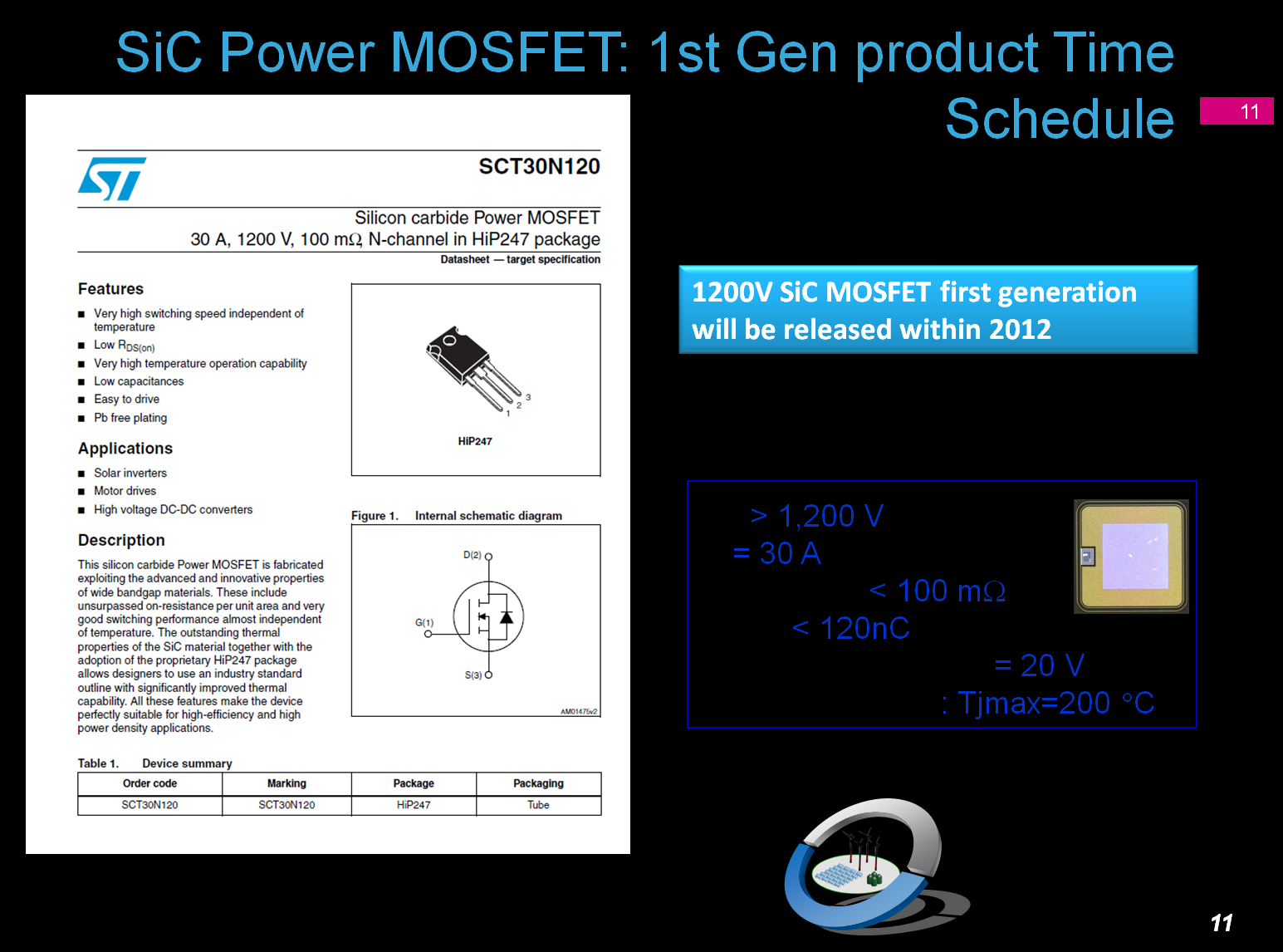
11

12

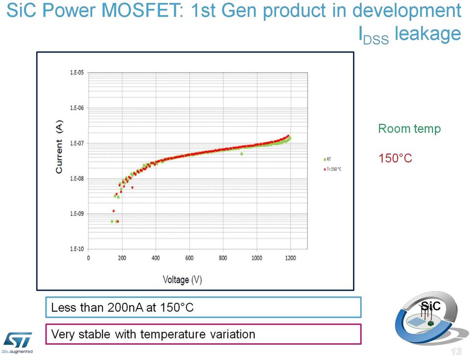
13
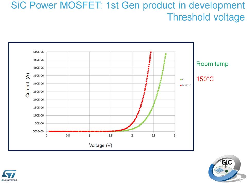
14
15 15 SiC Power MOSFET: 1 st Gen product in development On Resistance vs. Temperature 15 Just 30% higher Ron at 200 C!!

16 SiC MOSFET vs other SiC alternatives Driving needs and switching performances Presentation Title 26/09/2012

17 Different structures in the SiC World 17 The introduction of SiC technology for switching devices rapresents a revolutionary change in the power conversion scenario. Today, three SiC switch technologies (1200V) are offered: SiC JFET SiC BJT SiC MOSFET
 are offered: SiC")
18 Three Different SiC Switches under comparison The target of this work is to compare three different switch tecnologies, both unipolar and bipolar, in terms of driving approach and dynamic losses under the same test conditions. Ron C Ron C NORMALIZED AREA +10% 1200V SiC MOSFET 200 mω (@20V,20A) 220 mω (@20V, 20A) 1 +30% 1200V SiC BJT 90 mω (@6A,130mA) 120 mω (@6A,130mA) % 1200V N-OFF SiC JFET 80 mω (3V,12A) 200 mω (3V,12A) 0.7 We chose to compare three normally-off power switches, due to the higher level of complexity imposed by normally-on devices over the entire system. Direct comparison among different technologies in Silicon Carbide 26/09/2012
 200 mω (3V,12A) 0.")
 and 3V with right current control after turn-on DC current to the gate during conduction is highly dependent on junction temperature.")
19 Driving SiC JFET (1/2) 19 SiC normally off JFET Driving needs Special voltage shape for fast turn-on and correct conduction operation. 15V for a very short time (100/200ns) and 3V with right current control after turn-on DC current to the gate during conduction is highly dependent on junction temperature. At 25 C, 20mA are enough, at 100 C it needs 50mA, and at 125 C up to 200mA. (100mΩ device) Gate threshold is positive but it is too low and decreases increasing Tj. To assure a fast and safe turn-off a negative voltage is mandatory. As suggested in AN SS1 by Semisouth
 Gate threshold is positive but it is too low and decreases increasing Tj.")
20 Driving SiC JFET (2/2) 20 In the following pictures you can observe the V GS =3V vs V GS =15V (limited time) / 3V SJEP120R063 (SemiSouth JFET) Turn Vcc=600V, Ic=12A Vce EON=365µJ -10V +3V 0V Pd=Vce*Ic Vce EON=190µJ Ic Pd=Vce*Ic +15V +3V 0V Ic -10V

21 SiC BJT Driving needs Driving SiC BJT Quite high peak current is requested for a fast BJT turn-on. Higher than the one needed by JFET. Despite the high hfe of last SiC BJT, a constant DC current has to be provided to the base to achieve the right saturation level (means low VCESAT). As for the JFET the BJT prefers a negative driving to minimize turn-off energy and safely keep the OFF state. Device C1 (nf) EON (µj) 80 mω N-OFF JFET 6A V BJT (R oneq = 90mΩ)
22 Driving SiC MOSFET The easiest driving approch 22 Driving a SiC MOSFET is almost as driving a Si MOSFET with a single exception: Vgs to provide to get the right Rdson is higher than the one you need to drive a Si Devices: Today we have to use a 20V Vgs to obtain the lower Rdson. Very simple and very mature gate driver can be used. ST TD350 is an example. Switching speed is higher than the other SiC solutions Negative driving voltage is not mandatory neither to turn-off nor to safely keep the device in OFF state. In fact gate-source threshold voltage is aligned with the one of standard Silicon devices. Negative voltage is suggested only when drain current is high (>50A) to avoid any possible undesired turn-on due to gate voltage oscillations. This is also a commonly used approach with silicon switches used at high current (IGBT)

23 Switching performances: some snapshots SiC MOSFET SiC BJT Turn 600V 23 v gs v ds Qg tot =32.3nC I b I g Eon=28.5 µj I-V cross 20ns v be I d I c v ce Normally off SiC JFET Qg tot =168nC I g v gs +100% Eon=61 µj I-V cross 48ns I d Qg tot =124nC Eon=45.6 µj I-V cross 24ns +50%


24 Switching performances: some snapshots SiC MOSFET SiC BJT Turn 600V 24 v gs v ds v be v ce I g I b I d Qg tot =35.3 nc Eoff 30 µj I c I-V cross 50ns Normally off SiC JFET v gs +100% Qg tot 73nC Eon= 62.7µJ I-V cross 64ns I g Qg tot =49nC Eoff=70.5 µj I-V cross 105ns +130% v ds I d
25 Driving and switching caracteristics summary ON STATE (Id/Ic=5A, 25 C) INPUT VOLTAGE RANGE TURN ON (Ic/Id=5A, Vds/ce=600V, Tj=25 C TURN OFF (Ic/Id=5A, Vds/ce=600V, Tj=25 C TURN OFF VOLTAGE SiC MOSFET Ig[mA] Vgs[V] Vgs th Vgs typ Qgs tot Eon Qgs tot Eoff Vdr 1200V, 200mΩ [V] [nc] [µj] [nc] [µj] [V] SiC BJT Ib[mA] Vbe[V] Vbe min Qbe tot Eon Qbe pk Eoff Vdr 1200V, 80mΩ [V] [nc] [µj] [nc] [µj] [V] n-off SiC JFET 1200V, 90mΩ Ig[mA] Vgs[V] Vgs th Vgs max [V] Qgs tot [nc] Eon [µj] Qgs pk [nc] Eoff [µj] Vdr [V] SiC shows much better dynamic performance still being driven as a standard MOSFET


26 Paper presented at PCIM For further info on how to drive SiC devices please have a look to the above paper
27 Last but not least...what about Freewheeling diode? MOSFET is the only SiC structure to offer intrinsic body diode. Intrinsic Body diode is an ideal diode. It is a SiC diode by nature Freewheeling path in inverters can be one of the following: Through intrinsic diode (High Vf 3V) Through channel by turning MOSFET on and using in the third quadrant Using a SiC JBS external or co-pack freewheeling diode
28 Conclusions 28 Key features Industry Leading Rdson Simple to Drive Body Diode with No Reverse Recovery Charges Very low switching losses with slighty dependance ontemperature Value propositions Smaller Form Factor Lighter Systems Save Size/Cost of Passive Components Higher Systems Efficiency Reduced Cooling Requirements and/or Higher System reliability

29 29 Grazie Thanks 谢 谢
SiC Jfet technology for a jump in Inverter efficiency. SemiSouth Laboratories, Inc. www.semisouth.com
 SiC Jfet technology for a jump in Inverter efficiency SemiSouth Laboratories, Inc. Nigel Springett Applications consultant nigel.springett@semisouth.com www.semisouth.com Italian Distributor Enrico Falloni
Silicon Carbide market update: From discrete devices to modules
 PCIM EUROPE 2014 20th 22nd May 2014 Nuremberg Silicon Carbide market update: From discrete devices to modules Dr. Kamel Madjour, Technology & Market Analyst, Yole Développement 2014 www.yole.fr May 21th
Semiconductor Technology
 May 4 th, 2011 Semiconductor Technology Evolution to optimize inverter efficiency Andrea Merello Field Applications Engineer Page 1 More than 70% of the energy gets lost on its way to the target application
IRLR8743PbF IRLU8743PbF HEXFET Power MOSFET
 Applications l High Frequency Synchronous Buck Converters for Computer Processor Power l High Frequency Isolated DC-DC Converters with Synchronous Rectification for Telecom and Industrial Use l Lead-Free
STGW40NC60V N-CHANNEL 50A - 600V - TO-247 Very Fast PowerMESH IGBT
 N-CHANNEL 50A - 600V - TO-247 Very Fast PowerMESH IGBT Table 1: General Features STGW40NC60V 600 V < 2.5 V 50 A HIGH CURRENT CAPABILITY HIGH FREQUENCY OPERATION UP TO 50 KHz LOSSES INCLUDE DIODE RECOVERY
WFU4N65S Product Description
 65V SuperJunction Power MOSFET Features Ultra low Rdson Ultra low gate charge (typ. Qg =3nC) % UIS tested RoHS compliant G General escription Power MOSFET is fabricated using advanced super junction technology.
Chapter 2. Technical Terms and Characteristics
 Chapter 2 Technical Terms and Characteristics CONTENTS Page 1 IGBT terms 2-2 2 IGBT characteristics 2-5 This section explains relevant technical terms and characteristics of IGBT modules. 2-1 1 IGBT terms
Trench gate field-stop IGBT, M series 650 V, 10 A low loss. Features. Description
 Trench gate field-stop IGBT, M series 650 V, 10 A low loss Datasheet - production data TAB D2PAK 1 3 Features 6 µs of short-circuit withstand time VCE(sat) = 1.55 V (typ.) @ IC = 10 A Tight parameter distribution
UNISONIC TECHNOLOGIES CO., LTD 50N06 Power MOSFET
 UNISONIC TECHNOLOGIES CO., LTD 50N06 50 Amps, 60 Volts N-CHANNEL POWER MOSFET DESCRIPTION TO-263 TO-25 The UTC 50N06 is three-terminal silicon device with current conduction capability of about 50A, fast
TSM2N7002K 60V N-Channel MOSFET
 SOT-23 SOT-323 Pin Definition: 1. Gate 2. Source 3. Drain PRODUCT SUMMARY V DS (V) R DS(on) (Ω) I D (ma) 5 @ V GS = 10V 100 60 5.5 @ V GS = 5V 100 Features Low On-Resistance ESD Protection High Speed Switching
Application Note AN-1070
 Application Note AN-1070 Class D Audio Amplifier Performance Relationship to MOSFET Parameters By Jorge Cerezo, International Rectifier Table of Contents Page Abstract... 2 Introduction... 2 Key MOSFET
N-Channel 60-V (D-S), 175 C MOSFET
, 175 C MOSFET") N-Channel 6-V (D-S), 75 C MOSFET SUP/SUB7N6-4 V (BR)DSS (V) r DS(on) ( ) (A) 6.4 7 a TO-22AB D TO-263 DRAIN connected to TAB G G D S Top View SUP7N6-4 G D S Top View SUB7N6-4 S N-Channel MOSFET Parameter
N-Channel 6-V (D-S), 75 C MOSFET SUP/SUB7N6-4 V (BR)DSS (V) r DS(on) ( ) (A) 6.4 7 a TO-22AB D TO-263 DRAIN connected to TAB G G D S Top View SUP7N6-4 G D S Top View SUB7N6-4 S N-Channel MOSFET Parameter
Final data. Maximum Ratings Parameter Symbol Value Unit
 SPPN8C3 SPN8C3 Cool MOS Power Transistor V DS 8 V Feature R DS(on).45 Ω New revolutionary high voltage technology Ultra low gate charge I D Periodic avalanche rated Extreme dv/dt rated Ultra low effective
N-channel enhancement mode TrenchMOS transistor
 FEATURES SYMBOL QUICK REFERENCE DATA Trench technology d V DSS = V Low on-state resistance Fast switching I D = A High thermal cycling performance Low thermal resistance R DS(ON) mω (V GS = V) g s R DS(ON)
.OPERATING SUPPLY VOLTAGE UP TO 46 V
 L298 DUAL FULL-BRIDGE DRIVER.OPERATING SUPPLY VOLTAGE UP TO 46 V TOTAL DC CURRENT UP TO 4 A. LOW SATURATION VOLTAGE OVERTEMPERATURE PROTECTION LOGICAL "0" INPUT VOLTAGE UP TO 1.5 V (HIGH NOISE IMMUNITY)
Advantages of SiC MOSFETs in Power Applications
 Advantages of SiC MOSFETs in Power Applications Power Forum, Bologna September 18 th, 2014 Pascal Ducluzeau Product Marketing Director Microsemi Power Module Products pducluzeau@microsemi.com Topics Advantages
IRLR8729PbF IRLU8729PbF
 Applications l High Frequency Synchronous Buck Converters for Computer Processor Power l High Frequency Isolated DC-DC Converters with Synchronous Rectification for Telecom and Industrial Use Benefits
IRF150 [REF:MIL-PRF-19500/543] 100V, N-CHANNEL. Absolute Maximum Ratings
![IRF150 [REF:MIL-PRF-19500/543] 100V, N-CHANNEL. Absolute Maximum Ratings](/thumbs/40/21333646.jpg "IRF150 [REF:MIL-PRF-19500/543] 100V, N-CHANNEL. Absolute Maximum Ratings") PD - 90337G REPETITIVE AVALANCHE AND dv/dt RATED HEXFET TRANSISTORS THRU-HOLE (TO-204AA/AE) Product Summary Part Number BVDSS RDS(on) ID IRF150 100V 0.055Ω 38A IRF150 JANTX2N6764 JANTXV2N6764 [REF:MIL-PRF-19500/543]
PD - 90337G REPETITIVE AVALANCHE AND dv/dt RATED HEXFET TRANSISTORS THRU-HOLE (TO-204AA/AE) Product Summary Part Number BVDSS RDS(on) ID IRF150 100V 0.055Ω 38A IRF150 JANTX2N6764 JANTXV2N6764 [REF:MIL-PRF-19500/543]
GS66516T Top-side cooled 650 V E-mode GaN transistor Preliminary Datasheet
 Features 650 V enhancement mode power switch Top-side cooled configuration R DS(on) = 25 mω I DS(max) = 60 A Ultra-low FOM Island Technology die Low inductance GaNPX package Easy gate drive requirements
TOSHIBA Insulated Gate Bipolar Transistor Silicon N Channel IGBT GT60J323
 GT6J2 TOSHIBA Insulated Gate Bipolar Transistor Silicon N Channel IGBT GT6J2 Current Resonance Inverter Switching Application Unit: mm Enhancement mode type High speed : t f =.6 μs (typ.) (I C = 6A) Low
SPW32N50C3. Cool MOS Power Transistor V DS @ T jmax 560 V
 SPW3N5C3 Cool MOS Power Transistor V DS @ T jmax 56 V Feature New revolutionary high voltage technology Ultra low gate charge Periodic avalanche rated Extreme dv/dt rated Ultra low effective capacitances
OptiMOS 3 Power-Transistor
 Type IPD6N3L G OptiMOS 3 Power-Transistor Features Fast switching MOSFET for SMPS Optimized technology for DC/DC converters Qualified according to JEDEC 1) for target applications Product Summary V DS
CoolMOS TM Power Transistor
 CoolMOS TM Power Transistor Features New revolutionary high voltage technology Intrinsic fast-recovery body diode Extremely low reverse recovery charge Ultra low gate charge Extreme dv /dt rated Product
STP80NF55-08 STB80NF55-08 STB80NF55-08-1 N-CHANNEL 55V - 0.0065 Ω - 80A D2PAK/I2PAK/TO-220 STripFET II POWER MOSFET
 STP80NF55-08 STB80NF55-08 STB80NF55-08-1 N-CHANNEL 55V - 0.0065 Ω - 80A D2PAK/I2PAK/TO-220 STripFET II POWER MOSFET TYPE V DSS R DS(on) I D STB80NF55-08/-1 STP80NF55-08 55 V 55 V
STP6NK60Z - STP6NK60ZFP STB6NK60Z - STB6NK60Z-1 N-CHANNEL 600V - 1Ω - 6A TO-220/TO-220FP/D 2 PAK/I 2 PAK Zener-Protected SuperMESH Power MOSFET
 STP6NK60Z - STP6NK60ZFP STB6NK60Z - STB6NK60Z-1 N-CHANNEL 600V - 1Ω - 6A TO-220/TO-220FP/D 2 PAK/I 2 PAK Zener-Protected SuperMESH Power MOSFET TYPE V DSS R DS(on) I D Pw STP6NK60Z STP6NK60ZFP STB6NK60Z
Features. Symbol JEDEC TO-220AB
 Data Sheet June 1999 File Number 2253.2 3A, 5V,.4 Ohm, N-Channel Power MOSFET This is an N-Channel enhancement mode silicon gate power field effect transistor designed for applications such as switching
OptiMOS Power-Transistor Product Summary
 OptiMOS Power-Transistor Product Summary V DS 55 V R DS(on),max 4) 35 mω Features Dual N-channel Logic Level - Enhancement mode AEC Q11 qualified I D 2 A PG-TDSON-8-4 MSL1 up to 26 C peak reflow 175 C
Features. Description. Table 1. Device summary. Order code Marking Package Packing. STP110N8F6 110N8F6 TO-220 Tube
 N-channel 80 V, 0.0056 Ω typ.,110 A, STripFET F6 Power MOSFET in a TO-220 package Features Datasheet - production data Order code V DS R DS(on)max I D P TOT TAB STP110N8F6 80 V 0.0065 Ω 110 A 200 W TO-220
OptiMOS 3 Power-Transistor
 Type IPD36N4L G OptiMOS 3 Power-Transistor Features Fast switching MOSFET for SMPS Optimized technology for DC/DC converters Qualified according to JEDEC ) for target applications Product Summary V DS
V DSS R DS(on) max Qg. 30V 3.2mΩ 36nC
 max Qg. 30V 3.2mΩ 36nC") PD - 96232 Applications l Optimized for UPS/Inverter Applications l High Frequency Synchronous Buck Converters for Computer Processor Power l High Frequency Isolated DC-DC Converters with Synchronous Rectification
PD - 96232 Applications l Optimized for UPS/Inverter Applications l High Frequency Synchronous Buck Converters for Computer Processor Power l High Frequency Isolated DC-DC Converters with Synchronous Rectification
AUTOMOTIVE MOSFET. C Soldering Temperature, for 10 seconds 300 (1.6mm from case )
") PD 9399A AUTOMOTIVE MOSFET Typical Applications Electric Power Steering (EPS) Antilock Braking System (ABS) Wiper Control Climate Control Power Door Benefits Advanced Process Technology Ultra Low OnResistance
PD 9399A AUTOMOTIVE MOSFET Typical Applications Electric Power Steering (EPS) Antilock Braking System (ABS) Wiper Control Climate Control Power Door Benefits Advanced Process Technology Ultra Low OnResistance
BUZ11. 30A, 50V, 0.040 Ohm, N-Channel Power MOSFET. Features. [ /Title (BUZ1 1) /Subject. (30A, 50V, 0.040 Ohm, N- Channel. Ordering Information
 /Subject. (30A, 50V, 0.040 Ohm, N- Channel. Ordering Information") Data Sheet June 1999 File Number 2253.2 [ /Title (BUZ1 1) /Subject (3A, 5V,.4 Ohm, N- Channel Power MOS- FET) /Autho r () /Keywords (Intersil Corporation, N- Channel Power MOS- FET, TO- 22AB ) /Creator
Data Sheet June 1999 File Number 2253.2 [ /Title (BUZ1 1) /Subject (3A, 5V,.4 Ohm, N- Channel Power MOS- FET) /Autho r () /Keywords (Intersil Corporation, N- Channel Power MOS- FET, TO- 22AB ) /Creator
N-Channel 20-V (D-S) 175 C MOSFET
 175 C MOSFET") N-Channel -V (D-S) 75 C MOSFET SUD7N-4P PRODUCT SUMMARY V DS (V) r DS(on) ( ) (A) a.37 @ V GS = V 37.6 @ V GS = 4.5 V 9 TO-5 D FEATURES TrenchFET Power MOSFET 75 C Junction Temperature PWM Optimized for
N-Channel -V (D-S) 75 C MOSFET SUD7N-4P PRODUCT SUMMARY V DS (V) r DS(on) ( ) (A) a.37 @ V GS = V 37.6 @ V GS = 4.5 V 9 TO-5 D FEATURES TrenchFET Power MOSFET 75 C Junction Temperature PWM Optimized for
STB4NK60Z, STB4NK60Z-1, STD4NK60Z STD4NK60Z-1, STP4NK60Z,STP4NK60ZFP
 STB4NK60Z, STB4NK60Z-1, STD4NK60Z STD4NK60Z-1, STP4NK60Z,STP4NK60ZFP N-channel 600 V - 1.76 Ω - 4 A SuperMESH Power MOSFET DPAK - D 2 PAK - IPAK - I 2 PAK - TO-220 - TO-220FP Features Type V DSS R DS(on)
STP10NK60Z/FP, STB10NK60Z/-1 STW10NK60Z N-CHANNEL 600V-0.65Ω-10A TO-220/FP/D 2 PAK/I 2 PAK/TO-247 Zener-Protected SuperMESH Power MOSFET
 STP10NK60Z/FP, STB10NK60Z/-1 STW10NK60Z N-CHANNEL 600V-0.65Ω-10A TO-220/FP/D 2 PAK/I 2 PAK/TO-247 Zener-Protected SuperMESH Power MOSFET TYPE V DSS R DS(on) I D Pw STP10NK60Z STP10NK60ZFP STB10NK60Z STB10NK60Z-1
1ED Compact A new high performance, cost efficient, high voltage gate driver IC family
 1ED Compact A new high performance, cost efficient, high voltage gate driver IC family Heiko Rettinger, Infineon Technologies AG, Am Campeon 1-12, 85579 Neubiberg, Germany, heiko.rettinger@infineon.com
Features Benefits Applications
 N9 N-Channel JFET Product Summary V GS(off) (V) V (BR)GSS Min (V) g fs Min SS Min (ma) 5 Features Benefits Applications Excellent High-Frequency Gain: Gps db @ MHz Very Low Noise: db @ MHz Very Low Distortion
N-Channel 60-V (D-S) MOSFET
 MOSFET") 7/7, VQJ/P, BS7 -Channel 6-V (D-S) MOSFET Part umber V (BR)DSS Min (V) r DS(on) Max ( ) V GS(th) (V) I D (A) 7 5 @ V GS = V.8 to. 7 7.5 @ V GS = V to.5.5 VQJ 6 5.5 @ V GS = V.8 to.5.5 VQP 5.5 @ V GS =
7/7, VQJ/P, BS7 -Channel 6-V (D-S) MOSFET Part umber V (BR)DSS Min (V) r DS(on) Max ( ) V GS(th) (V) I D (A) 7 5 @ V GS = V.8 to. 7 7.5 @ V GS = V to.5.5 VQJ 6 5.5 @ V GS = V.8 to.5.5 VQP 5.5 @ V GS =
Features. T A=25 o C unless otherwise noted. Symbol Parameter Ratings Units. (Note 1b) 0.46
 0.46") N-Channel.8 Vgs Specified PowerTrench MOSFET October 2 General Description This 2V N-Channel MOSFET uses Fairchild s high voltage PowerTrench process. It has been optimized for power management applications.
N-Channel.8 Vgs Specified PowerTrench MOSFET October 2 General Description This 2V N-Channel MOSFET uses Fairchild s high voltage PowerTrench process. It has been optimized for power management applications.
Quad, Rail-to-Rail, Fault-Protected, SPST Analog Switches
 19-2418; Rev ; 4/2 Quad, Rail-to-Rail, Fault-Protected, General Description The are quad, single-pole/single-throw (SPST), fault-protected analog switches. They are pin compatible with the industry-standard
IRF830. N - CHANNEL 500V - 1.35Ω - 4.5A - TO-220 PowerMESH MOSFET
 IRF830 N - CHANNEL 500V - 1.35Ω - 4.5A - TO-220 PowerMESH MOSFET TYPE V DSS R DS(on) I D IRF830 500 V < 1.5 Ω 4.5 A TYPICAL R DS(on) = 1.35 Ω EXTREMELY HIGH dv/dt CAPABILITY 100% AVALANCHE TESTED VERY
5SNA 3600E170300 HiPak IGBT Module
 Data Sheet, Doc. No. 5SYA 44-6 2-24 5SNA 36E73 HiPak IGBT Module VCE = 7 V IC = 36 A Ultra low-loss, rugged SPT+ chip-set Smooth switching SPT+ chip-set for good EMC AlSiC base-plate for high power cycling
OptiMOS TM Power-Transistor
 Type BSC28N6NS OptiMOS TM Power-Transistor Features Optimized for high performance SMPS, e.g. sync. rec. % avalanche tested Superior thermal resistance N-channel Qualified according to JEDEC ) for target
IRF6201PbF. HEXFET Power MOSFET V DS 20 V. R DS(on) max. 2.75 mω. Q g (typical) 130 nc 27 A. Absolute Maximum Ratings
 max. 2.75 mω. Q g (typical) 130 nc 27 A. Absolute Maximum Ratings") PD - 97500A IRF620PbF V DS 20 V HEXFET Power MOSFET R DS(on) max (@ = 4.5V) 2.45 mω 6 R DS(on) max (@ = 2.5V) 2.75 mω 6 6 Q g (typical) 30 nc * SO-8 I D (@T A = 25 C) 27 A Applications OR-ing or hot-swap
PD - 97500A IRF620PbF V DS 20 V HEXFET Power MOSFET R DS(on) max (@ = 4.5V) 2.45 mω 6 R DS(on) max (@ = 2.5V) 2.75 mω 6 6 Q g (typical) 30 nc * SO-8 I D (@T A = 25 C) 27 A Applications OR-ing or hot-swap
Features. P-Channel Enhancement Mode MOSFET
 P-Channel Enhancement Mode MOSFET Features Pin Description -4V/-25, R DS(ON) = 4mΩ (typ.) @ V GS = -V R DS(ON) = 55mΩ (typ.) @ V GS = -5V Super High Dense Cell Design G D S Reliable and Rugged Lead Free
SD4840/4841/4842/4843/4844
 CURRENT MODE PWM CONTROLLER WITH BUILT-IN HIGH VOLTAGE MOSFET DESCRIPTION SD4840/4841/4842/4843/4844 is a current mode PWM controller with low standby power and low start current for power switch. In standby
STP10NK80ZFP STP10NK80Z - STW10NK80Z
 STP10NK80ZFP STP10NK80Z - STW10NK80Z N-channel 800V - 0.78Ω - 9A - TO-220/FP-TO-247 Zener-protected supermesh TM MOSFET General features Type V DSS R DS(on) I D Pw STP10NK80Z 800V
STW20NM50 N-CHANNEL 550V @ Tjmax - 0.20Ω - 20ATO-247 MDmesh MOSFET
 N-CHANNEL 550V @ Tjmax - 0.20Ω - 20ATO-247 MDmesh MOSFET TYPE V DSS (@Tjmax) R DS(on) I D STW20NM50 550V < 0.25Ω 20 A TYPICAL R DS (on) = 0.20Ω HIGH dv/dt AND AVALANCHE CAPABILITIES 100% AVALANCHE TESTED
C Soldering Temperature, for 10 seconds 300 (1.6mm from case )
") l Advanced Process Technology l Ultra Low On-Resistance l Dynamic dv/dt Rating l 75 C Operating Temperature l Fast Switching l Fully Avalanche Rated l Optimized for SMPS Applications Description Advanced
l Advanced Process Technology l Ultra Low On-Resistance l Dynamic dv/dt Rating l 75 C Operating Temperature l Fast Switching l Fully Avalanche Rated l Optimized for SMPS Applications Description Advanced
IGBT vs. MOSFET : Which Device to Select?
 IGBT vs. MOSFET : Which Device to Select? Renesas Electronics America Inc. Renesas Technology & Solution Portfolio 2 Enabling The Smart Society Challenge: The challenge of the smart society is to create
AN-6005 Synchronous buck MOSFET loss calculations with Excel model
 www.fairchildsemi.com Synchronous buck MOSFET loss calculations with Excel model Jon Klein Power Management Applications Abstract The synchronous buck circuit is in widespread use to provide point of use
RoHS Compliant Containing no Lead, no Bromide and no Halogen. IRF9310PbF SO8 Tube/Bulk 95 IRF9310TRPbF SO8 Tape and Reel 4000
 PD 97437A IRF93PbF HEXFET Power MOSFET V DS 30 V R DS(on) max (@V GS = V) I D (@T A = 25 C) 4. mω 20 A * SO8 Applications Charge and Discharge Switch for Notebook PC Battery Application Features and Benefits
FDD4243 40V P-Channel PowerTrench MOSFET -40V, -14A, 44mΩ Features
 FDD443 4V P-Channel PowerTrench MOSFET -4V, -4A, 44mΩ Features Max r DS(on) = 44mΩ at V GS = -V, I D = -6.7A Max r DS(on) = 64mΩ at V GS = -4.5V, I D = -5.5A High performance trench technology for extremely
Symbol Parameter Value Unit V DS Drain-source Voltage (V GS =0) 50 V V DGR Drain- gate Voltage (R GS =20kΩ) 50 V
 50 V V DGR Drain- gate Voltage (R GS =20kΩ) 50 V") BUZ71A N - CHANNEL 50V - 0.1Ω - 13A TO-220 STripFET POWER MOSFET TYPE V DSS R DS(on) I D BUZ71A 50 V < 0.12 Ω 13 A TYPICAL RDS(on) = 0.1 Ω AVALANCHE RUGGED TECHNOLOGY 100% AVALANCHE TESTED HIGH CURRENT
BUZ71A N - CHANNEL 50V - 0.1Ω - 13A TO-220 STripFET POWER MOSFET TYPE V DSS R DS(on) I D BUZ71A 50 V < 0.12 Ω 13 A TYPICAL RDS(on) = 0.1 Ω AVALANCHE RUGGED TECHNOLOGY 100% AVALANCHE TESTED HIGH CURRENT
IRGP4068DPbF IRGP4068D-EPbF
 INSULATED GATE BIPOLAR TRANSISTOR WITH ULTRA-LOW VF DIODE FOR INDUCTION HEATING AND SOFT SWITCHING APPLICATIONS Features Low V CE (ON) Trench IGBT Technology Low Switching Losses Maximum Junction temperature
IRFP450. N - CHANNEL 500V - 0.33Ω - 14A - TO-247 PowerMESH MOSFET
 IRFP450 N - CHANNEL 500V - 0.33Ω - 14A - TO-247 PowerMESH MOSFET TYPE V DSS R DS(on) I D IRFP450 500 V < 0.4 Ω 14 A TYPICAL R DS(on) = 0.33 Ω EXTREMELY HIGH dv/dt CAPABILITY 100% AVALANCHE TESTED VERY
TPN4R712MD TPN4R712MD. 1. Applications. 2. Features. 3. Packaging and Internal Circuit. 2014-12 2015-04-21 Rev.4.0. Silicon P-Channel MOS (U-MOS )
") MOSFETs Silicon P-Channel MOS (U-MOS) TPN4R712MD TPN4R712MD 1. Applications Lithium-Ion Secondary Batteries Power Management Switches 2. Features (1) Low drain-source on-resistance: R DS(ON) = 3.8 mω (typ.)
MOSFETs Silicon P-Channel MOS (U-MOS) TPN4R712MD TPN4R712MD 1. Applications Lithium-Ion Secondary Batteries Power Management Switches 2. Features (1) Low drain-source on-resistance: R DS(ON) = 3.8 mω (typ.)
P-Channel 1.25-W, 1.8-V (G-S) MOSFET
 MOSFET") Si5DS P-Channel.5-W,.-V (G-S) MOSFET PRODUCT SUMMARY V DS (V) R DS(on) (Ω) I D (A).5 at V GS = -.5 V ±.5 -.7 at V GS = -.5 V ±. at V GS = -. V ± FEATURES Halogen-free According to IEC 9-- Available TrenchFET
Si5DS P-Channel.5-W,.-V (G-S) MOSFET PRODUCT SUMMARY V DS (V) R DS(on) (Ω) I D (A).5 at V GS = -.5 V ±.5 -.7 at V GS = -.5 V ±. at V GS = -. V ± FEATURES Halogen-free According to IEC 9-- Available TrenchFET
STP6N60FI N - CHANNEL ENHANCEMENT MODE POWER MOS TRANSISTOR
 N - CHANNEL ENHANCEMENT MODE POWER MOS TRANSISTOR TYPE VDSS RDS(on) ID STP6N60FI 600 V < 1.2 Ω 3.8 A TYPICAL R DS(on) =1Ω AVALANCHE RUGGED TECHNOLOGY 100% AVALANCHE TESTED REPETITIVE AVALANCHE DATA AT
Transistor MOS. Ce Dossier comporte 10 pages comme suit : - Page 1 : Fonctionnement du transistor MOS
 Transistor MOS Ce Dossier comporte 10 pages comme suit : - Page 1 : Fonctionnement du transistor MOS - Pages 2 à 9 : Documentation constructeur VNP49N04 NOTA : Tous les documents fournis seront remis à
30 V, single N-channel Trench MOSFET
 SOT883B Rev. 1 11 May 212 Product data sheet 1. Product profile 1.1 General description N-channel enhancement mode Field-Effect Transistor (FET) in a leadless ultra small DFN16B-3 (SOT883B) Surface-Mounted
N-channel TrenchMOS logic level FET
 SOT23 Rev. 2 7 November 2 Product data sheet. Product profile. General description Logic level N-channel enhancement mode Field-Effect Transistor (FET) in a plastic package using TrenchMOS technology.
Peak Atlas DCA. Semiconductor Component Analyser Model DCA55. User Guide
 GB55-7 Peak Atlas DCA Semiconductor Component Analyser Model DCA55 User Guide Peak Electronic Design Limited 2000/2007 In the interests of development, information in this guide is subject to change without
SIPMOS Small-Signal-Transistor
 SIPMOS Small-Signal-Transistor Features N-channel Depletion mode dv /dt rated Product Summary V DS V R DS(on),max 3.5 Ω I DSS,min.4 A Available with V GS(th) indicator on reel Pb-free lead plating; RoHS
Lower Conduction Losses Low Thermal Resistance to PCB ( 0.5 C/W)
") PD -97428 IRFH5020PbF HEXFET Power MOSFET V DS 200 V 55 m: R DS(on) max (@V GS = V) Q g (typical) 36 nc R G (typical).9 : I D (@T c(bottom) = 25 C) 43 A PQFN 5X6 mm Applications Secondary Side Synchronous
PD -97428 IRFH5020PbF HEXFET Power MOSFET V DS 200 V 55 m: R DS(on) max (@V GS = V) Q g (typical) 36 nc R G (typical).9 : I D (@T c(bottom) = 25 C) 43 A PQFN 5X6 mm Applications Secondary Side Synchronous
RFG70N06, RFP70N06, RF1S70N06, RF1S70N06SM
 A M A A December 995 SEMICONDUCTOR RFG7N6, RFP7N6, RFS7N6, RFS7N6SM 7A, 6V, Avalanche Rated, N-Channel Enhancement-Mode Power MOSFETs Features 7A, 6V r DS(on) =.4Ω Temperature Compensated PSPICE Model
STN3NF06L. N-channel 60 V, 0.07 Ω, 4 A, SOT-223 STripFET II Power MOSFET. Features. Application. Description
 N-channel 60 V, 0.07 Ω, 4 A, SOT-223 STripFET II Power MOSFET Features Type V DSS (@Tjmax) Exceptional dv/dt capability Avalanche rugged technology 100% avalanche tested R DS(on) max STN3NF06L 60 V < 0.1
IRF740 N-CHANNEL 400V - 0.46Ω - 10A TO-220 PowerMESH II MOSFET
 N-CHANNEL 400V - 0.46Ω - 10A TO-220 PowerMESH II MOSFET TYPE V DSS R DS(on) I D IRF740 400 V < 0.55 Ω 10 A TYPICAL R DS (on) = 0.46Ω EXCEPTIONAL dv/dt CAPABILITY 100% AVALANCHE TESTED LOW GATE CHARGE VERY
AN ISOLATED GATE DRIVE FOR POWER MOSFETs AND IGBTs
 APPLICATION NOTE AN ISOLATED GATE DRIVE FOR POWER MOSFETs AND IGBTs by J.M. Bourgeois ABSTRACT Power MOSFET and IGBT gate drives often face isolation and high voltage constraints. The gate drive described
SMPS MOSFET. V DSS Rds(on) max I D
 max I D") Applications l Switch Mode Power Supply ( SMPS ) l Uninterruptable Power Supply l High speed power switching SMPS MOSFET PD 92004 IRF740A HEXFET Power MOSFET V DSS Rds(on) max I D 400V 0.55Ω A Benefits
Applications l Switch Mode Power Supply ( SMPS ) l Uninterruptable Power Supply l High speed power switching SMPS MOSFET PD 92004 IRF740A HEXFET Power MOSFET V DSS Rds(on) max I D 400V 0.55Ω A Benefits
Symbol Parameter Value Unit IAR Avalanche Current, Repetitive or Not-Repetitive
 BUZ11 N - CHANNEL 50V - 0.03Ω - 30A -TO-220 STripFET POWER MOSFET TYPE V DSS R DS(on) I D BUZ11 50 V < 0.04 Ω 30 A TYPICAL R DS(on) = 0.03 Ω AVALANCHE RUGGED TECHNOLOGY 100% AVALANCHE TESTED HIGH CURRENT
Power MOSFET Tutorial
 Power MOSFET Tutorial Jonathan Dodge, P.E. Applications Engineering Manager Advanced Power Technology 405 S.W. Columbia Street Bend, OR 97702 Introduction Power MOSFETs are well known for superior switching
How To Make A Field Effect Transistor (Field Effect Transistor) From Silicon P Channel (Mos) To P Channel Power (Mos) (M2) (Mm2)
 From Silicon P Channel (Mos) To P Channel Power (Mos) (M2) (Mm2)") TPC811 TOSHIBA Field Effect Transistor Silicon P Channel MOS Type (U-MOS III) TPC811 Lithium Ion Battery Applications Notebook PC Applications Portable Equipment Applications Unit: mm Small footprint due
TPC811 TOSHIBA Field Effect Transistor Silicon P Channel MOS Type (U-MOS III) TPC811 Lithium Ion Battery Applications Notebook PC Applications Portable Equipment Applications Unit: mm Small footprint due
VNP5N07 "OMNIFET": FULLY AUTOPROTECTED POWER MOSFET
 "OMNIFET": FULLY AUTOPROTECTED POWER MOSFET TYPE Vclamp RDS(on) Ilim VNP5N07 70 V 0.2 Ω 5 A LINEAR CURRENT LIMITATION THERMAL SHUT DOWN SHORT CIRCUIT PROTECTION INTEGRATED CLAMP LOW CURRENT DRAWN FROM
High Voltage Silicon Carbide Power Devices
 High Voltage Silicon Carbide Power Devices ARPA-E Power Technologies Workshop February 9, 2010 John W. Palmour Cree, Inc. 4600 Silicon Drive Durham, NC 27703; USA Tel:: 919-313-5646 Email: john_palmour@cree.com
Zero voltage drop synthetic rectifier
 Zero voltage drop synthetic rectifier Vratislav Michal Brno University of Technology, Dpt of Theoretical and Experimental Electrical Engineering Kolejní 4/2904, 612 00 Brno Czech Republic vratislav.michal@gmail.com,
200V, N-CHANNEL. Absolute Maximum Ratings. Features: www.irf.com 1 PD - 90370
 PD - 90370 REPETITIVE AVALANCHE AND dv/dt RATED HEXFET TRANSISTORS THRU-HOLE (TO-204AA/AE) IRF240 200V, N-CHANNEL Product Summary Part Number BVDSS RDS(on) ID IRF240 200V 0.18Ω 18A The HEXFET technology
A new SOI Single Chip Inverter IC implemented into a newly designed SMD package
 A new SOI Single Chip Inverter IC implemented into a newly designed SMD package Kiyoto Watabe**, Marco Honsberg*, Hatade Kazunari** and Toru Araki** **Mitsubishi Electric Corp., Power Device Works, 1-1-1,
W/ C V GS Gate-to-Source Voltage ± 20 dv/dt Peak Diode Recovery e 38. V/ns T J. mj I AR
 PD 967 IRFB465PbF Applications l High Efficiency Synchronous Rectification in SMPS l Uninterruptible Power Supply l High Speed Power Switching l Hard Switched and High Frequency Circuits G D S V DSS HEXFET
Power MOSFET. IRF510PbF SiHF510-E3 IRF510 SiHF510. PARAMETER SYMBOL LIMIT UNIT Drain-Source Voltage V DS 100 V Gate-Source Voltage V GS ± 20
 Power MOSFET PRODUCT SUMMARY (V) 100 R DS(on) () = 0.54 Q g max. (nc) 8.3 Q gs (nc) 2.3 Q gd (nc) 3.8 Configuration Single D TO220AB G FEATURES Dynamic dv/dt rating Available Repetitive avalanche rated
91 P D @T C = 25 C Power Dissipation 330 P D @T C = 100 C Power Dissipation Linear Derating Factor
 PD - 9778 IRFB4229PbF Features l dvanced Process Technology l Key Parameters Optimized for PDP Sustain, Energy Recovery and Pass Switch pplications l Low E PULSE Rating to Reduce Power Dissipation in PDP
Power MOSFET FEATURES. IRFZ44PbF SiHFZ44-E3 IRFZ44 SiHFZ44 T C = 25 C
 Power MOSFET PRODUCT SUMMARY (V) 60 R DS(on) (Ω) V GS = 10 V 0.028 Q g (Max.) (nc) 67 Q gs (nc) 18 Q gd (nc) 25 Configuration Single FEATURES Dynamic dv/dt Rating 175 C Operating Temperature Fast Switching
W/ C V GS Gate-to-Source Voltage ± 16 dv/dt Peak Diode Recovery e 21
 PD 97369 IRLB43PbF Applications l DC Motor Drive l High Efficiency Synchronous Rectification in SMPS l Uninterruptible Power Supply l High Speed Power Switching l Hard Switched and High Frequency Circuits
Power MOSFET FEATURES. IRL540PbF SiHL540-E3 IRL540 SiHL540
 Power MOSFET PRODUCT SUMMARY (V) 100 R DS(on) (Ω) = 5.0 V 0.077 Q g (Max.) (nc) 64 Q gs (nc) 9.4 Q gd (nc) 27 Configuration Single TO220AB G DS ORDERING INFORMATION Package Lead (Pb)free SnPb G D S NChannel
P-Channel 20 V (D-S) MOSFET
 MOSFET") Si30CDS P-Channel 0 V (D-S) MOSFET MOSFET PRODUCT SUMMARY V DS (V) R DS(on) ( ) I D (A) a Q g (Typ.) - 0 0. at V GS = - 4.5 V - 3. 0.4 at V GS = -.5 V -.7 3.3 nc TO-36 (SOT-3) FEATURES Halogen-free According
Si30CDS P-Channel 0 V (D-S) MOSFET MOSFET PRODUCT SUMMARY V DS (V) R DS(on) ( ) I D (A) a Q g (Typ.) - 0 0. at V GS = - 4.5 V - 3. 0.4 at V GS = -.5 V -.7 3.3 nc TO-36 (SOT-3) FEATURES Halogen-free According
Power MOSFET FEATURES. IRF610PbF SiHF610-E3 IRF610 SiHF610. PARAMETER SYMBOL LIMIT UNIT Drain-Source Voltage V DS 200 V Gate-Source Voltage V GS ± 20
 Power MOSFET PRODUCT SUMMARY (V) 00 R DS(on) ( ) = 1.5 Q g (Max.) (nc) 8. Q gs (nc) 1.8 Q gd (nc) 4.5 Configuration Single FEATURES Dynamic dv/dt Rating Repetitive Avalanche Rated Fast Switching Ease of
N-Channel 40-V (D-S) 175 C MOSFET
 175 C MOSFET") N-Channel 4-V (D-S) 75 C MOSFET SUP/SUB85N4-4 PRODUCT SUMMARY V (BR)DSS (V) r DS(on) ( ) (A) 4.4 @ V GS = V 85 a TO-22AB D TO-263 G DRAIN connected to TAB G D S Top View Ordering Information SUP85N4-4
N-Channel 4-V (D-S) 75 C MOSFET SUP/SUB85N4-4 PRODUCT SUMMARY V (BR)DSS (V) r DS(on) ( ) (A) 4.4 @ V GS = V 85 a TO-22AB D TO-263 G DRAIN connected to TAB G D S Top View Ordering Information SUP85N4-4
2SD315AI Dual SCALE Driver Core for IGBTs and Power MOSFETs
 2SD315AI Dual SCALE Driver Core for IGBTs and Power MOSFETs Description The SCALE drivers from CONCEPT are based on a chip set that was developed specifically for the reliable driving and safe operation
Power MOSFET FEATURES. IRF740PbF SiHF740-E3 IRF740 SiHF740. PARAMETER SYMBOL LIMIT UNIT Drain-Source Voltage V DS 400 V Gate-Source Voltage V GS ± 20
 Power MOSFET PRODUCT SUMMARY (V) 400 R DS(on) (Ω) = 0.55 Q g (Max.) (nc) 63 Q gs (nc) 9.0 Q gd (nc) 3 Configuration Single FEATURES Dynamic dv/dt Rating Repetitive Avalanche Rated Fast Switching Ease of
STB60N55F3, STD60N55F3, STF60N55F3 STI60N55F3, STP60N55F3, STU60N55F3
 STB60N55F3, STD60N55F3, STF60N55F3 STI60N55F3, STP60N55F3, STU60N55F3 N-channel 55 V, 6.5 mω, 80 A, DPAK, IPAK, D 2 PAK, I 2 PAK, TO-220 TO-220FP STripFET III Power MOSFET Features Type V DSS R DS(on)
= 600 V = 56 A = 2.7 V. C2-Class High Speed IGBTs (Electrically Isolated Back Surface) = 32 ns V CE(SAT) t fi(typ. Preliminary Data Sheet
 = 32 ns V CE(SAT) t fi(typ. Preliminary Data Sheet") HiPerFAST TM IGBT IXGR 4N6C2 ISOPLUS247 TM IXGR 4N6C2D C2-Class High Speed IGBTs (Electrically Isolated Back Surface) S = 6 V 25 = 56 A (SAT) = 2.7 V t fi(typ = 32 ns Preliminary Data Sheet IXGR_C2 IXGR_C2D
HiPerFAST TM IGBT IXGR 4N6C2 ISOPLUS247 TM IXGR 4N6C2D C2-Class High Speed IGBTs (Electrically Isolated Back Surface) S = 6 V 25 = 56 A (SAT) = 2.7 V t fi(typ = 32 ns Preliminary Data Sheet IXGR_C2 IXGR_C2D
C Soldering Temperature, for 10 seconds 300 (1.6mm from case )
") dvanced Process Technology Dynamic dv/dt Rating 75 C Operating Temperature Fast Switching Fully valanche Rated Lead-Free Description Fifth Generation HEXFETs from International Rectifier utilize advanced
dvanced Process Technology Dynamic dv/dt Rating 75 C Operating Temperature Fast Switching Fully valanche Rated Lead-Free Description Fifth Generation HEXFETs from International Rectifier utilize advanced
IRF5305PbF. HEXFET Power MOSFET V DSS = -55V. R DS(on) = 0.06Ω I D = -31A
 = 0.06Ω I D = -31A") dvanced Process Technology Dynamic dv/dt Rating 75 C Operating Temperature Fast Switching PChannel Fully valanche Rated LeadFree Description Fifth Generation HEXFETs from International Rectifier utilize
dvanced Process Technology Dynamic dv/dt Rating 75 C Operating Temperature Fast Switching PChannel Fully valanche Rated LeadFree Description Fifth Generation HEXFETs from International Rectifier utilize
Eliminating Parasitic Oscillation between Parallel MOSFETs
 Eliminating Parasitic Oscillation between Parallel MOSFETs Based in part on a paper presented at Power Electronics Technology 2003 conference titled Issues with Paralleling MOSFETs and IGBTs by Jonathan
IRFR3707Z IRFU3707Z HEXFET Power MOSFET
 Applications l High Frequency Synchronous Buck Converters for Computer Processor Power l High Frequency Isolated DC-DC Converters with Synchronous Rectification for Telecom and Industrial Use Benefits
P-Channel 20-V (D-S) MOSFET
 MOSFET") Si33DS P-Channel -V (D-S) MOSFET PRODUCT SUMMARY V DS (V) R DS(on) (Ω) I D (A).39 at V GS = -.5 V -.7 -.5 at V GS = -.5 V -..68 at V GS = -.8 V - 3.5 FEATURES Halogen-free According to IEC 69-- Available
Si33DS P-Channel -V (D-S) MOSFET PRODUCT SUMMARY V DS (V) R DS(on) (Ω) I D (A).39 at V GS = -.5 V -.7 -.5 at V GS = -.5 V -..68 at V GS = -.8 V - 3.5 FEATURES Halogen-free According to IEC 69-- Available
OBJECTIVE QUESTIONS IN ANALOG ELECTRONICS
 1. The early effect in a bipolar junction transistor is caused by (a) fast turn-on (c) large collector-base reverse bias (b)fast turn-off (d) large emitter-base forward bias 2. MOSFET can be used as a
Features 1.7 A, 20 V. R DS(ON) Symbol Parameter Ratings Units
 Symbol Parameter Ratings Units") N-Channel.5V Specified PowerTrench TM MOSFET April 999 General Description This N-Channel.5V specified MOSFET is produced using Fairchild Semiconductor's advanced PowerTrench process that has been especially
N-Channel.5V Specified PowerTrench TM MOSFET April 999 General Description This N-Channel.5V specified MOSFET is produced using Fairchild Semiconductor's advanced PowerTrench process that has been especially
TSM020N03PQ56 30V N-Channel MOSFET
 PDFN56 Pin Definition: 1. Source 8. Drain 2. Source 7. Drain 3. Source 6. Drain 4. Gate 5. Drain Key Parameter Performance Parameter Value Unit V DS 30 V R DS(on) (max) V GS = 10V 2 V GS = 4.5V 3 mω Q
V DSS I D. W/ C V GS Gate-to-Source Voltage ±30 E AS (Thermally limited) mj T J Operating Junction and -55 to + 175
 mj T J Operating Junction and -55 to + 175") PD 973B IRFB432PbF Applications l Motion Control Applications l High Efficiency Synchronous Rectification in SMPS l Uninterruptible Power Supply l Hard Switched and High Frequency Circuits Benefits l Low
PD 973B IRFB432PbF Applications l Motion Control Applications l High Efficiency Synchronous Rectification in SMPS l Uninterruptible Power Supply l Hard Switched and High Frequency Circuits Benefits l Low