FSDH0265RN, FSDM0265RN
|
|
|
- Lawrence Gray
- 10 years ago
- Views:
Transcription
1 Green Mode Fairchild Power Switch (FPS TM ) Features Internal Avalanche Rugged Sense FET Consumes only 0.65W at 240VAC & 0.3W load with Advanced Burst-Mode Operation Frequency Modulation for EMI Reduction Precision Fixed Operating Frequency Internal Start-up Circuit Pulse-by-Pulse Current Limiting Abnormal Over Current Protection (AOCP) Over Voltage Protection (OVP) Over Load Protection (OLP) Internal Thermal Shutdown Function (TSD) Auto-Restart Mode Under Voltage Lockout (UVLO) Low Operating Current (3mA) Adjustable Peak Current Limit Built-in Soft Start Applications SMPS for VCR, SVR, STB, DVD & DVCD Player SMPS for Printer, Facsimile & Scanner Adapter for Camcorder Related Application Notes AN-4137, 4141, 4147(Flyback) / AN-4134(Forward) Description Each product in the FSDx0265RN (x for M, H) family consists of an integrated Pulse Width Modulator (PWM) and Sense FET, and is specifically designed for high performance off-line Switch Mode Power Supplies (SMPS) with minimal external components. Both devices are integrated high voltage power switching regulators which combine an avalanche rugged Sense FET with a current mode PWM control block. The integrated PWM controller features include: a fixed oscillator with frequency modulation for reduced EMI, Under Voltage Lock Out (UVLO) protection, Leading Edge Blanking (LEB), an optimized gate turn-on/ turn-off driver, Thermal Shut Down (TSD) protection, Abnormal Over Current Protection (AOCP) and temperature compensated precision current sources for loop compensation and fault protection circuitry. When compared to a discrete MOSFET and controller or RCC switching converter solution, the FSDx0265RN devices reduce total component count, design size, weight while increasing efficiency, productivity and system reliability. Both devices provide a basic platform that is well suited for the design of cost-effective flyback converters. FPS TM is a trademark of Fairchild Semiconductor Corporation. OUTPUT POWER TABLE 230VAC ±15% (3) VAC PRODUCT Adapter Open Frame (2) Adapter Open Frame (2) FSDL321 11W 17W 8W 12W FSDH321 11W 17W 8W 12W FSDL0165RN 13W 23W 11W 17W FSDM0265RN 16W 27W 13W 20W FSDH0265RN 16W 27W 13W 20W FSDL0365RN 19W 30W 16W 24W FSDM0365RN 19W 30W 16W 24W FSDL321L 11W 17W 8W 12W FSDH321L 11W 17W 8W 12W FSDL0165RL 13W 23W 11W 17W FSDM0265RL 16W 27W 13W 20W FSDH0265RL 16W 27W 13W 20W FSDL0365RL 19W 30W 16W 24W FSDM0365RL 19W 30W 16W 24W Notes: 1. Typical continuous power in a non-ventilated enclosed adapter with sufficient drain pattern as a heat sinker, at 50 C ambient. 2. Maximum practical continuous power in an open frame design with sufficient drain pattern as a heat sinker, at 50 C ambient VAC or 100/115 VAC with doubler. Typical Circuit AC IN Ipk Vfb Vstr PWM Drain Source Figure 1. Typical Flyback Application DC OUT Rev Fairchild Semiconductor Corporation

2 Internal Block Diagram Vstr Drain 2 5 6,7,8 + I CH VBURH - VBURL/VBURH 8V/12V I BUR(pk) Freq. Modulation OSC good Vref Internal Bias Vfb 3 Ipk 4 I DELAY I FB Soft Start 2.5R R Normal Burst PWM S R Q Q LEB Gate driver V SD Vovp TSD good S R Q Q AOCP Vocp 1 GND Figure 2. Functional Block Diagram of FSDx0265RN 2

3 Pin Definitions Pin Number Pin Name Pin Function Description 1 GND Sense FET source terminal on primary side and internal control ground. 2 3 Vfb 4 Ipk 5 Vstr 6, 7, 8 Drain Positive supply voltage input. Although connected to an auxiliary transformer winding, current is supplied from pin 5 (Vstr) via an internal switch during startup (see Internal Block Diagram section). It is not until reaches the UVLO upper threshold (12V) that the internal start-up switch opens and device power is supplied via the auxiliary transformer winding. The feedback voltage pin is the non-inverting input to the PWM comparator. It has a 0.9mA current source connected internally while a capacitor and optocoupler are typically connected externally. A feedback voltage of 6V triggers over load protection (OLP). There is a time delay while charging external capacitor Cfb from 3V to 6V using an internal 5uA current source. This time delay prevents false triggering under transient conditions, but still allows the protection mechanism to operate under true overload conditions. This pin adjusts the peak current limit of the Sense FET. The feedback 0.9mA current source is diverted to the parallel combination of an internal 2.8kΩ resistor and any external resistor to GND on this pin to determine the peak current limit. If this pin is tied to or left floating, the typical peak current limit will be 1.5A. This pin connects directly to the rectified AC line voltage source. At start up the internal switch supplies internal bias and charges an external storage capacitor placed between the pin and ground. Once the reaches 12V, the internal switch is opened. The drain pins are designed to connect directly to the primary lead of the transformer and are capable of switching a maximum of 650V. Minimizing the length of the trace connecting these pins to the transformer will decrease leakage inductance. Pin Configuration 8DIP 8LSOP GND Vfb Ipk Drain Drain Drain Vstr Figure 3. Pin Configuration (Top View) 3
 that the internal start-up switch opens and device power is supplied via the auxiliary transformer winding.")
4 Absolute Maximum Ratings (Ta=25 C, unless otherwise specified) Characteristic Symbol Value Unit Drain Pin Voltage VDRAIN 650 V Vstr Pin Voltage VSTR 650 V Drain Current Pulsed (1) IDM 8.0 A Single Pulsed Avalanche Energy (2) EAS 68 mj Supply Voltage VCC 20 V Feedback Voltage Range VFB -0.3 to VCC V Total Power Dissipation PD 1.56 W Operating Junction Temperature TJ Internally limited C Operating Ambient Temperature TA -25 to +85 C Storage Temperature TSTG -55 to +150 C Note: 1. Repetitive rating: Pulse width is limited by maximum junction temperature 2. L = 51mH, starting Tj = 25 C Thermal Impedance (Ta=25 C, unless otherwise specified) Parameter Symbol Value Unit 8DIP Junction-to-Ambient Thermal (1) θja C/W Junction-to-Case Thermal (2) θjc C/W Junction-to-Top Thermal (3) ψjt C/W Note: 1. Free standing with no heatsink; Without copper clad. / Measurement Condition : Just before junction temperature TJ enters into OTP. 2. Measured on the DRAIN pin close to plastic interface. 3. Measured on the PKG top surface. - all items are tested with the standards JESD 51-2 and (DIP). 4

5 Electrical Characteristics (Ta = 25 C unless otherwise specified) Parameter Symbol Condition Min. Typ. Max. Unit SENSE FET SECTION VDS=650V, VGS=0V µa Zero-Gate-Voltage Drain Current IDSS VDS=520V, VGS=0V, TC=125 C µa Drain-Source On-State Resistance (1) RDS(ON) VGS=10V, ID=0.5A Ω Input Capacitance CISS pf Output Capacitance VGS=0V, VDS=25V, COSS f=1mhz pf Reverse Transfer Capacitance CRSS pf Turn-On Delay Time td(on) ns Rise Time tr ns VDS=325V, ID=1.0A Turn-Off Delay Time td(off) ns Fall Time tf ns CONTROL SECTION Switching Frequency fosc KHz FSDH0265R Switching Frequency Modulation fmod ±2.0 ±3.0 ±4.0 KHz Switching Frequency fosc KHz FSDM0265R Switching Frequency Modulation fmod ±1.5 ±2.0 ±2.5 KHz Switching Frequency Variation (2) fosc -25 C Ta 85 C - ±5 ±10 % Maximum Duty Cycle DMAX FSDH0265R % FSDM0265R % Minimum Duty Cycle DMIN % UVLO Threshold Voltage VSTART VFB=GND V VSTOP VFB=GND V Feedback Source Current IFB VFB=GND ma Internal Soft Start Time ts/s VFB=4V ms BURST MODE SECTION Burst Mode Voltage VBURH V VBURL V PROTECTION SECTION Peak Current Limit ILIM Max. inductor current A Current Limit Delay Time (3) tcld ns Thermal Shutdown Temperature TSD C Shutdown Feedback Voltage VSD V Over Voltage Protection VOVP V Shutdown Delay Current IDELAY VFB=4V µa Leading Edge Blanking Time tleb ns TOTAL DEVICE SECTION Operating Supply Current (control part only) IOP VCC=14V ma Start-Up Charging Current ICH VCC=0V ma Vstr Supply Voltage VSTR VCC=0V V Note: 1. Pulse test: Pulse width 300us, duty 2% 2. These parameters, although guaranteed, are tested in EDS (wafer test) process 3. These parameters, although guaranteed, are not 100% tested in production 5
 - 55 - ns Fall Time tf - 25 - ns CONTROL SECTION Switching Frequency fosc 92 100 108 KHz FSDH0265R Switching Frequency Modulation fmod ±2.0 ±3.0 ±4.")
6 Comparison Between KA5x0265RN and FSDx0265RN Function KA5x0265RN FSDx0265RN FSDx0265RN Advantages Soft-Start not applicable 15ms Gradually increasing current limit during soft-start further reduces peak current and voltage stresses Eliminates external components used for soft-start in most applications Reduces or eliminates output overshoot External Current Limit not applicable Programmable of default current limit Smaller transformer Allows power limiting (constant overload power) Allows use of larger device for lower losses and higher efficiency. Frequency Modulation not applicable Reduces conducted EMI Burst Mode Operation not applicable Built into controller Improves light load efficiency Reduces power consumption at noload Transformer audible noise reduction Drain Creepage at Package 1.02mm 7.62mm Greater immunity to arcing provoked by dust, debris and other contaminants 6

7 Typical Performance Characteristics (Control Part) (These characteristic graphs are normalized at Ta = 25 C) Operating Frequency (Fosc) vs. Ta Frequency Modulation ( FMOD) vs. Ta Maximum Duty Cycle (DMAX) vs. Ta Operating Supply Current (IOP) vs. Ta Start Threshold Voltage (VSTART) vs. Ta Stop Threshold Voltage (VSTOP) vs. Ta 7
 vs. Ta Start Threshold Voltage (VSTART) vs.")
8 Typical Performance Characteristics (Continued) Feedback Source Current (IFB) vs. Ta Start Up Charging Current (ICH) vs. Ta Peak Current Limit (ILIM) vs. Ta Burst Peak Current (IBUR(pk)) vs. Ta Over Voltage Protection (VOVP) vs. Ta 8
 vs.")
9 Functional Description 1. Startup : In previous generations of Fairchild Power Switches (FPS TM ) the Vstr pin had an external resistor to the DC input voltage line. In this generation the startup resistor is replaced by an internal high voltage current source and a switch that shuts off when 15ms goes by after the supply voltage,, gets above 12V. The source turns back on if drops below 8V. 3. Leading Edge Blanking (LEB) : At the instant the internal Sense FET is turned on, the primary side capacitance and secondary side rectifier diode reverse recovery typically cause a high current spike through the Sense FET. Excessive voltage across the Rsense resistor leads to incorrect feedback operation in the current mode PWM control. To counter this effect, the FPS employs a leading edge blanking (LEB) circuit. This circuit inhibits the PWM comparator for a short time (tleb) after the Sense FET is turned on. Vin,dc <8V UVLO on 15ms after 12V UVLO off I STR Vstr Figure 4. High Voltage Current Source J-FET 2. Feedback Control : The FSDx0265RN employs current mode control, as shown in Figure 5. An opto-coupler (such as the H11A817A) and shunt regulator (such as the KA431) are typically used to implement the feedback network. Comparing the feedback voltage with the voltage across the Rsense resistor plus an offset voltage makes it possible to control the switching duty cycle. When the KA431 reference pin voltage exceeds the internal reference voltage of 2.5V, the optocoupler LED current increases, the feedback voltage Vfb is pulled down and it reduces the duty cycle. This event typically happens when the input voltage is increased or the output load is decreased. Vo 431 5uA 0.9mA Vfb 3 OSC + D1 D2 C FB 2.5R V FB V FB,in - R V SD I CH OLP Gate driver Figure 5. Pulse Width Modulation (PWM) Circuit 4. Protection Circuits : The FPS has several protective functions such as over load protection (OLP), over voltage protection (OVP), abnormal over current protection (AOCP), under voltage lock out (UVLO) and thermal shutdown (TSD). Because these protection circuits are fully integrated inside the IC without external components, the reliability is improved without increasing cost. Once a fault condition occurs, switching is terminated and the Sense FET remains off. This causes to fall. When reaches the UVLO stop voltage VSTOP (8V), the protection is reset and the internal high voltage current source charges the capacitor via the Vstr pin. When reaches the UVLO start voltage VSTART (12V), the FPS resumes its normal operation. In this manner, the auto-restart can alternately enable and disable the switching of the power Sense FET until the fault condition is eliminated. 4.1 Over Load Protection (OLP) : Overload is defined as the load current exceeding a pre-set level due to an unexpected event. In this situation, the protection circuit should be activated in order to protect the SMPS. However, even when the SMPS is operating normally, the over load protection (OLP) circuit can be activated during the load transition. In order to avoid this undesired operation, the OLP circuit is designed to be activated after a specified time to determine whether it is a transient situation or an overload situation. In conjunction with the Ipk current limit pin (if used) the current mode feedback path would limit the current in the Sense FET when the maximum PWM duty cycle is attained. If the output consumes more than this maximum power, the output voltage (Vo) decreases below its rating voltage. This reduces the current through the opto-coupler LED, which also reduces the opto-coupler transistor current, thus increasing the feedback voltage (VFB). If VFB exceeds 3V, the feedback input diode is blocked and the 5uA current source (IDE- LAY) starts to charge Cfb slowly up to. In this condition, VFB increases until it reaches 6V, when the switching operation is terminated as shown in Figure 6. The shutdown delay time is the time required to charge Cfb from 3V to 6V with 5uA current source. 9
 : At the instant the internal Sense FET is turned on, the primary side capacitance and secondary side rectifier diode reverse recovery typically cause a high current spike")
10 V FB PWM COMPARATOR Over Load Protection V FB,in LEB CLK Gate Driver Drain 6V Vsense AOCP COMPARATOR S Q 3V R V AOCP Rsense t 12 = C FB (V(t 2 )-V(t 1 )) / I DELAY t 1 t 2 t V ( t2) V ( t1) t12 = CFB ; I DELAY = 5µ A, V ( t1) = 3V, V ( t2) = 6V I DELAY Figure 7. Abnormal Over Current Protection (AOCP) Figure 6. Over Load Protection (OLP) 4.2 Thermal Shutdown (TSD) : The Sense FET and the control IC are integrated, making it easier for the control IC to detect the temperature of the Sense FET. When the temperature exceeds approximately 140 C, thermal shutdown is activated. 4.3 Abnormal Over Current Protection (AOCP) : Even though the FPS has OLP (Over Load Protection) and current mode PWM feedback, these are not enough to protect the FPS when a secondary side diode short or a transformer pin short occurs. In addition to start-up, soft-start is also activated at each restart attempt during auto-restart and when restarting after latch mode is activated. The FPS has an internal AOCP (Abnormal Over Current Protection) circuit, as shown in Figure 7. When the gate turn-on signal is applied to the power Sense FET, the AOCP block is enabled and monitors the current through the sensing resistor. The voltage across the resistor is then compared with a preset AOCP level. If the sensing resistor voltage is greater than the AOCP level, pulse-by-pulse AOCP is triggered regardless of uncontrollable LEB time. Here, pulse-by-pulse AOCP stops the Sense FET within 350ns after it is activated. 4.4 Over Voltage Protection (OVP) : In the event of a malfunction in the secondary side feedback circuit, or an open feedback loop caused by a soldering defect, the current through the opto-coupler transistor becomes almost zero (refer to Figure 5). Then, VFB climbs up in a similar manner to the over load situation, forcing the preset maximum current to be supplied to the SMPS until the over load protection is activated. Because excess energy is provided to the output, the output voltage may exceed the rated voltage before the over load protection is activated, resulting in the breakdown of the devices in the secondary side. In order to prevent this situation, an over voltage protection (OVP) circuit is employed. In general, is proportional to the output voltage and the FPS uses instead of directly monitoring the output voltage. If VCC exceeds 19V, OVP circuit is activated resulting in termination of the switching operation. In order to avoid undesired activation of OVP during normal operation, should be properly designed to be below 19V. 10

11 5. Soft Start : The FPS has an internal soft start circuit that slowly increases the feedback voltage together with the Sense FET current after it starts up. The typical soft start time is 15msec, as shown in Figure 8, where progressive increments of the Sense FET current are allowed during the start-up phase. The pulse width to the power switching device is progressively increased to establish the correct working conditions for transformers, inductors, and capacitors. The voltage on the output capacitors is progressively increased with the intention of smoothly establishing the required output voltage. It also helps to prevent transformer saturation and reduce the stress on the secondary diode. V BURH V BURL V FB Current Waveform Burst Operation + Switching OFF Burst Operation Switching OFF Normal Operation VBURH - 1.5A Drain current VBURL/VBURH 1ms 15steps I BUR(pk) 0.68A Current limit t Vfb 3 I DELAY I FB 2.5R R Normal Burst PWM MOSFET Current Figure 8. Soft Start Function Figure 9. Burst Operation Function 6. Burst Operation : In order to minimize power dissipation in standby mode, the FPS enters burst mode operation. As the load decreases, the feedback voltage decreases. As shown in Figure 9, the device automatically enters burst mode when the feedback voltage drops below VBURH(500mV). Switching still continues but the current limit is set to a fixed limit internally to minimize flux density in the transformer. The fixed current limit is larger than that defined by VFB = VBURH and therefore, VFB is driven down further. Switching continues until the feedback voltage drops below VBURL(350mV). At this point switching stops and the output voltages start to drop at a rate dependent on the standby current load. This causes the feedback voltage to rise. Once it passes VBURH(500mV), switching resumes. The feedback voltage then falls and the process repeats. Burst mode operation alternately enables and disables switching of the power Sense FET thereby reducing switching loss in Standby mode. 7. Frequency Modulation : Modulating the switching frequency of a switched power supply can reduce EMI. Frequency modulation can reduce EMI by spreading the energy over a wider frequency range than the bandwidth measured by the EMI test equipment. The amount of EMI reduction is directly related to the depth of the reference frequency. As can be seen in Figure 10, the frequency changes from 65KHz to 69KHz in 4ms for the FSDM0265RN (97KHz to 103KHz for FSDH0265RN). Frequency modulation allows the use of a cost effective inductor instead of an AC input mode choke to satisfy the requirements of world wide EMI limits. t s Drain Current 69kHz 67kHz 65kHz f s =1/t s 4ms t Figure 10. Frequency Modulation Waveform 11

12 Amplitude (dbµv) 8. Adjusting Peak Current Limit : As shown in Figure 13, a combined 2.8kΩ internal resistance is connected to the non-inverting lead on the PWM comparator. A external resistance of Rx on the current limit pin forms a parallel resistance with the 2.8kΩ when the internal diodes are biased by the main current source of 900uA. 5uA 900uA I DELAY I Vfb FB 2kΩ 3 PWM Comparator 0.8kΩ Frequency (MHz) Figure 11. KA5-series FPS Full Range EMI scan(67khz, no Frequency Modulation) with DVD Player SET Rx Ipk 4 SenseFET Current Sense Figure 13. Peak Current Limit Adjustment Amplitude (dbµv) For example, FSDx0265RN has a typical Sense FET peak current limit (ILIM) of 1.5A. ILIM can be adjusted to 1A by inserting Rx between the Ipk pin and the ground. The value of the Rx can be estimated by the following equations: 1.5A : 1A = 2.8kΩ : XkΩ, X = Rx 2.8kΩ. (X represents the resistance of the parallel network) Frequency (MHz) Figure 12. FSDX-series FPS Full Range EMI Scan (67KHz, with Frequency Modulation) with DVD Player SET 12
 with DVD Player SET Rx Ipk 4 SenseFET Current Sense Figure 13.")
13 Application Tips 1. Methods of Reducing Audible Noise Switching mode power converters have electronic and magnetic components, which generate audible noises when the operating frequency is in the range of 20~20,000 Hz. Even though they operate above 20 khz, they can make noise depending on the load condition. Designers can employ several methods to reduce these noises. Here are three of these methods: Glue or Varnish The most common method involves using glue or varnish to tighten magnetic components. The motion of core, bobbin and coil and the chattering or magnetostriction of core can cause the transformer to produce audible noise. The use of rigid glue and varnish helps reduce the transformer noise. But, it also can crack the core. This is because sudden changes in the ambient temperature cause the core and the glue to expand or shrink in a different ratio according to the temperature. Figure 14. Equal Loudness Curves Ceramic Capacitor Using a film capacitor instead of a ceramic capacitor as a snubber capacitor is another noise reduction solution. Some dielectric materials show a piezoelectric effect depending on the electric field intensity. Hence, a snubber capacitor becomes one of the most significant sources of audible noise. It is considerable to use a zener clamp circuit instead of an RCD snubber for higher efficiency as well as lower audible noise. Figure 15. Typical Feedback Network of FPS Adjusting Sound Frequency Moving the fundamental frequency of noise out of 2~4 khz range is the third method. Generally, humans are more sensitive to noise in the range of 2~4 khz. When the fundamental frequency of noise is located in this range, one perceives the noise as louder although the noise intensity level is identical. Refer to Figure 14. Equal Loudness Curves. When FPS acts in Burst mode and the Burst operation is suspected to be a source of noise, this method may be helpful. If the frequency of Burst mode operation lies in the range of 2~4 khz, adjusting feedback loop can shift the Burst operation frequency. In order to reduce the Burst operation frequency, increase a feedback gain capacitor (CF), opto-coupler supply resistor (RD) and feedback capacitor (CB) and decrease a feedback gain resistor (RF) as shown in Figure 15. Typical Feedback Network of FPS. 2. Other Reference Materials AN-4134: Design Guidelines for Off-line Forward Converters Using Fairchild Power Switch (FPS TM ) AN-4137: Design Guidelines for Off-line Flyback Converters Using Fairchild Power Switch (FPS) AN-4140: Transformer Design Consideration for Off-line Flyback Converters using Fairchild Power Switch (FPS TM ) AN-4141: Troubleshooting and Design Tips for Fairchild Power Switch (FPS TM ) Flyback Applications AN-4147: Design Guidelines for RCD Snubber of Flyback AN-4148: Audible Noise Reduction Techniques for FPS Applications 13

14 Typical Application Circuit Application Output power Input voltage Output voltage (Max current) 3.3V (0.8A) DVD Player 13W 16V (0.3A) Universal input 5.1V (0.4A) (85-265Vac) 12V (0.3A) Features High efficiency (>76% at universal input) Low standby mode power consumption (<1W at 230Vac input and 0.5W load) Low component count Enhanced system reliability through various protection functions Low EMI through frequency modulation Internal soft-start (15ms) Key Design Notes The delay time for over load protection is designed to be about 30ms with C106 of 47nF. If faster/slower triggering of OLP is required, C106 can be changed to a smaller/larger value(eg. 100nF for about 60ms). Using a resistor R104(3.3kΩ) on Ipk pin (#4), the pule-by-pulse peak current limit level(ilim) is adjusted to about 0.8A. The branch formed by D103, C108 and R106 provides another ILIM adjustment having a negative slope to the input voltage. The ILIM value decreases as the input voltage level increases. 1. Schematic 1 2 BD101 4 C nF AC275V LF101 55mH RT101 5D-9 C103 47uF 400V 3 R kΩ R kΩ R102 56kΩ R kΩ C107 47nF 50V C nF 630V IC101 FSDH0265RN 5 8 Vstr Drain 7 Drain 4 6 Ipk Drain 3 Vfb 2 GND 1 D101 UF 4007 C106 D102 47uF UF V R103 5Ω D103 UF 4004 C108 1uF 100V T101 EER D203 EGP20D D204 EGP20D D207 SB360 D205 SB360 C uF 35V L203 10uH L205 10uH C uF 35V L uH C uF 10V L uH C uF 10V C uF 35V C uF 35V C uF 10V 16V 12V 5.1V C uF 10V 3.3V C nF AC275V TNR F101 FUSE C nF IC302 FOD817A 8 IC301 KA431 R Ω R202 1kΩ R204 20kΩ C nF R205 6kΩ R kΩ 14
.")
15 2. Transformer Schematic Diagram 1 N p /2 N 2 p /2 EER N 16V 10 N 12V N p /2 N 16V N 12V 3 9 N 3.3V N a N 4 a mm N 5.1V N 3.3V 3mm 6 N 5.1V N p /2 3. Winding Specification Pin(S F) Wire Turns Winding Method N p/ φ 1 50 Center Solenoid winding Insulation : Polyester Tape t = 0.050mm, 2Layers N 3.3V φ 2 4 Center Solenoid winding Insulation : Polyester Tape t = 0.050mm, 2Layers N 5.1V φ 1 2 Center Solenoid winding Insulation : Polyester Tape t = 0.050mm, 2Layers N a φ 1 16 Center Solenoid winding Insulation : Polyester Tape t = 0.050mm, 2Layers N 12V φ 1 14 Center Solenoid winding Insulation : Polyester Tape t = 0.050mm, 3Layers N 16V φ 1 18 Center Solenoid winding Insulation : Polyester Tape t = 0.050mm, 2Layers N p/ φ 1 50 Center Solenoid winding Insulation : Polyester Tape t = 0.050mm, 2Layers 4. Electrical Characteristics Pin Spec. Remark Inductance mh ± 10% 100kHz, 1V Leakage uh Max. Short all other pins 5. Core & Bobbin Core : EER2828 ( Ae = mm 2 ) Bobbin : EER

16 6. Demo Circuit Part List Part Value Note Part Value Note Resistor Inductor R102 56K 1W L203 10uH - R /4W L205 10uH - R K 1/4W L uH - R K 1/4W L uH - R K 1/4W Diode R /4W D101 UF4007 PN Ultra Fast R202 1K 1/4W D102 UF4004 PN Ultra Fast R K 1/4W D103 UF4004 PN Ultra Fast R204 20K 1/4W D203 EGP20D PN Ultra Fast R205 6K 1/4W D204 EGP20D PN Ultra Fast Capacitor D205 SB360 Schottky C nF/275AC Box D207 SB360 Schottky C nF/275AC Box IC C103 47uF/400V Electrolytic IC101 FSDH0265RN FPS C nF/630V Film IC301 KA431(TL431) Voltage reference C106 47uF/50V Electrolytic IC302 FOD817A Opto-Coupler C107 47nF/50V Ceramic C108 1uF/100V Electrolytic Fuse C uF/35V Electrolytic FUSE 2A/250V C uF/35V Electrolytic C uF/35V Electrolytic NTC C uF/35V Electrolytic RT101 5D-9 C uF/10V Electrolytic C uF/10V Electrolytic Bridge Diode C uF/10V Electrolytic BD101 2KBP06M 2N257 Bridge Diode C uF/10V Electrolytic C nF/50V Ceramic Line Filter C nF AC Ceramic LF101 55mH - 16

17 7. Layout 7.1 Top image of PCB 7.2 Bottom image of PCB 17

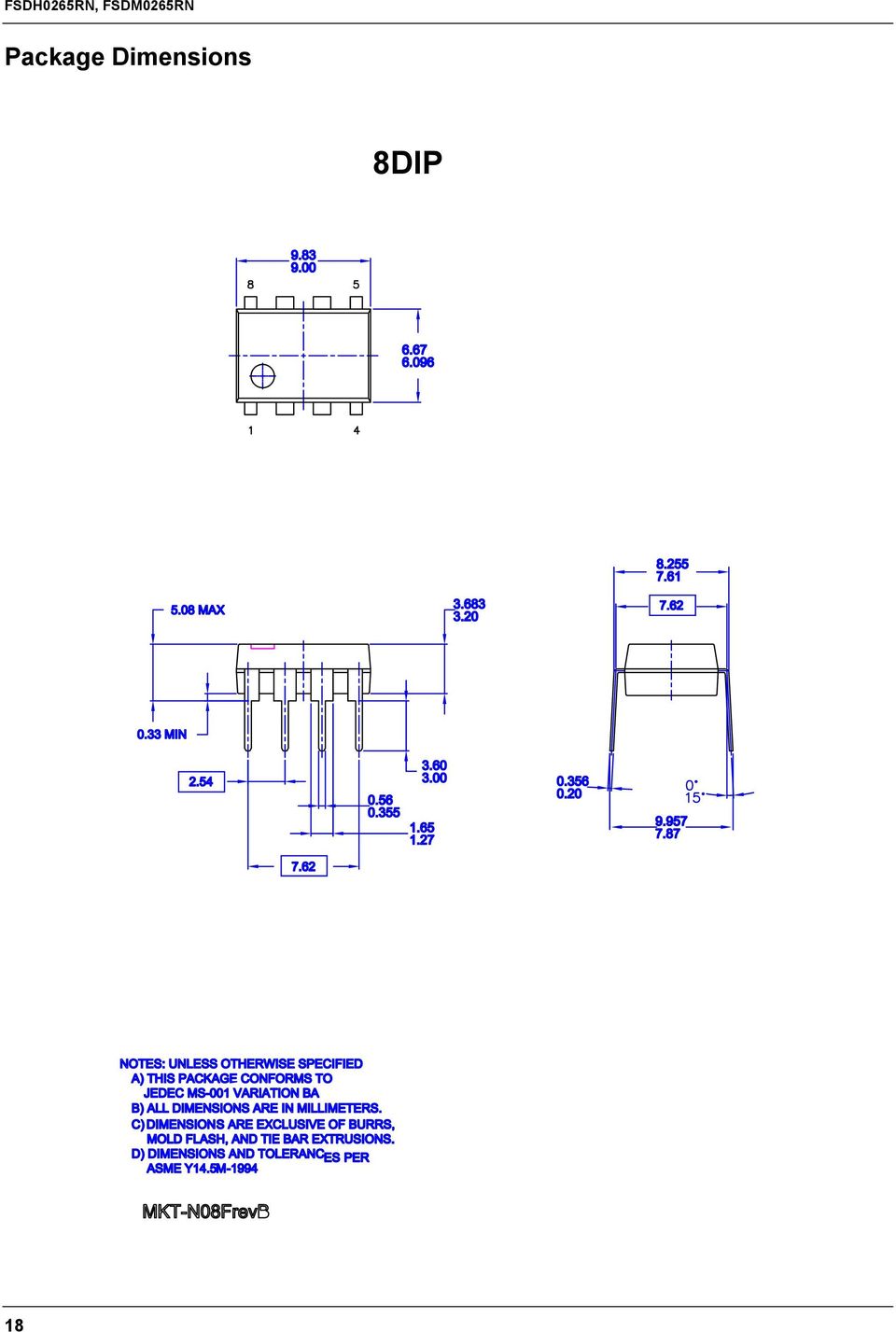
18 Package Dimensions 8DIP 18
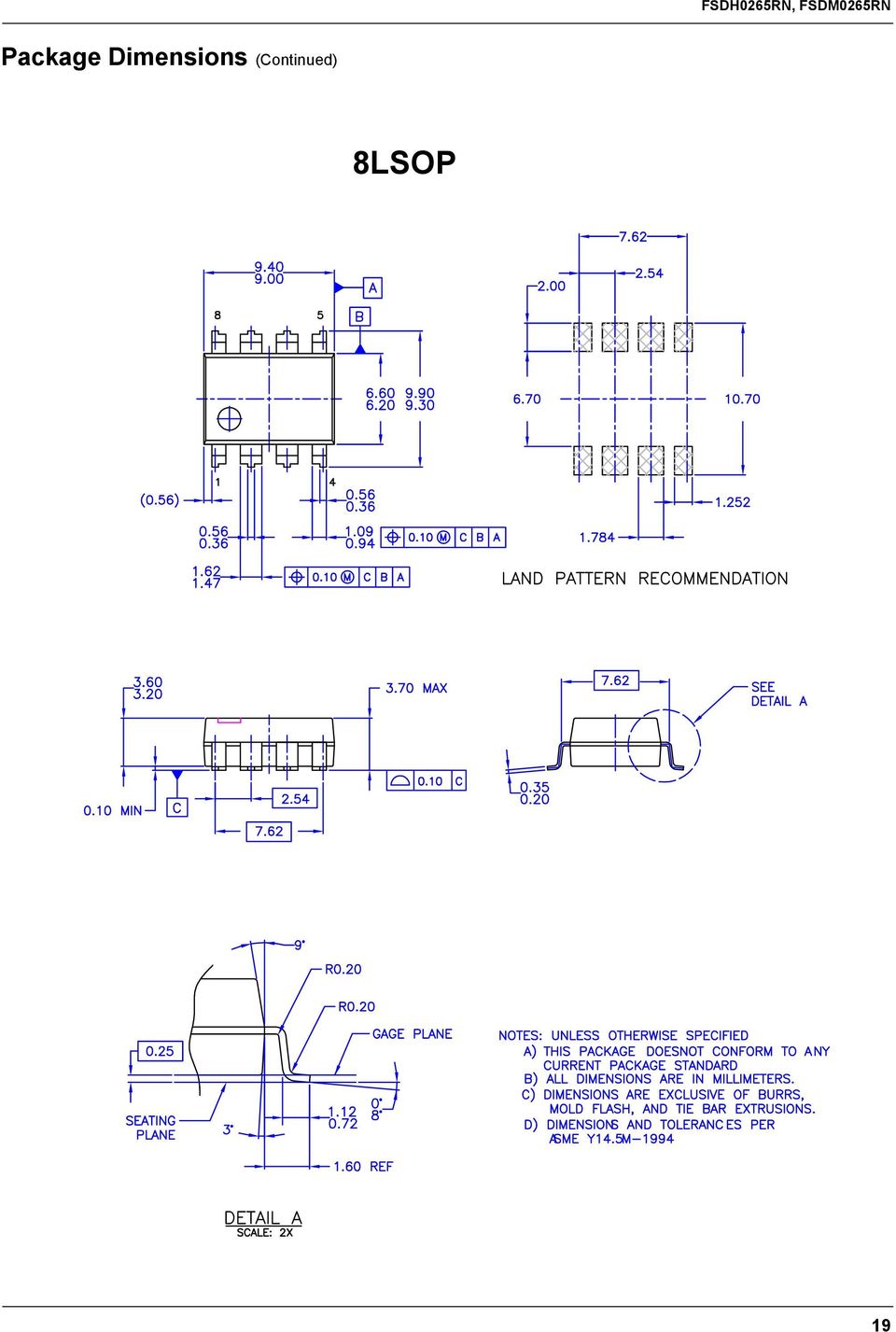
19 Package Dimensions (Continued) 8LSOP 19
20 Ordering Information Product Number Package Marking Code BVDSS fosc RDS(ON) FSDM0265RN 8DIP DM0265R 650V 67KHz 5.0Ω FSDH0265RN 8DIP DH0265R 650V 100KHz 5.0Ω FSDM0265RL 8LSOP DM0265R 650V 67KHz 5.0Ω FSDH0265RL 8LSOP DH0265R 650V 100KHz 5.0Ω DISCLAIMER FAIRCHILD SEMICONDUCTOR RESERVES THE RIGHT TO MAKE CHANGES WITHOUT FURTHER NOTICE TO ANY PRODUCTS HEREIN TO IMPROVE RELIABILITY, FUNCTION OR DESIGN. FAIRCHILD DOES NOT ASSUME ANY LIABILITY ARISING OUT OF THE APPLICATION OR USE OF ANY PRODUCT OR CIRCUIT DESCRIBED HEREIN; NEITHER DOES IT CONVEY ANY LICENSE UNDER ITS PATENT RIGHTS, NOR THE RIGHTS OF OTHERS. LIFE SUPPORT POLICY FAIRCHILD S PRODUCTS ARE NOT AUTHORIZED FOR USE AS CRITICAL COMPONENTS IN LIFE SUPPORT DEVICES OR SYSTEMS WITHOUT THE EXPRESS WRITTEN APPROVAL OF THE PRESIDENT OF FAIRCHILD SEMICONDUCTOR CORPORATION. As used herein: 1. Life support devices or systems are devices or systems which, (a) are intended for surgical implant into the body, or (b) support or sustain life, and (c) whose failure to perform when properly used in accordance with instructions for use provided in the labeling, can be reasonably expected to result in a significant injury of the user. 2. A critical component in any component of a life support device or system whose failure to perform can be reasonably expected to cause the failure of the life support device or system, or to affect its safety or effectiveness. 9/29/05 0.0m Fairchild Semiconductor Corporation

SD4840/4841/4842/4843/4844
 CURRENT MODE PWM CONTROLLER WITH BUILT-IN HIGH VOLTAGE MOSFET DESCRIPTION SD4840/4841/4842/4843/4844 is a current mode PWM controller with low standby power and low start current for power switch. In standby
FSCM0765R. Green Mode Fairchild Power Switch (FPS TM ) Features. Application. Typical Circuit. Description. www.fairchildsemi.com
 Features. Application. Typical Circuit. Description. www.fairchildsemi.com") www.fairchildsemi.com FSCM0765R Green Mode Fairchild Power Switch (FPS TM ) Features Internal Avalanche Rugged Sense FET Low startup current (max 40uA) Low power consumption under 1 W at 240VAC & 0.4W
www.fairchildsemi.com FSCM0765R Green Mode Fairchild Power Switch (FPS TM ) Features Internal Avalanche Rugged Sense FET Low startup current (max 40uA) Low power consumption under 1 W at 240VAC & 0.4W
FSL128MRT Green-Mode Fairchild Power Switch (FPS ) for High Input Voltage
 for High Input Voltage") FSL128MRT Green-Mode Fairchild Power Switch (FPS ) for High Input Voltage Features Internal Avalanched Rugged 800V SenseFET Advanced Soft Burst-Mode Operation for Low Standby Power and Low audible noise
FSL128MRT Green-Mode Fairchild Power Switch (FPS ) for High Input Voltage Features Internal Avalanched Rugged 800V SenseFET Advanced Soft Burst-Mode Operation for Low Standby Power and Low audible noise
UNISONIC TECHNOLOGIES CO., LTD
 UPS61 UNISONIC TECHNOLOGIES CO., LTD HIGH PERFORMANCE CURRENT MODE POWER SWITCH DESCRIPTION The UTC UPS61 is designed to provide several special enhancements to satisfy the needs, for example, Power-Saving
UC3842/UC3843/UC3844/UC3845
 SMPS Controller www.fairchildsemi.com Features Low Start up Current Maximum Duty Clamp UVLO With Hysteresis Operating Frequency up to 500KHz Description The UC3842/UC3843/UC3844/UC3845 are fixed frequencycurrent-mode
KA7500C. SMPS Controller. Features. Description. Internal Block Diagram. www.fairchildsemi.com
 SMPS Controller www.fairchildsemi.com Features Internal Regulator Provides a Stable 5V Reference Supply Trimmed to ±1% Accuracy. Uncommitted Output TR for 200mA Sink or Source Current Output Control for
LD7550-B. Green-Mode PWM Controller. General Description. Features. Applications. Typical Application. REV: 01a 12/22/2006 LD7550-B
 12/22/2006 REV: 01a Green-Mode PWM Controller General Description The LD7550-B is a low cost, low startup current, current mode PWM controller with green-mode power-saving operation. The integrated functions
UNISONIC TECHNOLOGIES CO., LTD UC3863 LINEAR INTEGRATED CIRCUIT
 UNISONIC TECHNOLOGIES CO., LTD UC3863 LOW COST POWER-SAVING MODE PWM CONTROLLER FOR FLYBACK CONVERTERS DESCRIPTION The UC3863 is a high performance current mode PWM controller ideally suited for low standby
Application Note AN4137
 www.fairchildsemi.com Application Note AN4137 Design Guidelines for Offline Flyback Converters Using Fairchild Power Switch (FPS) Abstract This paper presents practical design guidelines for offline flyback
AP1509. 150KHz, 2A PWM BUCK DC/DC CONVERTER. Description. Pin Assignments V IN. Applications. Features. (Top View) GND GND. Output AP1509 GND GND
 GND GND. Output AP1509 GND GND") Description Pin Assignments The series are monolithic IC designed for a stepdown DC/DC converter, and own the ability of driving a 2A load without additional transistor. It saves board space. The external
Description Pin Assignments The series are monolithic IC designed for a stepdown DC/DC converter, and own the ability of driving a 2A load without additional transistor. It saves board space. The external
IRF150 [REF:MIL-PRF-19500/543] 100V, N-CHANNEL. Absolute Maximum Ratings
![IRF150 [REF:MIL-PRF-19500/543] 100V, N-CHANNEL. Absolute Maximum Ratings](/thumbs/40/21333646.jpg "IRF150 [REF:MIL-PRF-19500/543] 100V, N-CHANNEL. Absolute Maximum Ratings") PD - 90337G REPETITIVE AVALANCHE AND dv/dt RATED HEXFET TRANSISTORS THRU-HOLE (TO-204AA/AE) Product Summary Part Number BVDSS RDS(on) ID IRF150 100V 0.055Ω 38A IRF150 JANTX2N6764 JANTXV2N6764 [REF:MIL-PRF-19500/543]
PD - 90337G REPETITIVE AVALANCHE AND dv/dt RATED HEXFET TRANSISTORS THRU-HOLE (TO-204AA/AE) Product Summary Part Number BVDSS RDS(on) ID IRF150 100V 0.055Ω 38A IRF150 JANTX2N6764 JANTXV2N6764 [REF:MIL-PRF-19500/543]
Preliminary Datasheet
 Features Macroblock Preliminary Datasheet 1.2A Constant Output Current 93% Efficiency @ input voltage 13V, 350mA, 9~36V Input Voltage Range Hysteretic PFM Improves Efficiency at Light Loads Settable Output
TDA4605 CONTROL CIRCUIT FOR SWITCH MODE POWER SUPPLIES USING MOS TRANSISTORS
 CONTROL CIRCUIT FOR SWITCH MODE POWER SUPPLIES USING MOS TRANSISTORS Fold-Back Characteristic provides Overload Protection for External Diodes Burst Operation under Short-Circuit and no Load Conditions
FEBFL7701_L30U003A. 2.4W LED Ballast Using FL7701. Featured Fairchild Product: FL7701
 User Guide for FEBFL7701_L30U003A 2.4W LED Ballast Using FL7701 Featured Fairchild Product: FL7701 Direct questions or comments about this evaluation board to: Worldwide Direct Support Fairchild Semiconductor.com
Programmable Single-/Dual-/Triple- Tone Gong SAE 800
 Programmable Single-/Dual-/Triple- Tone Gong Preliminary Data SAE 800 Bipolar IC Features Supply voltage range 2.8 V to 18 V Few external components (no electrolytic capacitor) 1 tone, 2 tones, 3 tones
LM1084 5A Low Dropout Positive Regulators
 5A Low Dropout Positive Regulators General Description The LM1084 is a series of low dropout voltage positive regulators with a maximum dropout of 1.5 at 5A of load current. It has the same pin-out as
FAN7680. PC Power Supply Outputs Monitoring IC. Features. Description. Typical Application. www.fairchildsemi.com FPO OVP UVP PGO PSON
 PC Power Supply Outputs Monitoring IC www.fairchildsemi.com Features PC Power Supply Output Monitor Circuitry Few External Components Over Voltage Protection for.v, V and V(Vcc) Outputs Under Voltage Protection
AN2228 APPLICATION NOTE
 AN2228 APPLICATION NOTE STD1LNK60Z-based Cell Phone Battery Charger Design Introduction This application note is a Ringing Choke Converter (RCC)-based, step-by-step cell phone battery charger design procedure.
LM2704 Micropower Step-up DC/DC Converter with 550mA Peak Current Limit
 Micropower Step-up DC/DC Converter with 550mA Peak Current Limit General Description The LM2704 is a micropower step-up DC/DC in a small 5-lead SOT-23 package. A current limited, fixed off-time control
Power Management & Supply. Design Note. Version 1.0, Nov. 2001 DN-EVALMF2ICE2A265-1. CoolSET 35W DVD Power Supply with ICE2A265.
 Version 1.0, Nov. 2001 Design Note DN-EVALMF2ICE2A265-1 CoolSET 35W DVD Power Supply with ICE2A265 Author: Harald Zöllinger Published by Infineon Technologies AG http://www.infineon.com Power Management
400KHz 60V 4A Switching Current Boost / Buck-Boost / Inverting DC/DC Converter
 Features Wide 5V to 32V Input Voltage Range Positive or Negative Output Voltage Programming with a Single Feedback Pin Current Mode Control Provides Excellent Transient Response 1.25V reference adjustable
MP2259 1A, 16V, 1.4MHz Step-Down Converter
 MP59 1A, 1V, 1.MHz Step-Down Converter TM The Future of Analog IC Technology DESCRIPTION The MP59 is a monolithic integrated stepdown switch mode converter with an internal power MOSFET. It achieves 1A
LDS8720. 184 WLED Matrix Driver with Boost Converter FEATURES APPLICATION DESCRIPTION TYPICAL APPLICATION CIRCUIT
 184 WLED Matrix Driver with Boost Converter FEATURES High efficiency boost converter with the input voltage range from 2.7 to 5.5 V No external Schottky Required (Internal synchronous rectifier) 250 mv
Series AMLDL-Z Up to 1000mA LED Driver
 FEATURES: Click on Series name for product info on aimtec.com Series Up to ma LED Driver Models Single output Model Input Voltage (V) Step Down DC/DC LED driver Operating Temperature range 4ºC to 85ºC
unit : mm With heat sink (see Pd Ta characteristics)
") Ordering number: EN1321E Monolithic Linear IC LA4261 3.5 W 2-Channel AF Power Amplifier for Home Stereos and Music Centers Features. Minimum number of external parts required (No input capacitor, bootstrap
Ordering number: EN1321E Monolithic Linear IC LA4261 3.5 W 2-Channel AF Power Amplifier for Home Stereos and Music Centers Features. Minimum number of external parts required (No input capacitor, bootstrap
N-channel enhancement mode TrenchMOS transistor
 FEATURES SYMBOL QUICK REFERENCE DATA Trench technology d V DSS = V Low on-state resistance Fast switching I D = A High thermal cycling performance Low thermal resistance R DS(ON) mω (V GS = V) g s R DS(ON)
AP1510. General Description. Features. Applications. Typical Application Circuit PWM CONTROL 3A STEP-DOWN CONVERTER AP1510. x (1+R A = V FB /R B
 Features General Description Input voltage: 3.6 to 23 Output voltage: 0.8 to CC. Duty ratio: 0% to 100% PWM control Oscillation frequency: 300kHz typ. Current Limit, Enable function Thermal Shutdown function
FAN5346 Series Boost LED Driver with PWM Dimming Interface
 FAN5346 Series Boost LED Driver with PWM Dimming Interface Features Asynchronous Boost Converter Drives LEDs in Series: FAN5346S20X: 20V Output FAN5346S30X: 30V Output 2.5V to 5.5V Input Voltage Range
PAM2804. Pin Assignments. Description. Applications. Features. Typical Applications Circuit 1A STEP-DOWN CONSTANT CURRENT, HIGH EFFICIENCY LED DRIVER
 1A STEP-DOWN CONSTANT CURRENT, HIGH EFFICIENCY LED DRIER Description Pin Assignments The is a step-down constant current LED driver. When the input voltage is down to lower than LED forward voltage, then
Switching Regulators. STR-A6169 Universal-Input/5 W Flyback Switching Regulator FUNCTIONAL BLOCK DIAGRAM
 ABSOLUTE MAXIMUM RATINGS at T A = +25 C Control Supply Voltage, V CC.... 35 V Drain-Source Voltage, V DSS...... 800 V Drain Switching Current, I D.... 1.2 A* Peak Drain Switching Current, I DM.................................
High Performance Current Mode PWM Controller Cycle Turning + POWER FROM LIEMIC. For, 2008 LIEMIC Semiconductor Co.,Ltd. LN3C63AD REV: 1.0.
 LN3C63 High Performance Current Mode PWM Controller Cycle Turning + POWER FROM LIEMIC For, Adaptor & Charger Offline Power Supply Open Frame Power DVD&DVB Player Auxiliary Power for PC etc..... 2008 LIEMIC
LM5001 High Voltage Switch Mode Regulator
 High Voltage Switch Mode Regulator General Description The LM5001 high voltage switch mode regulator features all of the functions necessary to implement efficient high voltage Boost, Flyback, SEPIC and
www.jameco.com 1-800-831-4242
 Distributed by: www.jameco.com 1-800-831-4242 The content and copyrights of the attached material are the property of its owner. LF411 Low Offset, Low Drift JFET Input Operational Amplifier General Description
SG2525A SG3525A REGULATING PULSE WIDTH MODULATORS
 SG2525A SG3525A REGULATING PULSE WIDTH MODULATORS 8 TO 35 V OPERATION 5.1 V REFERENCE TRIMMED TO ± 1 % 100 Hz TO 500 KHz OSCILLATOR RANGE SEPARATE OSCILLATOR SYNC TERMINAL ADJUSTABLE DEADTIME CONTROL INTERNAL
1ED Compact A new high performance, cost efficient, high voltage gate driver IC family
 1ED Compact A new high performance, cost efficient, high voltage gate driver IC family Heiko Rettinger, Infineon Technologies AG, Am Campeon 1-12, 85579 Neubiberg, Germany, [email protected]
Symbol Parameter Value Unit IAR Avalanche Current, Repetitive or Not-Repetitive
 BUZ11 N - CHANNEL 50V - 0.03Ω - 30A -TO-220 STripFET POWER MOSFET TYPE V DSS R DS(on) I D BUZ11 50 V < 0.04 Ω 30 A TYPICAL R DS(on) = 0.03 Ω AVALANCHE RUGGED TECHNOLOGY 100% AVALANCHE TESTED HIGH CURRENT
FPAB20BH60B PFC SPM 3 Series for Single-Phase Boost PFC
 FPAB20BH60B PFC SPM 3 Series for Single-Phase Boost PFC Features UL Certified No. E209204 (UL1557) 600 V - 20 A Single-Phase Boost PFC with Integral Gate Driver and Protection Very Low Thermal Resistance
STP6N60FI N - CHANNEL ENHANCEMENT MODE POWER MOS TRANSISTOR
 N - CHANNEL ENHANCEMENT MODE POWER MOS TRANSISTOR TYPE VDSS RDS(on) ID STP6N60FI 600 V < 1.2 Ω 3.8 A TYPICAL R DS(on) =1Ω AVALANCHE RUGGED TECHNOLOGY 100% AVALANCHE TESTED REPETITIVE AVALANCHE DATA AT
AP1506. 150KHz, 3A PWM BUCK DC/DC CONVERTER. Pin Assignments. Description. Features. Applications. ( Top View ) 5 SD 4 FB 3 Gnd 2 Output 1 V IN
 5 SD 4 FB 3 Gnd 2 Output 1 V IN") Description Pin Assignments The series are monolithic IC designed for a stepdown DC/DC converter, and own the ability of driving a 3A load without external transistor. Due to reducing the number of external
Description Pin Assignments The series are monolithic IC designed for a stepdown DC/DC converter, and own the ability of driving a 3A load without external transistor. Due to reducing the number of external
SWITCH-MODE POWER SUPPLY CONTROLLER PULSE OUTPUT DC OUTPUT GROUND EXTERNAL FUNCTION SIMULATION ZERO CROSSING INPUT CONTROL EXTERNAL FUNCTION
 SWITCH-MODE POWER SUPPLY CONTROLLER. LOW START-UP CURRENT. DIRECT CONTROL OF SWITCHING TRAN- SISTOR. COLLECTOR CURRENT PROPORTIONAL TO BASE-CURRENT INPUT REERSE-GOING LINEAR OERLOAD CHARACTERISTIC CURE
AC/DC Power Management Devices. 2015 Product Guide. AC/DC Control ICs with integrated MOSFETs in LLC, QR & PWM Topologies
 AC/DC Power Management Devices 2015 Product Guide AC/DC Control ICs with integrated MOSFETs in LLC, QR & PWM Topologies About Us Headquarters Japan Sanken Electric Co., Ltd. is a Japanese company who s
AND8480/D. CrM Buck LED Driver Evaluation Board APPLICATION NOTE
 CrM Buck LED Driver Evaluation Board Prepared by: Fabien Franc ON Semiconductor Introduction This document describes the CrM Buck LED driver evaluation board. This board provides a step down converter
Push-Pull FET Driver with Integrated Oscillator and Clock Output
 19-3662; Rev 1; 5/7 Push-Pull FET Driver with Integrated Oscillator General Description The is a +4.5V to +15V push-pull, current-fed topology driver subsystem with an integrated oscillator for use in
BUZ11. 30A, 50V, 0.040 Ohm, N-Channel Power MOSFET. Features. [ /Title (BUZ1 1) /Subject. (30A, 50V, 0.040 Ohm, N- Channel. Ordering Information
 /Subject. (30A, 50V, 0.040 Ohm, N- Channel. Ordering Information") Data Sheet June 1999 File Number 2253.2 [ /Title (BUZ1 1) /Subject (3A, 5V,.4 Ohm, N- Channel Power MOS- FET) /Autho r () /Keywords (Intersil Corporation, N- Channel Power MOS- FET, TO- 22AB ) /Creator
Data Sheet June 1999 File Number 2253.2 [ /Title (BUZ1 1) /Subject (3A, 5V,.4 Ohm, N- Channel Power MOS- FET) /Autho r () /Keywords (Intersil Corporation, N- Channel Power MOS- FET, TO- 22AB ) /Creator
Features. TA=25 o C unless otherwise noted
 NDSAN N-Channel, Logic Level, PowerTrench MOSFET June NDSAN General Description These N-Channel Logic Level MOSFETs are produced using Fairchild Semiconductor s advanced PowerTrench process that has been
AP3125A/V/L/R. Description. Pin Assignments NEW PRODUCT. Features. Applications. A Product Line of. Diodes Incorporated GREEN MODE PWM CONTROLLER
 Description Pin Assignments GREEN MODE PWM CONTROLLER The is a current mode PWM controller which is optimized for high performance, low standby power and cost effective offline flyback converters. (Top
Design Considerations for an LLC Resonant Converter
 Design Considerations for an LLC Resonant Converter Hangseok Choi Power Conversion Team www.fairchildsemi.com 1. Introduction Growing demand for higher power density and low profile in power converter
Lower Conduction Losses Low Thermal Resistance to PCB ( 0.5 C/W)
") PD -97428 IRFH5020PbF HEXFET Power MOSFET V DS 200 V 55 m: R DS(on) max (@V GS = V) Q g (typical) 36 nc R G (typical).9 : I D (@T c(bottom) = 25 C) 43 A PQFN 5X6 mm Applications Secondary Side Synchronous
PD -97428 IRFH5020PbF HEXFET Power MOSFET V DS 200 V 55 m: R DS(on) max (@V GS = V) Q g (typical) 36 nc R G (typical).9 : I D (@T c(bottom) = 25 C) 43 A PQFN 5X6 mm Applications Secondary Side Synchronous
TSM2N7002K 60V N-Channel MOSFET
 SOT-23 SOT-323 Pin Definition: 1. Gate 2. Source 3. Drain PRODUCT SUMMARY V DS (V) R DS(on) (Ω) I D (ma) 5 @ V GS = 10V 100 60 5.5 @ V GS = 5V 100 Features Low On-Resistance ESD Protection High Speed Switching
Cool-Power PI33xx-x0. 8 V to 36 V IN Cool-Power ZVS Buck Regulator Family. Product Description. Features & Benefits. Applications. Package Information
 Cool-Power PI33xx-x0 8 V to 36 V IN Cool-Power ZVS Buck Regulator Family Product Description The PI33xx-x0 is a family of high efficiency, wide input range DC-DC ZVS-Buck regulators integrating controller,
Datasheet. 2A 380KHZ 20V PWM Buck DC/DC Converter. Features
 General Description Features The is a 380 KHz fixed frequency monolithic step down switch mode regulator with a built in internal Power MOSFET. It achieves 2A continuous output current over a wide input
HV start-up DCM/QR flyback controller with integrated DCM/QR PFC controller
 HV start-up DCM/QR flyback with integrated DCM/QR PFC Rev. 1.1 13 March 2015 Product data sheet 1. General description The GreenChip is the latest generation of green Switched Mode Power Supply (SMPS)
TLI4946. Datasheet TLI4946K, TLI4946-2K, TLI4946-2L. Sense and Control. May 2009
 May 2009 TLI4946 High Precision Hall Effect Latches for Industrial and Consumer Applications TLI4946K, TLI4946-2K, TLI4946-2L Datasheet Rev. 1.0 Sense and Control Edition 2009-05-04 Published by Infineon
IRLR8729PbF IRLU8729PbF
 Applications l High Frequency Synchronous Buck Converters for Computer Processor Power l High Frequency Isolated DC-DC Converters with Synchronous Rectification for Telecom and Industrial Use Benefits
PHOTOTRANSISTOR OPTOCOUPLERS
 MCT2 MCT2E MCT20 MCT27 WHITE PACKAGE (-M SUFFIX) BLACK PACKAGE (NO -M SUFFIX) DESCRIPTION The MCT2XXX series optoisolators consist of a gallium arsenide infrared emitting diode driving a silicon phototransistor
AAT4280 Slew Rate Controlled Load Switch
 General Description Features SmartSwitch The AAT4280 SmartSwitch is a P-channel MOSFET power switch designed for high-side load switching applications. The P-channel MOSFET device has a typical R DS(ON)
OptiMOS 3 Power-Transistor
 Type IPD36N4L G OptiMOS 3 Power-Transistor Features Fast switching MOSFET for SMPS Optimized technology for DC/DC converters Qualified according to JEDEC ) for target applications Product Summary V DS
CAT4101TV. 1 A Constant-Current LED Driver with PWM Dimming
 A Constant-Current LED Driver with PWM Dimming Description The CAT4 is a constant current sink driving a string of high brightness LEDs up to A with very low dropout of.5 V at full load. It requires no
28V, 2A Buck Constant Current Switching Regulator for White LED
 28V, 2A Buck Constant Current Switching Regulator for White LED FP7102 General Description The FP7102 is a PWM control buck converter designed to provide a simple, high efficiency solution for driving
Features 1.7 A, 20 V. R DS(ON) Symbol Parameter Ratings Units
 Symbol Parameter Ratings Units") N-Channel.5V Specified PowerTrench TM MOSFET April 999 General Description This N-Channel.5V specified MOSFET is produced using Fairchild Semiconductor's advanced PowerTrench process that has been especially
N-Channel.5V Specified PowerTrench TM MOSFET April 999 General Description This N-Channel.5V specified MOSFET is produced using Fairchild Semiconductor's advanced PowerTrench process that has been especially
.OPERATING SUPPLY VOLTAGE UP TO 46 V
 L298 DUAL FULL-BRIDGE DRIVER.OPERATING SUPPLY VOLTAGE UP TO 46 V TOTAL DC CURRENT UP TO 4 A. LOW SATURATION VOLTAGE OVERTEMPERATURE PROTECTION LOGICAL "0" INPUT VOLTAGE UP TO 1.5 V (HIGH NOISE IMMUNITY)
SPI-8001TW. Switching Regulators. Dual 1.5 A, DC/DC Step-Down Converter. SANKEN ELECTRIC CO., LTD. http://www.sanken-ele.co.jp/en/
 Data Sheet 27469.301.1 Designed to meet high-current requirements at high efficiency in industrial and consumer applications; embedded core, memory, or logic supplies; TVs, VCRs, and office equipment,
S112-XHS. Description. Features. Agency Approvals. Applications. Absolute Maximum Ratings. Schematic Diagram. Ordering Information
 Description Features The S112-X is a bi-directional, single-pole, single-throw, normally open multipurpose solid-state relay. The circuit is composed of one input IR LED with a series limiting resistor
AUIPS71411G CURRENT SENSE HIGH SIDE SWITCH
 February, 21st 2010 Automotive grade AUIPS71411G CURRENT SENSE HIGH SIDE SWITCH Features Suitable 24V battery operation Over current shutdown Over temperature shutdown Current sensing Active clamp Low
AS2815. 1.5A Low Dropout Voltage Regulator Adjustable & Fixed Output, Fast Response
 1.5A Low Dropout oltage Regulator Adjustable & Fixed Output, Fast Response FEATURES Adjustable Output Down To 1.2 Fixed Output oltages 1.5, 2.5, 3.3, 5.0 Output Current of 1.5A Low Dropout oltage 1.1 Typ.
LM78XX Series Voltage Regulators
 LM78XX Series Voltage Regulators General Description Connection Diagrams The LM78XX series of three terminal regulators is available with several fixed output voltages making them useful in a wide range
LM2576R. 3.0A, 52kHz, Step-Down Switching Regulator FEATURES. Applications DESCRIPTION TO-220 PKG TO-220V PKG TO-263 PKG ORDERING INFORMATION
 LM2576 FEATURES 3.3, 5.0, 12, 15, and Adjustable Output ersions Adjustable ersion Output oltage Range, 1.23 to 37 +/- 4% AG10Maximum Over Line and Load Conditions Guaranteed 3.0A Output Current Wide Input
Simple PWM Boost Converter with I/O Disconnect Solves Malfunctions Caused when V OUT <V IN
 Simple PWM Boost Converter with I/O Disconnect Solves Malfunctions Caused when V OUT
CAT4139. 22 V High Current Boost White LED Driver
 22 V High Current Boost White LED Driver Description The CAT4139 is a DC/DC step up converter that delivers an accurate constant current ideal for driving LEDs. Operation at a fixed switching frequency
Pulse Width Modulation Amplifiers EQUIVALENT CIRCUIT DIAGRAM. 200mV + - SMART CONTROLLER .01F OSC Q3. 2200pF
 Pulse Width Modulation Amplifiers MSA MSA FEATURES LOW COST HIGH VOLTAGE VOLTS HIGH OUTPUT CURRENT AMPS kw OUTPUT CAPABILITY VARIABLE SWITCHING FREQUEY APPLICATIONS BRUSH MOTOR CONTROL MRI MAGNETIC BEARINGS
AND8147/D. An Innovative Approach to Achieving Single Stage PFC and Step-Down Conversion for Distributive Systems APPLICATION NOTE
 An Innovative Approach to Achieving Single Stage PFC and Step-Down Conversion for Distributive Systems APPLICATION NOTE INTRODUCTION In most modern PFC circuits, to lower the input current harmonics and
IS32BL3554 BOOST TYPE LED DRIVER WITH 4-CHANNEL CURRENT SOURCE
 ISBL BOOST TYPE LED DRIVER WITH -CHANNEL CURRENT SOURCE DESCRIPTION The ISBL is a white LED driver for backlight applications based on a highly efficient boost controller operating over a wide input voltage
LM118/LM218/LM318 Operational Amplifiers
 LM118/LM218/LM318 Operational Amplifiers General Description The LM118 series are precision high speed operational amplifiers designed for applications requiring wide bandwidth and high slew rate. They
IRF830. N - CHANNEL 500V - 1.35Ω - 4.5A - TO-220 PowerMESH MOSFET
 IRF830 N - CHANNEL 500V - 1.35Ω - 4.5A - TO-220 PowerMESH MOSFET TYPE V DSS R DS(on) I D IRF830 500 V < 1.5 Ω 4.5 A TYPICAL R DS(on) = 1.35 Ω EXTREMELY HIGH dv/dt CAPABILITY 100% AVALANCHE TESTED VERY
Understanding the Terms and Definitions of LDO Voltage Regulators
 Application Report SLVA79 - October 1999 Understanding the Terms and Definitions of ltage Regulators Bang S. Lee Mixed Signal Products ABSTRACT This report provides an understanding of the terms and definitions
How To Make A Field Effect Transistor (Field Effect Transistor) From Silicon P Channel (Mos) To P Channel Power (Mos) (M2) (Mm2)
 From Silicon P Channel (Mos) To P Channel Power (Mos) (M2) (Mm2)") TPC811 TOSHIBA Field Effect Transistor Silicon P Channel MOS Type (U-MOS III) TPC811 Lithium Ion Battery Applications Notebook PC Applications Portable Equipment Applications Unit: mm Small footprint due
TPC811 TOSHIBA Field Effect Transistor Silicon P Channel MOS Type (U-MOS III) TPC811 Lithium Ion Battery Applications Notebook PC Applications Portable Equipment Applications Unit: mm Small footprint due
29V High Voltage LED Driver
 29V High Voltage LED Driver SP7601 FEATURES Wide Input Voltage Range 4.5V 29V 1.2MHz Constant Frequency Operation Low 0.2V Reference Voltage Adjustable Overcurrent Protection PWM Dimming and Power sequencing
Equivalent Circuit. Operating Characteristics at Ta = 25 C, V CC = ±34V, R L = 8Ω, VG = 40dB, Rg = 600Ω, R L : non-inductive load STK4181V
 Ordering number: 2137B Thick Film Hybrid IC STK4181V AF Power Amplifier (Split Power Supply) (45W + 45W min, THD = 0.08%) Features Pin-compatible with the STK4102II series. The STK4101V series use the
DC/DC power modules basics
 DC/DC power modules basics Design Note 024 Ericsson Power Modules General Abstract This design note covers basic considerations for the use of on-board switch mode DC/DC power modules, also commonly known
MIC33050. General Description. Features. Applications. Typical Application. 4MHz Internal Inductor PWM Buck Regulator with HyperLight Load
 4MHz Internal Inductor PWM Buck Regulator with HyperLight Load General Description The Micrel is a high-efficiency 600mA PWM synchronous buck (step-down) regulator with internal inductor featuring HyperLight
UNISONIC TECHNOLOGIES CO., LTD 50N06 Power MOSFET
 UNISONIC TECHNOLOGIES CO., LTD 50N06 50 Amps, 60 Volts N-CHANNEL POWER MOSFET DESCRIPTION TO-263 TO-25 The UTC 50N06 is three-terminal silicon device with current conduction capability of about 50A, fast
MP2456 0.5A, 50V, 1.2MHz Step-Down Converter in a TSOT23-6
 MP2456 0.5A, 50V, 1.2MHz Step-Down Converter in a TSOT23-6 DESCRIPTION The MP2456 is a monolithic, step-down, switchmode converter with a built-in power MOSFET. It achieves a 0.5A peak-output current over
MP2365 3A, 28V, 1.4MHz Step-Down Converter
 The Future of Analog IC Technology MP365 3A, 8,.MHz Step-Down Converter DESCRIPTION The MP365 is a.mhz step-down regulator with a built-in Power MOSFET. It achieves 3A continuous output current over a
Features. Symbol JEDEC TO-220AB
 Data Sheet June 1999 File Number 2253.2 3A, 5V,.4 Ohm, N-Channel Power MOSFET This is an N-Channel enhancement mode silicon gate power field effect transistor designed for applications such as switching
FAN8082 (KA3082N) Bi-directional DC Motor Driver. Features. Description. Typical Applications. Ordering Information. www.fairchildsemi.
 Bi-directional DC Motor Driver. Features. Description. Typical Applications. Ordering Information. www.fairchildsemi.") Bi-directional DC Motor Driver www.fairchildsemi.com Features Built-in brake function for stable brake characteristics. Built-in element to absorb a surge current derived from changing motor direction
Bi-directional DC Motor Driver www.fairchildsemi.com Features Built-in brake function for stable brake characteristics. Built-in element to absorb a surge current derived from changing motor direction
FSEZ1307 Primary-Side-Regulation PWM with Power MOSFET Integrated
 January 2014 FSEZ1307 Primary-Side-Regulation PWM with Power MOSFET Integrated Features Low Standby Power: Under 30 mw High-Voltage Startup Few External Components Constant-Voltage (CV) and Constant-Current
MM74C150 MM82C19 16-Line to 1-Line Multiplexer 3-STATE 16-Line to 1-Line Multiplexer
 MM74C150 MM82C19 16-Line to 1-Line Multiplexer 3-STATE 16-Line to 1-Line Multiplexer General Description The MM74C150 and MM82C19 multiplex 16 digital lines to 1 output. A 4-bit address code determines
LM138 LM338 5-Amp Adjustable Regulators
 LM138 LM338 5-Amp Adjustable Regulators General Description The LM138 series of adjustable 3-terminal positive voltage regulators is capable of supplying in excess of 5A over a 1 2V to 32V output range
LM386 Low Voltage Audio Power Amplifier
 Low Voltage Audio Power Amplifier General Description The LM386 is a power amplifier designed for use in low voltage consumer applications. The gain is internally set to 20 to keep external part count
N-Channel 20-V (D-S) 175 C MOSFET
 175 C MOSFET") N-Channel -V (D-S) 75 C MOSFET SUD7N-4P PRODUCT SUMMARY V DS (V) r DS(on) ( ) (A) a.37 @ V GS = V 37.6 @ V GS = 4.5 V 9 TO-5 D FEATURES TrenchFET Power MOSFET 75 C Junction Temperature PWM Optimized for
N-Channel -V (D-S) 75 C MOSFET SUD7N-4P PRODUCT SUMMARY V DS (V) r DS(on) ( ) (A) a.37 @ V GS = V 37.6 @ V GS = 4.5 V 9 TO-5 D FEATURES TrenchFET Power MOSFET 75 C Junction Temperature PWM Optimized for
Supply voltage Supervisor TL77xx Series. Author: Eilhard Haseloff
 Supply voltage Supervisor TL77xx Series Author: Eilhard Haseloff Literature Number: SLVAE04 March 1997 i IMPORTANT NOTICE Texas Instruments (TI) reserves the right to make changes to its products or to
0.185 (4.70) 0.170 (4.31) 0.055 (1.39) 0.045 (1.14) Features 0.603 (15.32) 0.573 (14.55) 0.104 (2.64) 0.094 (2.39)
 0.170 (4.31) 0.055 (1.39) 0.045 (1.14) Features 0.603 (15.32) 0.573 (14.55) 0.104 (2.64) 0.094 (2.39)") *.6 (4.6).9 (2.28).25 (5.2).9 (4.83).45 (.54) Max..4 (.4).35 (8.89).54 (3.9).42 (3.6) ia. PIN S.48 (29.6).8 (28.4) * May be notched or flat.3 (2.87).2 (2.56).635 (6.3).58 (4.73).37 (.94).26 (.66).5 (2.67).95
*.6 (4.6).9 (2.28).25 (5.2).9 (4.83).45 (.54) Max..4 (.4).35 (8.89).54 (3.9).42 (3.6) ia. PIN S.48 (29.6).8 (28.4) * May be notched or flat.3 (2.87).2 (2.56).635 (6.3).58 (4.73).37 (.94).26 (.66).5 (2.67).95
NCP1612. Enhanced, High-Efficiency Power Factor Controller
 Enhanced, High-Efficiency Power Factor Controller The NCP1612 is designed to drive PFC boost stages based on an innovative Current Controlled Frequency Fold back (CCFF) method. In this mode, the circuit
SELF-OSCILLATING HALF-BRIDGE DRIVER
 Data Sheet No. PD60029 revj I2155&(PbF) (NOTE: For new designs, we recommend I s new products I2153 and I21531) SELF-OSCILLATING HALF-BIDGE DIE Features Floating channel designed for bootstrap operation
Altoran Chip & Systems ACS1004 ACS1004. Compact Direct AC Line LED Driver with high PF and low THD using Only Two External Components FEATURES
 ACS1004 Compact Direct AC Line LED Driver with high PF and low THD using Only Two External Components FEATURES AC Mains Direct LED Driver with Only Two External Components Wide AC Input Range : 90~280VAC
IR1168S DUAL SMART RECTIFIER DRIVER IC
 Datasheet No PD97382 September 26, 2011 IR1168S DUAL SMART RECTIFIER DRIVER IC Features Secondary-side high speed controller for synchronous rectification in resonant half bridge topologies 200V proprietary
DATA SHEET. TDA8560Q 2 40 W/2 Ω stereo BTL car radio power amplifier with diagnostic facility INTEGRATED CIRCUITS. 1996 Jan 08
 INTEGRATED CIRCUITS DATA SHEET power amplifier with diagnostic facility Supersedes data of March 1994 File under Integrated Circuits, IC01 1996 Jan 08 FEATURES Requires very few external components High
Constant Voltage and Constant Current Controller for Adaptors and Battery Chargers
 TECHNICAL DATA Constant Voltage and Constant Current Controller for Adaptors and Battery Chargers IK3051 Description IK3051 is a highly integrated solution for SMPS applications requiring constant voltage
SMPS MOSFET. V DSS R DS (on) max I D
 max I D") Applications l Switch Mode Power Supply (SMPS) l Uninterruptable Power Supply l High speed power switching SMPS MOSFET PD 93773A IRF820A HEXFET Power MOSFET V DSS R DS (on) max I D 500V 3.0Ω 2.5A Benefits
Applications l Switch Mode Power Supply (SMPS) l Uninterruptable Power Supply l High speed power switching SMPS MOSFET PD 93773A IRF820A HEXFET Power MOSFET V DSS R DS (on) max I D 500V 3.0Ω 2.5A Benefits
Power MOSFET. IRF510PbF SiHF510-E3 IRF510 SiHF510. PARAMETER SYMBOL LIMIT UNIT Drain-Source Voltage V DS 100 V Gate-Source Voltage V GS ± 20
 Power MOSFET PRODUCT SUMMARY (V) 100 R DS(on) () = 0.54 Q g max. (nc) 8.3 Q gs (nc) 2.3 Q gd (nc) 3.8 Configuration Single D TO220AB G FEATURES Dynamic dv/dt rating Available Repetitive avalanche rated