FSCM0765R. Green Mode Fairchild Power Switch (FPS TM ) Features. Application. Typical Circuit. Description.
|
|
|
- Cuthbert Collins
- 7 years ago
- Views:
Transcription
1 FSCM0765R Green Mode Fairchild Power Switch (FPS TM ) Features Internal Avalanche Rugged Sense FET Low startup current (max 40uA) Low power consumption under 1 W at 240VAC & 0.4W load Precise Fixed Operating Frequency (66kHz) Frequency Modulation for low EMI Pulse by Pulse Current Limiting (Adjustable) Over Voltage Protection (OVP) Over Load Protection (OLP) Thermal Shutdown Function (TSD) Auto-Restart Mode Under Voltage Lock Out (UVLO) with hysteresis Built-in Soft Start (15ms) Application SMPS for VCR, SVR, STB, DVD & DVCD Adaptor SMPS for LCD Monitor Description Table 1. Maximum Output Power OUTPUT POWER TABLE 230VAC ±15% (3) VAC PRODUCT Adapter Open Adapt- Open (1) Frame (2) er (1) Frame (2) FSCM0565RD 50W 65W 40W 50W FSCM0765RD 65W 70W 50W 60W FSCM0565RC 70W 85W 60W 70W FSCM0765RC 85W 95W 70W 85W Notes: 1. Typical continuous power in a non-ventilated enclosed adapter measured at 50 C ambient. 2. Maximum practical continuous power in an open frame design at 50 C ambient VAC or 100/115 VAC with doubler. Typical Circuit The FSCM0765R is an integrated Pulse Width Modulator (PWM) and Sense FET specifically designed for high performance offline Switch Mode Power Supplies (SMPS) with minimal external components. This device is an integrated high voltage power switching regulator which combine an avalanche rugged Sense FET with a current mode PWM control block. The PWM controller includes integrated fixed frequency oscillator, under voltage lockout, leading edge blanking (LEB), optimized gate driver, internal soft start, temperature compensated precise current sources for a loop compensation and self protection circuitry. Compared with discrete MOSFET and PWM controller solution, it can reduce total cost, component count, size and weight simultaneously increasing efficiency, productivity, and system reliability. This device is a basic platform well suited for cost effective designs of flyback converters. AC IN Drain PWM I limit Vfb Vcc GND Figure 1. Typical Flyback Application DC OUT Rev Fairchild Semiconductor Corporation

2 Internal Block Diagram Vcc Drain /0.5V + 8V/12V Vcc good Vref Internal Bias - Freq. Modulation Vcc Vcc OSC FB I limit 4 5 I delay 0.3K I FB 2.5R Soft start R PWM S R Q Q LEB Gate driver V SD Vcc Vovp TSD Vcc good S R Q Q 2 GND Vcc UV reset Figure 2. Functional Block Diagram of FSCM0765R 2

3 Pin Definitions Pin Number Pin Name Pin Function Description 1 Drain This pin is the high voltage power SenseFET drain. It is designed to drive the transformer directly. 2 GND This pin is the control ground and the SenseFET source. 3 Vcc 4 Feedback (FB) 5 I_limit This pin is the positive supply voltage input. Initially, During start up, the power is supplied through the startup resistor from DC link. When Vcc reaches 12V, the power is supplied from auxiliary transformer winding. This pin is internally connected to the inverting input of the PWM comparator. The collector of an optocoupler is typically tied to this pin. For stable operation, a capacitor should be placed between this pin and GND. If the voltage of this pin reaches 6.0V, the over load protection is activated resulting in shutdown of the FPS. This pin is for the pulse by pulse current limit level programming. By using a resistor to GND on this pin, the current limit level can be changed. If this pin is left floating, the typical current limit will be 3.0A. Pin Configuration FSCM0765RD D2-PAK-5L FSCM0765RC TO-220-5L FSCM0765RD 5 : I_limit 4 : FB 3 : Vcc 2 : GND 1 : Drain FSCM0765RC 5. I_limit 4. FB 3. Vcc 2. GND 1. Drain Figure 3. Pin Configuration (Top View) 3

4 Absolute Maximum Ratings (Ta=25 C, unless otherwise specified) Parameter Symbol Value Unit Drain-Source (GND) Voltage (1) VDSS 650 V Drain-Gate Voltage (RGS=1MΩ) VDGR 650 V Gate-Source (GND) Voltage VGS ±30 V Drain Current Pulsed (2) IDM 28 ADC Single Pulsed Avalanch Energy (3) EAS 370 mj Avalanch Current (4) IAS 35 A Continuous Drain Current (Tc = 25 C) ID 7 ADC Continuous Drain Current (TC=100 C) ID 4.5 ADC Supply Voltage VCC 20 V Analog Input Voltage Range VFB -0.3 to VCC V Total Power Dissipation (D2-PAK) PD 83 W Derating W/ C Total Power Dissipation (TO-220) PD 145 W Derating W/ C Operating Junction Temperature TJ Internally limited C Operating Ambient Temperature TA -25 to +85 C Storage Temperature Range TSTG -55 to +150 C Notes: 1. Tj = 25 C to 150 C 2. Repetitive rating: Pulse width limited by maximum junction temperature 3. L = 30mH, VDD = 50V, RG = 25Ω, starting Tj = 25 C 4. L = 13uH, starting Tj = 25 C 4

5 Electrical Characteristics (Ta = 25 C unless otherwise specified) Parameter Symbol Condition Min. Typ. Max. Unit Sense FET SECTION Drain source breakdown voltage BVDSS VGS = 0V, ID = 250µA V Zero gate voltage drain current IDSS VDS = Max, Rating VGS = 0V µa Static drain source on resistance RDS(ON) VGS = 10V, ID = 2.3A Ω Output capacitance COSS VGS = 0V, VDS = 25V, f = 1MHz pf Turn on delay time Rise time Turn off delay time TD(ON) TR TD(OFF) VDD= 325V, ID= 5A (MOSFET switching time is essentially independent of operating temperature) Fall time TF ns CONTROL SECTION Initial frequency FOSC VCC=14V, VFB=4V khz Modulated frequency range Fmod - - ±3 - khz Frequency modulation cycle Tmod ms Voltage stability FSTABLE 10V VCC 17V % Temperature stability FOSC 25 C Ta +85 C - ±5 ±10 % Maximum duty cycle DMAX % Minimum duty cycle DMIN % Start threshold voltage VSTART VFB=GND V Stop threshold voltage VSTOP VFB=GND V Feedback source current IFB VFB=GND ma Soft-start time TSS ms Leading Edge Blanking time TLEB ns BURST MODE SECTION Burst Mode Voltages VBH Vcc=14V V VBL Vcc=14V V 5
 TR TD(OFF) VDD= 325V, ID= 5A (MOSFET switching time is essentially")
6 PROTECTION SECTION Peak current limit ILIM VCC=14V, VFB=4V A Over voltage protection VOVP V Thermal shutdown temperature TSD C Shutdown delay current IDELAY VFB=5V µa Shutdown feedback voltage VSD VFB>5.5V V TOTAL DEVICE SECTION Startup current Istart µa IOP VFB=GND, VCC=17V Operating supply current IOP(MIN) - IOP(MAX) ma Notes: 1. Pulse test : Pulse width 300µS, duty 2% 2. These parameters, although guaranteed at the design, are not tested in mass production. 3. These parameters, although guaranteed, are tested in EDS (wafer test) process. 4. These parameters indicate the inductor current. 5. This parameter is the current flowing into the control IC. 6
 process.")
7 Comparison Between FSDM07652R and FSCM0765R Function FSDM07652R FSCM0765R Frequency modulation N.A. Available Modulated frequency range (DFmod) = ±3kHz Frequency modulation cycle (Tmod) = 4ms Pulse-by-pulse current limit Internally fixed (2.5A) Programmable using external resistor (3.0A max) Internal Startup Circuit Available N.A. (Requires startup resistor) Startup current : 40uA (max) 7
 Internal Startup Circuit Available N.A. (Requires startup resistor) Startup current : 40uA (max) 7")
8 Typical Performance Characteristics (These Characteristic Graphs are Normalized at Ta= 25 C) 1.60 Start up Current Start Threshold Voltage 0.60 Startup Current vs. Temp Start Threshold Voltage vs. Temp Stop Threshold Voltag Initial Frequency Stop Threshold Voltage vs. Temp Initial Freqency vs. Temp Maximum Duty Cycle FB Source Current Maximum Duty Cycle vs. Temp Feedback Source Current vs. Temp 8

9 Typical Performance Characteristics (Continued) (These Characteristic Graphs are Normalized at Ta= 25 C) Shutdown FB Voltage Shutdown Delay Current ShutDown Feedback Voltage vs. Temp ShutDown Delay Current vs. Temp Burst Mode Enable Voltage Burst Mode Disable Voltage Bust Mode Enable Volage vs. Temp Burst Mode Disable Voltage vs. Temp Maximum Drain Current Operating Supply Current Mavimum Drain Current vs. Temp Operating Supply Current vs. Temp 9

10 Typical Performance Characteristics (Continued) (These Characteristic Graphs are Normalized at Ta= 25 C) Soft Start Time Soft Start Time vs. Temp 10

11 Functional Description 1. Startup : Figure 4 shows the typical startup circuit and transformer auxiliary winding for FSCM0765R application. Before FSCM0765R begins switching, FSCM0765R consumes only startup current (typically 25uA) and the current supplied from the DC link supply ccurrent consumed by FPS (Icc) and charges the external capacitor (Ca) that is connected to the Vcc pin. When Vcc reaches start voltage of 12V (VSTART), FSCM0765R begins switching, and the current consumed by FSCM0765R increases to 3mA. Then, FSCM0765R continues its normal switching operation and the power required for this device is supplied from the transformer auxiliary winding, unless Vcc drops below the stop voltage of 8V (VSTOP). To guarantee the stable operation of the control IC, Vcc has under voltage lockout (UVLO) with 4V hysteresis. Figure 5 shows the relation between the current consumed by FPS (Icc) and the supply voltage (Vcc). C DC The minimum current supplied through the startup resistor is given by min min 1 I sup = ( 2 V line V start ) R str where Vline min is the minimum input voltage, Vstart is the start voltage (12V) and Rstr is the startup resistor. The startup resistor should be chosen so that Isup min is larger than the maximum startup current (40uA). If not, Vcc can not be charged to the start voltage and FPS will fail to start up. 2. Feedback Control : FSCM0765R employs current mode control, as shown in Figure 6. An opto-coupler (such as the H11A817A) and shunt regulator (such as the KA431) are typically used to implement the feedback network. Comparing the feedback voltage with the voltage across the Rsense resistor makes it possible to control the switching duty cycle. When the reference pin voltage of the KA431 exceeds the internal reference voltage of 2.5V, the H11A817A LED current increases, thus pulling down the feedback voltage and reducing the duty cycle. This event typically happens when the input voltage is increased or the output load is decreased. AC line (V line min - V line max ) Icc FSCM0765R I sup Vcc I cc Figure 4. Startup circuit Rstr Ca Da 2.1 Pulse-by-pulse current limit: Because current mode control is employed, the peak current through the Sense FET is determined by the inverting input of PWM comparator (Vfb*) as shown in Figure 6. When the current through the opto transistor is zero and the current limit pin (#5) is left floating, the feedback current source (IFB) of 0.9mA flows only through the internal resistor (R+2.5R=2.8k). In this case, the cathode voltage of diode D2 and the peak drain current have maximum values of 2.5V and 3A, respectively. The pulse-by-pulse current limit can be adjusted using a resistor to GND on current limit pin (#5). The current limit level using an external resistor (RLIM) is given by R I LIM 3A LIM = kΩ + R LIM Vcc Vref 3mA 25uA Power Down Vstop=8V Vstart=12V Power Up Vcc Figure 5. Relation between operating supply current and Vcc voltage Vz Vo Vfb H11A817A KA431 R LI M I delay V SD I FB 0.9mA 4 OSC D1 D2 C B 2.5R 0.3k + V fb * R 5 - OLP Gate driver SenseFET R sense Figure 6. Pulse width modulation (PWM) circuit 11

12 2.2 Leading edge blanking (LEB) : At the instant the internal Sense FET is turned on, there usually exists a high current spike through the Sense FET, caused by primary-side capacitance and secondary-side rectifier reverse recovery. Excessive voltage across the Rsense resistor would lead to incorrect feedback operation in the current mode PWM control. To counter this effect, the FSCM0765R employs a leading edge blanking (LEB) circuit. This circuit inhibits the PWM comparator for a short time (TLEB) after the Sense FET is turned on. 3. Protection Circuit : The FSCM0765R has several self protective functions such as over load protection (OLP), over voltage protection (OVP) and thermal shutdown (TSD). Because these protection circuits are fully integrated into the IC without external components, the reliability can be improved without increasing cost. Once the fault condition occurs, switching is terminated and the Sense FET remains off. This causes Vcc to fall. When Vcc reaches the UVLO stop voltage of 8V, the current consumed by FSCM0765R reduces to the startup current (typically 25uA) and the current supplied from the DC link charges the external capacitor (Ca) that is connected to the Vcc pin. When Vcc reaches the start voltage of 12V, FSCM0765R resumes its normal operation. In this manner, the auto-restart can alternately enable and disable the switching of the power Sense FET until the fault condition is eliminated (see Figure 7). even when the SMPS is in the normal operation, the over load protection circuit can be activated during the load transition. In order to avoid this undesired operation, the over load protection circuit is designed to be activated after a specified time to determine whether it is a transient situation or an overload situation. Because of the pulse-by-pulse current limit capability, the maximum peak current through the Sense FET is limited, and therefore the maximum input power is restricted with a given input voltage. If the output consumes beyond this maximum power, the output voltage (Vo) decreases below the set voltage. This reduces the current through the opto-coupler LED, which also reduces the opto-coupler transistor current, thus increasing the feedback voltage (Vfb). If Vfb exceeds 2.5V, D1 is blocked and the 5.3uA current source (Idelay) starts to charge CB slowly up to Vcc. In this condition, Vfb continues increasing until it reaches 6V, when the switching operation is terminated as shown in Figure 8. The delay time for shutdown is the time required to charge CB from 2.5V to 6.0V with 5.3uA (Idelay). In general, a 10 ~ 50 ms delay time is typical for most applications. V FB 6.0V Over load protection Vds Power on Fault occurs Fault removed 2.5V T 12 = Cfb*( )/I delay T 1 T 2 t Figure 8. Over load protection Vcc 12V 8V Normal operation Fault situation Figure 7. Auto restart operation Normal operation 3.1 Over Load Protection (OLP) : Overload is defined as the load current exceeding a pre-set level due to an unexpected event. In this situation, the protection circuit should be activated in order to protect the SMPS. However, t 3.2 Over voltage Protection (OVP) : If the secondary side feedback circuit were to malfunction or a solder defect caused an open in the feedback path, the current through the opto-coupler transistor becomes almost zero. Then, Vfb climbs up in a similar manner to the over load situation, forcing the preset maximum current to be supplied to the SMPS until the over load protection is activated. Because more energy than required is provided to the output, the output voltage may exceed the rated voltage before the over load protection is activated, resulting in the breakdown of the devices in the secondary side. In order to prevent this situation, an over voltage protection (OVP) circuit is employed. In general, Vcc is proportional to the output voltage and the FSCM0765R uses Vcc instead of directly monitoring the output voltage. If VCC exceeds 19V, an OVP circuit is activated resulting in the termination of the switching operation. In order to avoid undesired activation of OVP during normal operation, Vcc should be designed to be below 19V. 12
, over voltage protection (OVP) and thermal shutdown (TSD).")
13 3.3 Thermal Shutdown (TSD) : The Sense FET and the control IC are built in one package. This makes it easy for the control IC to detect the heat generation from the Sense FET. When the temperature exceeds approximately 145 C, the thermal protection is triggered resulting in shutdown of FPS. 4. Frequency Modulation : EMI reduction can be accomplished by modulating the switching frequency of a switched power supply. Frequency modulation can reduce EMI by spreading the energy over a wider frequency range than the band width measured by the EMI test equipment. The amount of EMI reduction is directly related to the depth of the reference frequency. As can be seen in Figure 9, the frequency changes from 63KHz to 69KHz in 4ms. device automatically enters into burst mode when the feedback voltage drops below VBL (300mV). At this point switching stops and the output voltages start to drop at a rate dependent on standby current load. This causes the feedback voltage to rise. Once it passes VBH (500mV) switching resumes. The feedback voltage then falls and the process repeats. Burst mode operation alternately enables and disables switching of the power Sense FET thereby reducing switching loss in standby mode. Vo Vo set V FB Drain current 0.5V 0.3V T s Ids T s Vds T s f s 69kHz 66kHz 63kHz T1 Switching disabled T2 T3 Switching disabled T4 time Figure 10. Waveforms of burst operation 4ms Figure 9. Frequency Modulation t 5. Soft Start : The FSCM0765R has an internal soft start circuit that increases PWM comparator inverting input voltage together with the Sense FET current slowly after it starts up. The typical soft start time is 15msec, The pulse width to the power switching device is progressively increased to establish the correct working conditions for transformers, rectifier diodes and capacitors. The voltage on the output capacitors is progressively increased with the intention of smoothly establishing the required output voltage. It also helps to prevent transformer saturation and reduce the stress on the secondary diode during startup. 6. Burst operation : In order to minimize power dissipation in standby mode, the FSCM0765R enters into burst mode operation at light load condition. As the load decreases, the feedback voltage decreases. As shown in Figure 10, the 13

14 Typical application circuit Application Output power Input voltage Output voltage (Max current) LCD Monitor 40W Universal input (85-265Vac) Features High efficiency (>81% at 85Vac input) Low standby mode power consumption (<1W at 240Vac input and 0.4W load) Low component count Enhanced system reliability through various protection functions Low EMI through frequency modulation Internal soft-start (15ms) 5V (2.0A) 12V (2.5A) Key Design Notes Resistors R102 and R105 are employed to prevent start-up at low input voltage The delay time for over load protection is designed to be about 50ms with C106 of 47nF. If a faster triggering of OLP is required, C106 can be reduced to 22nF. 1. Schematic BD101 2KBP06M3N257 2 C uF 400V R103 56kΩ 2W FSCM0765RC R kΩ C nF 1kV R105 D kΩ UF T1 D202 EER3016 MBRF C uF 25V L201 C uF 25V 12V, 2.5A 1 4 C nF 275VAC 3 R106 5kΩ 1/4W C106 47nF 50V 5 I limit 1 Drain Vcc 3 4 Vfb GND 2 ZD101 22V C105 D102 22uF TVR10G 50V R104 5Ω 4 5 D201 MBRF C uF 10V L202 C uF 10V 5V, 2A LF101 23mH C nF R201 1kΩ RT1 5D-9 R kΩ 1W C nF 275VAC F1 FUSE 250V 2A IC301 H11A817A R kΩ IC201 KA431 R203 10kΩ C205 47nF R kΩ R kΩ 14
 Key Design Notes Resistors R102 and R105 are employed to prevent start-up at low input voltage The delay time for over load protection is designed to be about 50ms with C106 of 47nF.")
15 2. Transformer Schematic Diagram 1 N p /2 EER N 12V 2 N p / N 5V N a Winding Specification No Pin (s f) Wire Turns Winding Method Na φ 1 8 Center Winding Insulation: Polyester Tape t = 0.050mm, 2Layers Np/ φ 1 18 Solenoid Winding Insulation: Polyester Tape t = 0.050mm, 2Layers N12V φ 3 7 Center Winding Insulation: Polyester Tape t = 0.050mm, 2Layers N5V φ 3 3 Center Winding Insulation: Polyester Tape t = 0.050mm, 2Layers Np/ φ 1 18 Solenoid Winding Outer Insulation: Polyester Tape t = 0.050mm, 2Layers 4.Electrical Characteristics Pin Specification Remarks Inductance uH ± 10% 100kHz, 1V Leakage Inductance uH Max 2 nd all short 5. Core & Bobbin Core : EER 3016 Bobbin : EER3016 Ae(mm2) : 96 15

16 6.Demo Circuit Part List Part Value Note Part Value Note Fuse C nF Polyester Film Cap. F101 2A/250V NTC Inductor RT101 5D-9 L201 5uH Wire 1.2mm Resistor L202 5uH Wire 1.2mm R K 1W R K 1/4W R103 56K 2W R /4W Diode R K 1/4W D101 UF4007 R106 5K 1/4W D102 TVR10G R201 1K 1/4W D201 MBRF1045 R202 10K 1/4W D202 MBRF10100 R K 1/4W R K 1/4W R K 1/4W Bridge Diode BD101 2KBP06M 3N257 Bridge Diode Capacitor C nF/275VAC Box Capacitor Line Filter C nF/275VAC Box Capacitor LF101 23mH Wire 0.4mm C uF/400V Electrolytic Capacitor IC C104 10nF/1kV Ceramic Capacitor IC101 FSCM0765RC FPS TM (7A,650V) C105 22uF/50V Electrolytic Capacitor IC201 KA431(TL431) Voltage reference C106 47nF/50V Ceramic Capacitor IC301 H11A817A Opto-coupler C uF/25V Electrolytic Capacitor C uF/25V Electrolytic Capacitor C uF/10V Electrolytic Capacitor C uF/10V Electrolytic Capacitor C205 47nF/50V Ceramic Capacitor 16
 C105 22uF/50V Electrolytic Capacitor IC201 KA431(TL431) Voltage reference C106 47nF/50V")
17 7. Layout Figure 11. Layout Considerations for FSCM0765RC Figure 12. Layout Considerations for FSCM0765RC 17

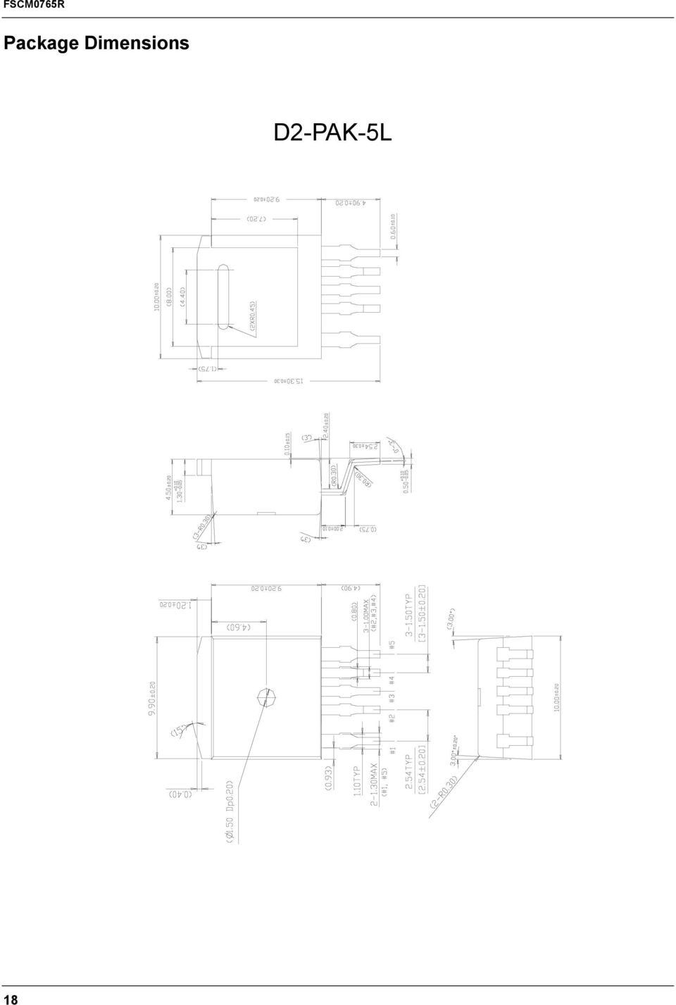
18 Package Dimensions D2-PAK-5L 18
19 Package Dimensions (Continued) TO-220-5L(Forming) 19

20 Ordering Information Product Number Package Marking Code BVdss Rds(on)Max. FSCM0765RD D2-PAK-5L CM0765RD 650V 1.6 Ω FSCM0765RCYDTU TO-220-5L CM0765RC 650V 1.6 Ω 20

21 DISCLAIMER FAIRCHILD SEMICONDUCTOR RESERVES THE RIGHT TO MAKE CHANGES WITHOUT FURTHER NOTICE TO ANY PRODUCTS HEREIN TO IMPROVE RELIABILITY, FUNCTION OR DESIGN. FAIRCHILD DOES NOT ASSUME ANY LIABILITY ARISING OUT OF THE APPLICATION OR USE OF ANY PRODUCT OR CIRCUIT DESCRIBED HEREIN; NEITHER DOES IT CONVEY ANY LICENSE UNDER ITS PATENT RIGHTS, NOR THE RIGHTS OF OTHERS. LIFE SUPPORT POLICY FAIRCHILD S PRODUCTS ARE NOT AUTHORIZED FOR USE AS CRITICAL COMPONENTS IN LIFE SUPPORT DEVICES OR SYSTEMS WITHOUT THE EXPRESS WRITTEN APPROVAL OF THE PRESIDENT OF FAIRCHILD SEMICONDUCTOR CORPORATION. As used herein: 1. Life support devices or systems are devices or systems which, (a) are intended for surgical implant into the body, or (b) support or sustain life, and (c) whose failure to perform when properly used in accordance with instructions for use provided in the labeling, can be reasonably expected to result in a significant injury of the user. 2. A critical component in any component of a life support device or system whose failure to perform can be reasonably expected to cause the failure of the life support device or system, or to affect its safety or effectiveness. 10/18/04 0.0m Fairchild Semiconductor Corporation
SD4840/4841/4842/4843/4844
 CURRENT MODE PWM CONTROLLER WITH BUILT-IN HIGH VOLTAGE MOSFET DESCRIPTION SD4840/4841/4842/4843/4844 is a current mode PWM controller with low standby power and low start current for power switch. In standby
FSDH0265RN, FSDM0265RN
 Green Mode Fairchild Power Switch (FPS TM ) www.fairchildsemi.com Features Internal Avalanche Rugged Sense FET Consumes only 0.65W at 240VAC & 0.3W load with Advanced Burst-Mode Operation Frequency Modulation
FSL128MRT Green-Mode Fairchild Power Switch (FPS ) for High Input Voltage
 for High Input Voltage") FSL128MRT Green-Mode Fairchild Power Switch (FPS ) for High Input Voltage Features Internal Avalanched Rugged 800V SenseFET Advanced Soft Burst-Mode Operation for Low Standby Power and Low audible noise
FSL128MRT Green-Mode Fairchild Power Switch (FPS ) for High Input Voltage Features Internal Avalanched Rugged 800V SenseFET Advanced Soft Burst-Mode Operation for Low Standby Power and Low audible noise
UC3842/UC3843/UC3844/UC3845
 SMPS Controller www.fairchildsemi.com Features Low Start up Current Maximum Duty Clamp UVLO With Hysteresis Operating Frequency up to 500KHz Description The UC3842/UC3843/UC3844/UC3845 are fixed frequencycurrent-mode
UNISONIC TECHNOLOGIES CO., LTD
 UPS61 UNISONIC TECHNOLOGIES CO., LTD HIGH PERFORMANCE CURRENT MODE POWER SWITCH DESCRIPTION The UTC UPS61 is designed to provide several special enhancements to satisfy the needs, for example, Power-Saving
KA7500C. SMPS Controller. Features. Description. Internal Block Diagram. www.fairchildsemi.com
 SMPS Controller www.fairchildsemi.com Features Internal Regulator Provides a Stable 5V Reference Supply Trimmed to ±1% Accuracy. Uncommitted Output TR for 200mA Sink or Source Current Output Control for
N-channel enhancement mode TrenchMOS transistor
 FEATURES SYMBOL QUICK REFERENCE DATA Trench technology d V DSS = V Low on-state resistance Fast switching I D = A High thermal cycling performance Low thermal resistance R DS(ON) mω (V GS = V) g s R DS(ON)
IRF150 [REF:MIL-PRF-19500/543] 100V, N-CHANNEL. Absolute Maximum Ratings
![IRF150 [REF:MIL-PRF-19500/543] 100V, N-CHANNEL. Absolute Maximum Ratings](/thumbs/40/21333646.jpg "IRF150 [REF:MIL-PRF-19500/543] 100V, N-CHANNEL. Absolute Maximum Ratings") PD - 90337G REPETITIVE AVALANCHE AND dv/dt RATED HEXFET TRANSISTORS THRU-HOLE (TO-204AA/AE) Product Summary Part Number BVDSS RDS(on) ID IRF150 100V 0.055Ω 38A IRF150 JANTX2N6764 JANTXV2N6764 [REF:MIL-PRF-19500/543]
PD - 90337G REPETITIVE AVALANCHE AND dv/dt RATED HEXFET TRANSISTORS THRU-HOLE (TO-204AA/AE) Product Summary Part Number BVDSS RDS(on) ID IRF150 100V 0.055Ω 38A IRF150 JANTX2N6764 JANTXV2N6764 [REF:MIL-PRF-19500/543]
Switching Regulators. STR-A6169 Universal-Input/5 W Flyback Switching Regulator FUNCTIONAL BLOCK DIAGRAM
 ABSOLUTE MAXIMUM RATINGS at T A = +25 C Control Supply Voltage, V CC.... 35 V Drain-Source Voltage, V DSS...... 800 V Drain Switching Current, I D.... 1.2 A* Peak Drain Switching Current, I DM.................................
LD7550-B. Green-Mode PWM Controller. General Description. Features. Applications. Typical Application. REV: 01a 12/22/2006 LD7550-B
 12/22/2006 REV: 01a Green-Mode PWM Controller General Description The LD7550-B is a low cost, low startup current, current mode PWM controller with green-mode power-saving operation. The integrated functions
LDS8720. 184 WLED Matrix Driver with Boost Converter FEATURES APPLICATION DESCRIPTION TYPICAL APPLICATION CIRCUIT
 184 WLED Matrix Driver with Boost Converter FEATURES High efficiency boost converter with the input voltage range from 2.7 to 5.5 V No external Schottky Required (Internal synchronous rectifier) 250 mv
LM2704 Micropower Step-up DC/DC Converter with 550mA Peak Current Limit
 Micropower Step-up DC/DC Converter with 550mA Peak Current Limit General Description The LM2704 is a micropower step-up DC/DC in a small 5-lead SOT-23 package. A current limited, fixed off-time control
AND8480/D. CrM Buck LED Driver Evaluation Board APPLICATION NOTE
 CrM Buck LED Driver Evaluation Board Prepared by: Fabien Franc ON Semiconductor Introduction This document describes the CrM Buck LED driver evaluation board. This board provides a step down converter
Symbol Parameter Value Unit IAR Avalanche Current, Repetitive or Not-Repetitive
 BUZ11 N - CHANNEL 50V - 0.03Ω - 30A -TO-220 STripFET POWER MOSFET TYPE V DSS R DS(on) I D BUZ11 50 V < 0.04 Ω 30 A TYPICAL R DS(on) = 0.03 Ω AVALANCHE RUGGED TECHNOLOGY 100% AVALANCHE TESTED HIGH CURRENT
STP6N60FI N - CHANNEL ENHANCEMENT MODE POWER MOS TRANSISTOR
 N - CHANNEL ENHANCEMENT MODE POWER MOS TRANSISTOR TYPE VDSS RDS(on) ID STP6N60FI 600 V < 1.2 Ω 3.8 A TYPICAL R DS(on) =1Ω AVALANCHE RUGGED TECHNOLOGY 100% AVALANCHE TESTED REPETITIVE AVALANCHE DATA AT
IRLR8743PbF IRLU8743PbF HEXFET Power MOSFET
 Applications l High Frequency Synchronous Buck Converters for Computer Processor Power l High Frequency Isolated DC-DC Converters with Synchronous Rectification for Telecom and Industrial Use l Lead-Free
FAN5346 Series Boost LED Driver with PWM Dimming Interface
 FAN5346 Series Boost LED Driver with PWM Dimming Interface Features Asynchronous Boost Converter Drives LEDs in Series: FAN5346S20X: 20V Output FAN5346S30X: 30V Output 2.5V to 5.5V Input Voltage Range
MP2259 1A, 16V, 1.4MHz Step-Down Converter
 MP59 1A, 1V, 1.MHz Step-Down Converter TM The Future of Analog IC Technology DESCRIPTION The MP59 is a monolithic integrated stepdown switch mode converter with an internal power MOSFET. It achieves 1A
BUZ11. 30A, 50V, 0.040 Ohm, N-Channel Power MOSFET. Features. [ /Title (BUZ1 1) /Subject. (30A, 50V, 0.040 Ohm, N- Channel. Ordering Information
 /Subject. (30A, 50V, 0.040 Ohm, N- Channel. Ordering Information") Data Sheet June 1999 File Number 2253.2 [ /Title (BUZ1 1) /Subject (3A, 5V,.4 Ohm, N- Channel Power MOS- FET) /Autho r () /Keywords (Intersil Corporation, N- Channel Power MOS- FET, TO- 22AB ) /Creator
Data Sheet June 1999 File Number 2253.2 [ /Title (BUZ1 1) /Subject (3A, 5V,.4 Ohm, N- Channel Power MOS- FET) /Autho r () /Keywords (Intersil Corporation, N- Channel Power MOS- FET, TO- 22AB ) /Creator
400KHz 60V 4A Switching Current Boost / Buck-Boost / Inverting DC/DC Converter
 Features Wide 5V to 32V Input Voltage Range Positive or Negative Output Voltage Programming with a Single Feedback Pin Current Mode Control Provides Excellent Transient Response 1.25V reference adjustable
Constant Voltage and Constant Current Controller for Adaptors and Battery Chargers
 TECHNICAL DATA Constant Voltage and Constant Current Controller for Adaptors and Battery Chargers IK3051 Description IK3051 is a highly integrated solution for SMPS applications requiring constant voltage
200V, N-CHANNEL. Absolute Maximum Ratings. Features: www.irf.com 1 PD - 90370
 PD - 90370 REPETITIVE AVALANCHE AND dv/dt RATED HEXFET TRANSISTORS THRU-HOLE (TO-204AA/AE) IRF240 200V, N-CHANNEL Product Summary Part Number BVDSS RDS(on) ID IRF240 200V 0.18Ω 18A The HEXFET technology
Preliminary Datasheet
 Features Macroblock Preliminary Datasheet 1.2A Constant Output Current 93% Efficiency @ input voltage 13V, 350mA, 9~36V Input Voltage Range Hysteretic PFM Improves Efficiency at Light Loads Settable Output
Push-Pull FET Driver with Integrated Oscillator and Clock Output
 19-3662; Rev 1; 5/7 Push-Pull FET Driver with Integrated Oscillator General Description The is a +4.5V to +15V push-pull, current-fed topology driver subsystem with an integrated oscillator for use in
TDA4605 CONTROL CIRCUIT FOR SWITCH MODE POWER SUPPLIES USING MOS TRANSISTORS
 CONTROL CIRCUIT FOR SWITCH MODE POWER SUPPLIES USING MOS TRANSISTORS Fold-Back Characteristic provides Overload Protection for External Diodes Burst Operation under Short-Circuit and no Load Conditions
High Performance Current Mode PWM Controller Cycle Turning + POWER FROM LIEMIC. For, 2008 LIEMIC Semiconductor Co.,Ltd. LN3C63AD REV: 1.0.
 LN3C63 High Performance Current Mode PWM Controller Cycle Turning + POWER FROM LIEMIC For, Adaptor & Charger Offline Power Supply Open Frame Power DVD&DVB Player Auxiliary Power for PC etc..... 2008 LIEMIC
UNISONIC TECHNOLOGIES CO., LTD UC3863 LINEAR INTEGRATED CIRCUIT
 UNISONIC TECHNOLOGIES CO., LTD UC3863 LOW COST POWER-SAVING MODE PWM CONTROLLER FOR FLYBACK CONVERTERS DESCRIPTION The UC3863 is a high performance current mode PWM controller ideally suited for low standby
AP1509. 150KHz, 2A PWM BUCK DC/DC CONVERTER. Description. Pin Assignments V IN. Applications. Features. (Top View) GND GND. Output AP1509 GND GND
 GND GND. Output AP1509 GND GND") Description Pin Assignments The series are monolithic IC designed for a stepdown DC/DC converter, and own the ability of driving a 2A load without additional transistor. It saves board space. The external
Description Pin Assignments The series are monolithic IC designed for a stepdown DC/DC converter, and own the ability of driving a 2A load without additional transistor. It saves board space. The external
5A 3A. Symbol Parameter Value Unit
 STP5NA50 STP5NA50FI N - CHANNEL ENHANCEMENT MODE FAST POWER MOS TRANSISTOR TYPE VDSS RDS(on) ID STP5NA50 STP5NA50FI 500 V 500 V
PAM2804. Pin Assignments. Description. Applications. Features. Typical Applications Circuit 1A STEP-DOWN CONSTANT CURRENT, HIGH EFFICIENCY LED DRIVER
 1A STEP-DOWN CONSTANT CURRENT, HIGH EFFICIENCY LED DRIER Description Pin Assignments The is a step-down constant current LED driver. When the input voltage is down to lower than LED forward voltage, then
Power Management & Supply. Design Note. Version 1.0, Nov. 2001 DN-EVALMF2ICE2A265-1. CoolSET 35W DVD Power Supply with ICE2A265.
 Version 1.0, Nov. 2001 Design Note DN-EVALMF2ICE2A265-1 CoolSET 35W DVD Power Supply with ICE2A265 Author: Harald Zöllinger Published by Infineon Technologies AG http://www.infineon.com Power Management
SG2525A SG3525A REGULATING PULSE WIDTH MODULATORS
 SG2525A SG3525A REGULATING PULSE WIDTH MODULATORS 8 TO 35 V OPERATION 5.1 V REFERENCE TRIMMED TO ± 1 % 100 Hz TO 500 KHz OSCILLATOR RANGE SEPARATE OSCILLATOR SYNC TERMINAL ADJUSTABLE DEADTIME CONTROL INTERNAL
Datasheet. 2A 380KHZ 20V PWM Buck DC/DC Converter. Features
 General Description Features The is a 380 KHz fixed frequency monolithic step down switch mode regulator with a built in internal Power MOSFET. It achieves 2A continuous output current over a wide input
AP1506. 150KHz, 3A PWM BUCK DC/DC CONVERTER. Pin Assignments. Description. Features. Applications. ( Top View ) 5 SD 4 FB 3 Gnd 2 Output 1 V IN
 5 SD 4 FB 3 Gnd 2 Output 1 V IN") Description Pin Assignments The series are monolithic IC designed for a stepdown DC/DC converter, and own the ability of driving a 3A load without external transistor. Due to reducing the number of external
Description Pin Assignments The series are monolithic IC designed for a stepdown DC/DC converter, and own the ability of driving a 3A load without external transistor. Due to reducing the number of external
AN-8019 Reliable USB Modem Design Using the Combination of an Integrated Load Switch and a Buck Converter
 www.fairchildsemi.com AN-8019 Reliable USB Modem Design Using the Combination of an Integrated Load Switch and a Buck Converter Introduction In the portable electronics market, a wireless network allows
LM5001 High Voltage Switch Mode Regulator
 High Voltage Switch Mode Regulator General Description The LM5001 high voltage switch mode regulator features all of the functions necessary to implement efficient high voltage Boost, Flyback, SEPIC and
CE8301 Series. Introduction. Features. Ordering Information. Applications SMALL PACKAGE PFM CONTROL STEP-UP DC/DC CONVERTER
 SMALL PACKAGE PFM CONTROL STEP-UP DC/DC CONVERTER Introduction The is a CMOS PFM-control step-up switching DC/DC converter that mainly consists of a reference voltage source, an oscillator, and a comparator.
FEBFL7701_L30U003A. 2.4W LED Ballast Using FL7701. Featured Fairchild Product: FL7701
 User Guide for FEBFL7701_L30U003A 2.4W LED Ballast Using FL7701 Featured Fairchild Product: FL7701 Direct questions or comments about this evaluation board to: Worldwide Direct Support Fairchild Semiconductor.com
28V, 2A Buck Constant Current Switching Regulator for White LED
 28V, 2A Buck Constant Current Switching Regulator for White LED FP7102 General Description The FP7102 is a PWM control buck converter designed to provide a simple, high efficiency solution for driving
AC/DC Power Management Devices. 2015 Product Guide. AC/DC Control ICs with integrated MOSFETs in LLC, QR & PWM Topologies
 AC/DC Power Management Devices 2015 Product Guide AC/DC Control ICs with integrated MOSFETs in LLC, QR & PWM Topologies About Us Headquarters Japan Sanken Electric Co., Ltd. is a Japanese company who s
Features. Symbol JEDEC TO-220AB
 Data Sheet June 1999 File Number 2253.2 3A, 5V,.4 Ohm, N-Channel Power MOSFET This is an N-Channel enhancement mode silicon gate power field effect transistor designed for applications such as switching
PHOTOTRANSISTOR OPTOCOUPLERS
 MCT2 MCT2E MCT20 MCT27 WHITE PACKAGE (-M SUFFIX) BLACK PACKAGE (NO -M SUFFIX) DESCRIPTION The MCT2XXX series optoisolators consist of a gallium arsenide infrared emitting diode driving a silicon phototransistor
Theory of Operation. Figure 1 illustrates a fan motor circuit used in an automobile application. The TPIC2101. 27.4 kω AREF.
 In many applications, a key design goal is to minimize variations in power delivered to a load as the supply voltage varies. This application brief describes a simple DC brush motor control circuit using
How To Make A Field Effect Transistor (Field Effect Transistor) From Silicon P Channel (Mos) To P Channel Power (Mos) (M2) (Mm2)
 From Silicon P Channel (Mos) To P Channel Power (Mos) (M2) (Mm2)") TPC811 TOSHIBA Field Effect Transistor Silicon P Channel MOS Type (U-MOS III) TPC811 Lithium Ion Battery Applications Notebook PC Applications Portable Equipment Applications Unit: mm Small footprint due
TPC811 TOSHIBA Field Effect Transistor Silicon P Channel MOS Type (U-MOS III) TPC811 Lithium Ion Battery Applications Notebook PC Applications Portable Equipment Applications Unit: mm Small footprint due
FAN8082 (KA3082N) Bi-directional DC Motor Driver. Features. Description. Typical Applications. Ordering Information. www.fairchildsemi.
 Bi-directional DC Motor Driver. Features. Description. Typical Applications. Ordering Information. www.fairchildsemi.") Bi-directional DC Motor Driver www.fairchildsemi.com Features Built-in brake function for stable brake characteristics. Built-in element to absorb a surge current derived from changing motor direction
Bi-directional DC Motor Driver www.fairchildsemi.com Features Built-in brake function for stable brake characteristics. Built-in element to absorb a surge current derived from changing motor direction
LM741. Single Operational Amplifier. Features. Description. Internal Block Diagram. www.fairchildsemi.com
 Single Operational Amplifier www.fairchildsemi.com Features Short circuit protection Excellent temperature stability Internal frequency compensation High Input voltage range Null of offset Description
Features. Description. Table 1. Device summary. Order code Marking Package Packing. STP110N8F6 110N8F6 TO-220 Tube
 N-channel 80 V, 0.0056 Ω typ.,110 A, STripFET F6 Power MOSFET in a TO-220 package Features Datasheet - production data Order code V DS R DS(on)max I D P TOT TAB STP110N8F6 80 V 0.0065 Ω 110 A 200 W TO-220
FAN7680. PC Power Supply Outputs Monitoring IC. Features. Description. Typical Application. www.fairchildsemi.com FPO OVP UVP PGO PSON
 PC Power Supply Outputs Monitoring IC www.fairchildsemi.com Features PC Power Supply Output Monitor Circuitry Few External Components Over Voltage Protection for.v, V and V(Vcc) Outputs Under Voltage Protection
Application Note AN4137
 www.fairchildsemi.com Application Note AN4137 Design Guidelines for Offline Flyback Converters Using Fairchild Power Switch (FPS) Abstract This paper presents practical design guidelines for offline flyback
29V High Voltage LED Driver
 29V High Voltage LED Driver SP7601 FEATURES Wide Input Voltage Range 4.5V 29V 1.2MHz Constant Frequency Operation Low 0.2V Reference Voltage Adjustable Overcurrent Protection PWM Dimming and Power sequencing
IR1168S DUAL SMART RECTIFIER DRIVER IC
 Datasheet No PD97382 September 26, 2011 IR1168S DUAL SMART RECTIFIER DRIVER IC Features Secondary-side high speed controller for synchronous rectification in resonant half bridge topologies 200V proprietary
IRF830. N - CHANNEL 500V - 1.35Ω - 4.5A - TO-220 PowerMESH MOSFET
 IRF830 N - CHANNEL 500V - 1.35Ω - 4.5A - TO-220 PowerMESH MOSFET TYPE V DSS R DS(on) I D IRF830 500 V < 1.5 Ω 4.5 A TYPICAL R DS(on) = 1.35 Ω EXTREMELY HIGH dv/dt CAPABILITY 100% AVALANCHE TESTED VERY
MC33064DM 5 UNDERVOLTAGE SENSING CIRCUIT
 Order this document by MC3464/D The MC3464 is an undervoltage sensing circuit specifically designed for use as a reset controller in microprocessor-based systems. It offers the designer an economical solution
STW20NM50 N-CHANNEL 550V @ Tjmax - 0.20Ω - 20ATO-247 MDmesh MOSFET
 N-CHANNEL 550V @ Tjmax - 0.20Ω - 20ATO-247 MDmesh MOSFET TYPE V DSS (@Tjmax) R DS(on) I D STW20NM50 550V < 0.25Ω 20 A TYPICAL R DS (on) = 0.20Ω HIGH dv/dt AND AVALANCHE CAPABILITIES 100% AVALANCHE TESTED
FPAB20BH60B PFC SPM 3 Series for Single-Phase Boost PFC
 FPAB20BH60B PFC SPM 3 Series for Single-Phase Boost PFC Features UL Certified No. E209204 (UL1557) 600 V - 20 A Single-Phase Boost PFC with Integral Gate Driver and Protection Very Low Thermal Resistance
HIGH SPEED-10 MBit/s LOGIC GATE OPTOCOUPLERS
 DESCRIPTION The, /6 single-channel and /6 dual-channel optocouplers consist of a 5 nm AlGaAS LED, optically coupled to a very high speed integrated photodetector logic gate with a strobable output. This
How To Make A Power Supply For A Flyback Power Supply
 Design Note DN0501/D A 0 to 5 Watt, Low Cost, Off-line Power Supply Device Application Input Voltage Output Power Topology I/O Isolation White Goods, Small NCP151B Instruments, E- NCP41 90 67 Vac 0 to
TOSHIBA Insulated Gate Bipolar Transistor Silicon N Channel IGBT GT60J323
 GT6J2 TOSHIBA Insulated Gate Bipolar Transistor Silicon N Channel IGBT GT6J2 Current Resonance Inverter Switching Application Unit: mm Enhancement mode type High speed : t f =.6 μs (typ.) (I C = 6A) Low
LM2576R. 3.0A, 52kHz, Step-Down Switching Regulator FEATURES. Applications DESCRIPTION TO-220 PKG TO-220V PKG TO-263 PKG ORDERING INFORMATION
 LM2576 FEATURES 3.3, 5.0, 12, 15, and Adjustable Output ersions Adjustable ersion Output oltage Range, 1.23 to 37 +/- 4% AG10Maximum Over Line and Load Conditions Guaranteed 3.0A Output Current Wide Input
Low power offline switched-mode power supply primary switcher. 60kHz OSCILLATOR PWM LATCH Q R4 S FF R3 R1 R2 + BLANKING + OVERVOLTAGE LATCH
 Low power offline switched-mode power supply primary switcher Features Fixed 60 khz switching frequency 9 V to 38 V wide range V DD voltage Current mode control Auxiliary undervoltage lockout with hysteresis
Features 1.7 A, 20 V. R DS(ON) Symbol Parameter Ratings Units
 Symbol Parameter Ratings Units") N-Channel.5V Specified PowerTrench TM MOSFET April 999 General Description This N-Channel.5V specified MOSFET is produced using Fairchild Semiconductor's advanced PowerTrench process that has been especially
N-Channel.5V Specified PowerTrench TM MOSFET April 999 General Description This N-Channel.5V specified MOSFET is produced using Fairchild Semiconductor's advanced PowerTrench process that has been especially
Series AMLDL-Z Up to 1000mA LED Driver
 FEATURES: Click on Series name for product info on aimtec.com Series Up to ma LED Driver Models Single output Model Input Voltage (V) Step Down DC/DC LED driver Operating Temperature range 4ºC to 85ºC
Features. T A=25 o C unless otherwise noted. Symbol Parameter Ratings Units. (Note 1b) 0.46
 0.46") N-Channel.8 Vgs Specified PowerTrench MOSFET October 2 General Description This 2V N-Channel MOSFET uses Fairchild s high voltage PowerTrench process. It has been optimized for power management applications.
N-Channel.8 Vgs Specified PowerTrench MOSFET October 2 General Description This 2V N-Channel MOSFET uses Fairchild s high voltage PowerTrench process. It has been optimized for power management applications.
MP1541 1.3MHz Boost Converter
 MP5.3MHz Boost Converter The Future of Analog IC Technology DESCRIPTION The MP5 is a 5-pin thin SOT3 current mode step up converter intended for small, low power applications. The MP5 switches at.3mhz
AP1510. General Description. Features. Applications. Typical Application Circuit PWM CONTROL 3A STEP-DOWN CONVERTER AP1510. x (1+R A = V FB /R B
 Features General Description Input voltage: 3.6 to 23 Output voltage: 0.8 to CC. Duty ratio: 0% to 100% PWM control Oscillation frequency: 300kHz typ. Current Limit, Enable function Thermal Shutdown function
VIPer22A-E VIPer22ADIP-E, VIPer22AS-E
 VIPer22A-E VIPer22ADIP-E, VIPer22AS-E Low power OFF-line SMPS primary switcher Features Fixed 60 khz switching frequency 9 V to 38 V wide range V DD voltage Current mode control Auxiliary undervoltage
FEATURES DESCRIPTION APPLICATIONS BLOCK DIAGRAM. PT2248 Infrared Remote Control Transmitter
 Infrared Remote Control Transmitter DESCRIPTION PT2248 is an infrared remote control transmitter utilizing CMOS Technology. It is capable of 18 functions and a total of 75 commands. Single-shot and continuous
IS32BL3554 BOOST TYPE LED DRIVER WITH 4-CHANNEL CURRENT SOURCE
 ISBL BOOST TYPE LED DRIVER WITH -CHANNEL CURRENT SOURCE DESCRIPTION The ISBL is a white LED driver for backlight applications based on a highly efficient boost controller operating over a wide input voltage
WHITE LED STEP-UP CONVERTER. Features
 General Description The is an inductor-based DC/DC converter designed to drive up to eight white LEDs in series for backlight. Only one feedback resistor is needed to control the LED current and obtain
unit : mm With heat sink (see Pd Ta characteristics)
") Ordering number: EN1321E Monolithic Linear IC LA4261 3.5 W 2-Channel AF Power Amplifier for Home Stereos and Music Centers Features. Minimum number of external parts required (No input capacitor, bootstrap
Ordering number: EN1321E Monolithic Linear IC LA4261 3.5 W 2-Channel AF Power Amplifier for Home Stereos and Music Centers Features. Minimum number of external parts required (No input capacitor, bootstrap
IRLR8729PbF IRLU8729PbF
 Applications l High Frequency Synchronous Buck Converters for Computer Processor Power l High Frequency Isolated DC-DC Converters with Synchronous Rectification for Telecom and Industrial Use Benefits
Programmable Single-/Dual-/Triple- Tone Gong SAE 800
 Programmable Single-/Dual-/Triple- Tone Gong Preliminary Data SAE 800 Bipolar IC Features Supply voltage range 2.8 V to 18 V Few external components (no electrolytic capacitor) 1 tone, 2 tones, 3 tones
AC/DC Power Supply Reference Design. Advanced SMPS Applications using the dspic DSC SMPS Family
 AC/DC Power Supply Reference Design Advanced SMPS Applications using the dspic DSC SMPS Family dspic30f SMPS Family Excellent for Digital Power Conversion Internal hi-res PWM Internal high speed ADC Internal
1.5A ASYNCHRONOUS DC-DC BUCK CONV
 General Description The is a 1.4MHz fixed frequency, current mode, PWM buck (step-down) DC-DC converter, capable of driving a 1.5A load with high efficiency, excellent line and load regulation. The device
EST7502B PC Power Supply PWM with Supervisor
 GENERAL DESCRIPTION The EST7502B is a pulse width modulation (PWM) control circuit with complete protection circuits for used in the SMPS (Switched Mode Power Supply). It contains various functions, which
AN2228 APPLICATION NOTE
 AN2228 APPLICATION NOTE STD1LNK60Z-based Cell Phone Battery Charger Design Introduction This application note is a Ringing Choke Converter (RCC)-based, step-by-step cell phone battery charger design procedure.
STCS1A. 1.5 A max constant current LED driver. Features. Applications. Description
 1.5 A max constant current LED driver Features Up to 40 V input voltage Less than 0.5 V voltage overhead Up to 1.5 A output current PWM dimming pin Shutdown pin LED disconnection diagnostic DFN8 (3 x 3
MM74HC4538 Dual Retriggerable Monostable Multivibrator
 MM74HC4538 Dual Retriggerable Monostable Multivibrator General Description The MM74HC4538 high speed monostable multivibrator (one shots) is implemented in advanced silicon-gate CMOS technology. They feature
NCT3941S/S-A Nuvoton 4 Times Linear Fan Driver NCT3941S/S-A
 Nuvoton 4 Times Linear Fan Driver NCT3941S/S-A -I- Revision A4 Table of Content- 1. GENERAL DESCRIPTION...1 2. FEATURES...1 3. APPLICATION...1 4. BLOCK DIAGRAM...2 5. PIN CONFIGURATION AND TYPICAL APPLICATION
HV start-up DCM/QR flyback controller with integrated DCM/QR PFC controller
 HV start-up DCM/QR flyback with integrated DCM/QR PFC Rev. 1.1 13 March 2015 Product data sheet 1. General description The GreenChip is the latest generation of green Switched Mode Power Supply (SMPS)
CAT4101TV. 1 A Constant-Current LED Driver with PWM Dimming
 A Constant-Current LED Driver with PWM Dimming Description The CAT4 is a constant current sink driving a string of high brightness LEDs up to A with very low dropout of.5 V at full load. It requires no
STOD2540. PMOLED display power supply. Features. Application. Description
 PMOLED display power supply Features Inductor switches boost controller PFM mode control High efficiency over wide range of load (1 ma to 40 ma) Integrated load disconnect switch Over voltage protection
STP10NK80ZFP STP10NK80Z - STW10NK80Z
 STP10NK80ZFP STP10NK80Z - STW10NK80Z N-channel 800V - 0.78Ω - 9A - TO-220/FP-TO-247 Zener-protected supermesh TM MOSFET General features Type V DSS R DS(on) I D Pw STP10NK80Z 800V
Pulse Width Modulation Amplifiers EQUIVALENT CIRCUIT DIAGRAM. 200mV + - SMART CONTROLLER .01F OSC Q3. 2200pF
 Pulse Width Modulation Amplifiers MSA MSA FEATURES LOW COST HIGH VOLTAGE VOLTS HIGH OUTPUT CURRENT AMPS kw OUTPUT CAPABILITY VARIABLE SWITCHING FREQUEY APPLICATIONS BRUSH MOTOR CONTROL MRI MAGNETIC BEARINGS
Enpirion Power Datasheet EP53F8QI 1500 ma PowerSoC Voltage Mode Synchronous PWM Buck with Integrated Inductor
 Enpirion Power Datasheet EP53F8QI 1500 ma PowerSoC Voltage Mode Synchronous PWM Buck with Integrated Inductor Description The EP53F8QI provides high efficiency in a very small footprint. Featuring integrated
TSM2N7002K 60V N-Channel MOSFET
 SOT-23 SOT-323 Pin Definition: 1. Gate 2. Source 3. Drain PRODUCT SUMMARY V DS (V) R DS(on) (Ω) I D (ma) 5 @ V GS = 10V 100 60 5.5 @ V GS = 5V 100 Features Low On-Resistance ESD Protection High Speed Switching
MM74HC14 Hex Inverting Schmitt Trigger
 MM74HC14 Hex Inverting Schmitt Trigger General Description The MM74HC14 utilizes advanced silicon-gate CMOS technology to achieve the low power dissipation and high noise immunity of standard CMOS, as
AP3125A/V/L/R. Description. Pin Assignments NEW PRODUCT. Features. Applications. A Product Line of. Diodes Incorporated GREEN MODE PWM CONTROLLER
 Description Pin Assignments GREEN MODE PWM CONTROLLER The is a current mode PWM controller which is optimized for high performance, low standby power and cost effective offline flyback converters. (Top
IS31LT3360 40V/1.2A LED DRIVER WITH INTERNAL SWITCH. January 2014
 40V/1.2A LED DRIVER WITH INTERNAL SWITCH January 2014 GENERAL DESCRIPTION The IS31LT3360 is a continuous mode inductive step-down converter, designed for driving a single LED or multiple series connected
FDD4243 40V P-Channel PowerTrench MOSFET -40V, -14A, 44mΩ Features
 FDD443 4V P-Channel PowerTrench MOSFET -4V, -4A, 44mΩ Features Max r DS(on) = 44mΩ at V GS = -V, I D = -6.7A Max r DS(on) = 64mΩ at V GS = -4.5V, I D = -5.5A High performance trench technology for extremely
IPS511/IPS511S FULLY PROTECTED HIGH SIDE POWER MOSFET SWITCH. Load
 Data Sheet No.PD 6155 IPS511/IPS511S FUY PROTECTED IG SIDE POWER MOSFET SWITC Features Over temperature protection (with auto-restart) Short-circuit protection (current limit ) Active clamp E.S.D protection
LB1836M. Specifications. Monolithic Digital IC Low-Saturation Bidirectional Motor Driver for Low-Voltage Drive. Absolute Maximum Ratings at Ta = 25 C
 Ordering number : EN397F LB136M Monolithic Digital IC Low-Saturation Bidirectional Motor Driver for Low-Voltage Drive http://onsemi.com Overview The LB136M is a low-saturation two-channel bidirectional
MIC33050. General Description. Features. Applications. Typical Application. 4MHz Internal Inductor PWM Buck Regulator with HyperLight Load
 4MHz Internal Inductor PWM Buck Regulator with HyperLight Load General Description The Micrel is a high-efficiency 600mA PWM synchronous buck (step-down) regulator with internal inductor featuring HyperLight
LM555/NE555/SA555. Single Timer. Description. Features. Applications. Internal Block Diagram. Vcc GND. Trigger. Discharge. Output F/F.
 Single Timer www.fairchildsemi.com Features High Current Drive Capability (00mA) Adjustable Duty Cycle Temperature Stability of 0.005%/ C Timing From µsec to Hours Turn off Time Less Than µsec Applications
IRFP450. N - CHANNEL 500V - 0.33Ω - 14A - TO-247 PowerMESH MOSFET
 IRFP450 N - CHANNEL 500V - 0.33Ω - 14A - TO-247 PowerMESH MOSFET TYPE V DSS R DS(on) I D IRFP450 500 V < 0.4 Ω 14 A TYPICAL R DS(on) = 0.33 Ω EXTREMELY HIGH dv/dt CAPABILITY 100% AVALANCHE TESTED VERY
SPI-8001TW. Switching Regulators. Dual 1.5 A, DC/DC Step-Down Converter. SANKEN ELECTRIC CO., LTD. http://www.sanken-ele.co.jp/en/
 Data Sheet 27469.301.1 Designed to meet high-current requirements at high efficiency in industrial and consumer applications; embedded core, memory, or logic supplies; TVs, VCRs, and office equipment,
STCS2A. 2 A max constant current LED driver. Features. Applications. Description
 2 A max constant current LED driver Features Up to 40 V input voltage Less than 0.5 V voltage overhead Up to 2 A output current PWM dimming pin Shutdown pin LED disconnection diagnostic Slope control with
µpfc ONE CYCLE CONTROL PFC IC
 Features PFC with IR proprietary One Cycle Control Continuous conduction mode (CCM) boost type PFC No line voltage sense required Programmable switching frequency (50kHz-200kHz) Programmable output overvoltage
IRF740 N-CHANNEL 400V - 0.46Ω - 10A TO-220 PowerMESH II MOSFET
 N-CHANNEL 400V - 0.46Ω - 10A TO-220 PowerMESH II MOSFET TYPE V DSS R DS(on) I D IRF740 400 V < 0.55 Ω 10 A TYPICAL R DS (on) = 0.46Ω EXCEPTIONAL dv/dt CAPABILITY 100% AVALANCHE TESTED LOW GATE CHARGE VERY
LM139/LM239/LM339/LM2901/LM3302 Low Power Low Offset Voltage Quad Comparators
 Low Power Low Offset Voltage Quad Comparators General Description The LM139 series consists of four independent precision voltage comparators with an offset voltage specification as low as 2 mv max for