Constant Voltage and Constant Current Controller for Adaptors and Battery Chargers
|
|
|
- Marianna Morris
- 9 years ago
- Views:
Transcription
1 TECHNICAL DATA Constant Voltage and Constant Current Controller for Adaptors and Battery Chargers IK3051 Description IK3051 is a highly integrated solution for SMPS applications requiring constant voltage and constant current mode. IK3051 integrates one voltage reference, two operational amplifiers (with ORed outputs common collectors), and a current sensing circuit. The voltage reference combined with one operational amplifier makes it an ideal voltage controller, and the other low voltage reference combined with the other operational amplifier makes it an ideal current limiter for output low side current sensing. The current threshold is fixed and precise. The only external components are: A resistor bridge to be connected to the output of the power supply (adapter, battery charger) to set the voltage regulation by dividing the desired output voltage to match the internal voltage reference value. A sense resistor having a value and allowable dissipation power which need to be chosen according to the internal voltage threshold. Optional compensation components (R and C). IK3051, is ideal for smallest package available, is ideal for space shrinked applications such as adapters and battery chargers. PIN CONNECTION (top view) Features CONSTANT VOLTAGE AND CONSTANT CURRENT CONTROL LOW VOLTAGE OPERATION PRECISION INTERNAL COMPONENT COUNT CURRENT SINK OUTPUT STAGE EASY COMPENSATION LOW AC MAINS VOLTAGE REJECTION ORDERING INFORMATION Device IK3051S2T Operating Temperature Range T A = 0 to 85 C for all packages Package Plastic SOT23-6 Shipping Tape& Reel Pin Definitions and Functions SOT23-6 Pin out Name Pin# Type Function Vcc 6 Power Supply Positive Power Supply Line GND 2 Power Supply Ground Line. 0V Reference For All Voltages Vctrl 1 Analog Input Input Pin of the Voltage Control Loop Ictrl 4 Analog Input Input Pin of the Current Control Loop Out 3 Current Sink Output Output Pin. Sinking Current Only Vsense 5 Analog Input Input Pin of the Current Control Loop

2 Absolute Maximum Ratings Symbol Parameter Value Unit Vcc DC Supply Voltage 14 V Vi Input Voltage -0.3 to Vcc V Top Operating Free Air Temperature Range 0 to 85 o C Tj Maximum Junction Temperature 150 o C Operation Conditions Symbol Parameter Value Unit Vcc DC Supply Conditions 2.5 to 12 V Electrical Characteristics Tamb = 25 C and Vcc = +5V (unless otherwise specified) Symbol Parameter Test Condition Min Typ Max Unit Total Current Consumption Total Supply Current not taking the Tamb Icc ma output sinking current into account 1.2 Voltage Control Loop Transconduction Gain (Vctrl). Sink Tamb 3.5 Gmv Current Only 1) 1 ma/mv 2.5 2) Tamb Vref Voltage Control Loop Reference 1.21 V Tamb 50 Iibv Input Bias Current (Vctrl) na 100 Current Control Loop Transconduction Gain (Ictrl). Sink Tamb Gmi Current Only 3) 4) Iout = 2.5 ma Tamb Vsense Current Control Loop Reference Tamb Iibi Current out of pin Ictrl at -200mV Output Stage Vol Low output voltage at 10 ma sinking current Ios Output Short Circuit Current. Output to Vcc. Sink Current Only Tamb Tamb ma/mv mv µa 200 mv ma 1. If the voltage on Vctrl (the negative input of the amplifier) is higher than the positive amplifier input (Vref=1.210V), and it is increased by 1mV, the sinking current at the output OUT will be increased by 3.5mA. 2. The internal Voltage Reference is set at 1.210V (bandgap reference). The voltage control loop precision takes into account the cumulative effects of the internal voltage reference deviation as well as the input offset voltage of the trans-conductance operational amplifier. The internal Voltage Reference is fixed by bandgap, and trimmed to 1% accuracy at room temperature. 3. When the positive input at Ictrl is lower than -200mV, and the voltage is decreased by 1mV, the sinking current at the output OUT will be increased by 7mA. 4. The internal current sense threshold is set to -200mV. The current control loop precision takes into account the cumulative effects of the internal voltage reference deviation as well as the input offset voltage of the transconduction operational amplifier.
. Sink Tamb 3.5 Gmv Current Only 1) 1 ma/mv 2.5 2) Tamb 1.198 1.")
3 PRINCIPLE OF OPERATION AND APPLICATION HINTS 1. Voltage and Current Control 1.1. Voltage Control The voltage loop is controlled via a first transconductance operational amplifier, the resistor bridge R1, R2, and the optocoupler which is directly connected to the output. The relation between the values of R1 and R2 should be chosen as written in Equation 1. R1 = R2 x Vref / (Vout - Vref) Eq1 Where Vout is the desired output voltage. To avoid the discharge of the load, the resistor bridge R1, R2 should be highly resistive. For this type of application, a total value of 100KΩ (or more) would be appropriate for the resistors R1 and R2. As an example, with R2 = 100KΩ, Vout = 4.10V, Vref = 1.210V, then R1 = 41.9KΩ. Note that if the low drop diode should be inserted between the load and the voltage regulation resistor bridge to avoid current flowing from the load through the resistor bridge, this drop should be taken into account in the above calculations by replacing Vout by (Vout + Vdrop) Current Control The current loop is controlled via the second transconductance operational amplifier, the sense resistor Rsense, and the optocoupler. The control equation verifies: Rsense x Ilim = Vsense eq2 Rsense = Vsense / Ilim eq2 where Ilim is the desired limited current, and Vsense is the threshold voltage for the current control loop. As an example, with Ilim = 1A, Vsense = -200mV, then Rsense = 200mΩ. Note that the Rsense resistor should be chosen taking into account the maximum dissipation (Plim) through it during full load operation. Plim = Vsense x Ilim. eq3 As an example, with Ilim = 1A, and Vsense = 200mV, Plim = 200mW. Therefore, for most adapter and battery charger applications, a quarter-watt, or half-watt resistor to make the current sensing function is sufficient. Vsense threshold is achieved internally by a resistor bridge tied to the Vref voltage reference. Its middle point is tied to the positive input of the current control operational amplifier, and its foot is to be connected to lower potential point of the sense resistor as shown on the following figure. The resistors of this bridge are matched to provide the best precision possible. The current sinking outputs of the two transconductance operational amplifiers are common (to the output of the IC). This makes an ORing function which ensures that whenever the current or the voltage reaches too high values, the optocoupler is activated. The relation between the controlled current and the controlled output voltage can be described with a square characteristic as shown in the following V/I output-power graph. Figure 1 : Output voltage versus output current 2. Compensation The voltage-control trans-conductance operational amplifier can be fully compensated. Both of its output and negative input are directly accessible for external compensation components. An example of a suitable compensation network is shown in Fig.2. It consists of a capacitor Cvc1=2.2nF and a resistor Rcv1=470KΩ in series, connected in parallel with another capacitor Cvc2=22pF. The current-control trans-conductance operational amplifier can be fully compensated. Both of its output and negative input are directly accessible for external compensation components. An example of a suitable compensation network is shown in Fig.2. It consists of a capacitor Cic1=2.2nF and a resistor Ric1=22KΩ in series. When the Vcc voltage reaches 12V it could be interesting to limit the current coming through the output in the aim to reduce the dissipation of the device and increase the stability performances of the whole application. An example of a suitable Rout value could be 330Ω in series with the opto-coupler in case Vcc=12V. 3. Start Up and Short Circuit Conditions Under start-up or short-circuit conditions the IK3051 is not provided with a high enough supply voltage. This is due to the fact that the chip has its
 Eq1 Where Vout is the desired output voltage.")
4 power supply line in common with the power supply line of the system. Therefore, the current limitation can only be ensured by the primary PWM module, which should be chosen accordingly. If the primary current limitation is considered not to be precise enough for the application, then a sufficient supply for the IK3051 has to be ensured under any condition. It would then be necessary to add some circuitry to supply the chip with a separate power line. This can be achieved in numerous ways, including an additional winding on the transformer. The following schematic shows how to realize a low-cost power supply for the IK3051 (with no additional windings). Please pay attention to the fact that in the particular case presented here, this low-cost power supply can reach voltages as high as twice the voltage of the regulated line. Since the Absolute Maximum Rating of the IK3051 supply voltage is 14 V, this low-cost auxiliary power supply can only be used in applications where the regulated line voltage does not exceed 7 V. Figure 2 : Typical Adapter or Battery Charger Application Using IK3051 In the above application schematic, the IK3051 is used on the secondary side of a flyback adapter (or battery charger) to provide an accurate control of voltage and current. The above feedback loop is made with an optocoupler.
.")
5 Typical Application Figure 3

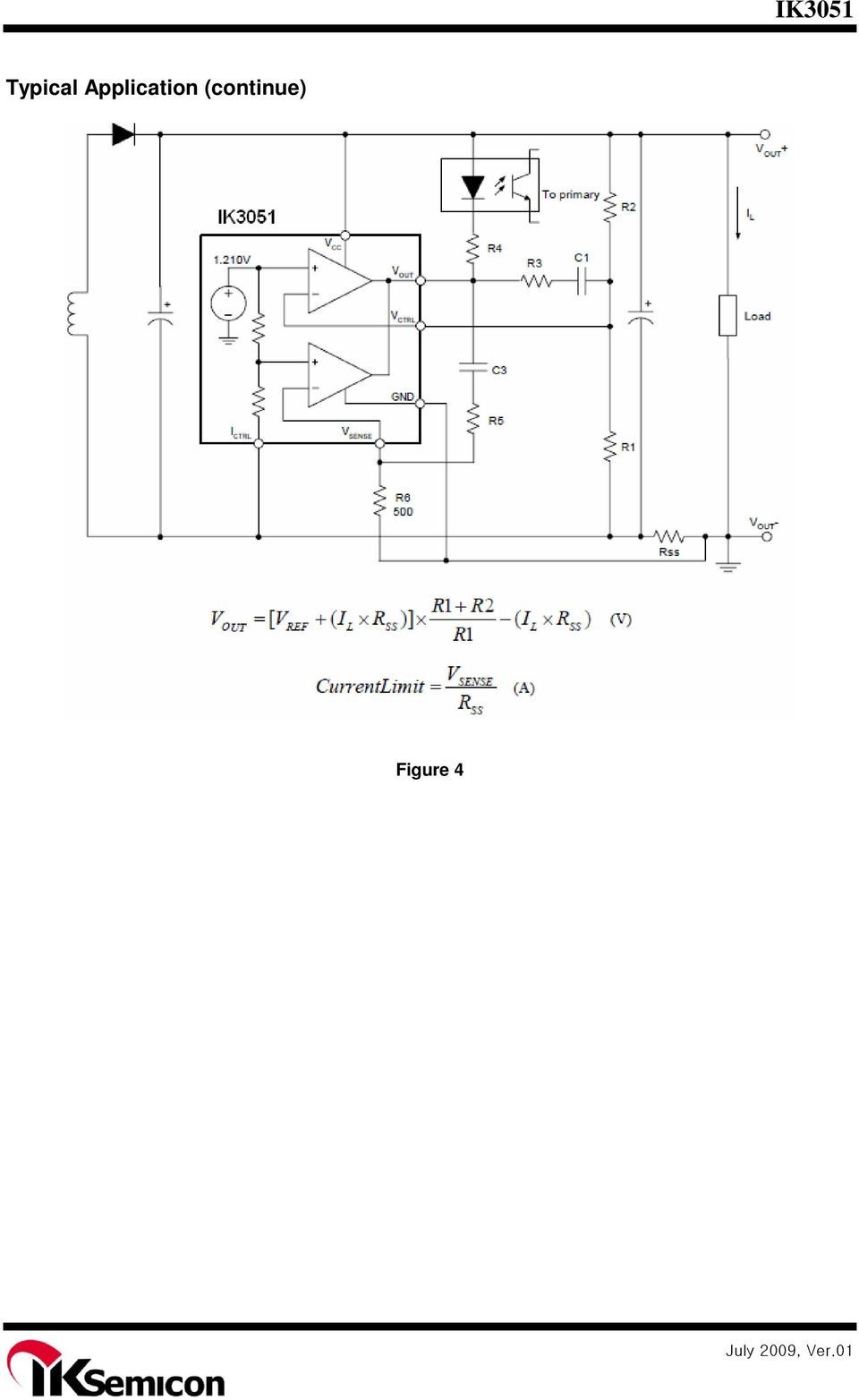
6 Typical Application (continue) Figure 4
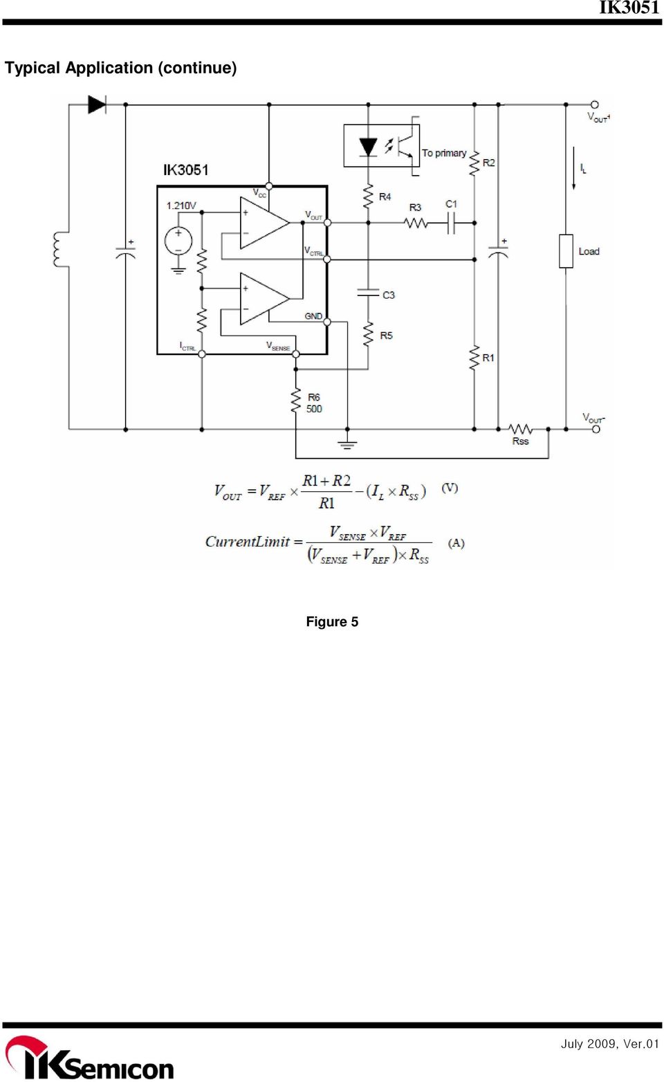
7 Typical Application (continue) Figure 5

8 Typical Performance Characteristics Figure 6: Vref vs Ambient Temperature Figure 7: Vsense pin input bias current vs Ambient Temperature Figure 8: Output short circuit current vs Ambient Temperature Figure 9: Vsense vs Ambient Temperature Figure 10: Ictrl pin input bias current vs Ambient Temperature Figure 11: Supply current vs Ambient Temperature

9 PACKAGE DIMENSION SOT-23-6 Symbol Dimensions In Millimeters Dimensions In Inches Min Max Min Max A A A b c D E E e 0.950TYP 0.037TYP e L 0.600REF 0.024REF L θ

PIN CONFIGURATION FEATURES ORDERING INFORMATION ABSOLUTE MAXIMUM RATINGS. D, F, N Packages
 DESCRIPTION The µa71 is a high performance operational amplifier with high open-loop gain, internal compensation, high common mode range and exceptional temperature stability. The µa71 is short-circuit-protected
28V, 2A Buck Constant Current Switching Regulator for White LED
 28V, 2A Buck Constant Current Switching Regulator for White LED FP7102 General Description The FP7102 is a PWM control buck converter designed to provide a simple, high efficiency solution for driving
TS321 Low Power Single Operational Amplifier
 SOT-25 Pin Definition: 1. Input + 2. Ground 3. Input - 4. Output 5. Vcc General Description The TS321 brings performance and economy to low power systems. With high unity gain frequency and a guaranteed
APPLICATIONS. Battery chargers. DC motor control. Level translating QUANTITY PER REEL. ZXCT1009FTA 7 8mm 3,000 units 109 SOT23
 HIGH-SIDE CURRENT MONITOR DESCRIPTION The is a high side current sense monitor. Using this device eliminates the need to disrupt the ground plane when sensing a load current. It takes a high side voltage
LM741. Single Operational Amplifier. Features. Description. Internal Block Diagram. www.fairchildsemi.com
 Single Operational Amplifier www.fairchildsemi.com Features Short circuit protection Excellent temperature stability Internal frequency compensation High Input voltage range Null of offset Description
High Voltage Current Shunt Monitor AD8212
 High Voltage Current Shunt Monitor AD822 FEATURES Adjustable gain High common-mode voltage range 7 V to 65 V typical 7 V to >500 V with external pass transistor Current output Integrated 5 V series regulator
ADJUSTABLE VOLTAGE AND CURRENT REGULATOR
 L200 ADJUSTABLE VOLTAGE AND CURRENT REGULATOR ADJUSTABLE OUTPUT CURRENT UP TO 2 A (GUARANTEED UP TO Tj = 150 C) ADJUSTABLE OUTPUT VOLTAGE DOWN TO 2.85 V INPUT OVERVOLTAGE PROTECTION (UP TO 60 V, 10 ms)
MC33064DM 5 UNDERVOLTAGE SENSING CIRCUIT
 Order this document by MC3464/D The MC3464 is an undervoltage sensing circuit specifically designed for use as a reset controller in microprocessor-based systems. It offers the designer an economical solution
LM2704 Micropower Step-up DC/DC Converter with 550mA Peak Current Limit
 Micropower Step-up DC/DC Converter with 550mA Peak Current Limit General Description The LM2704 is a micropower step-up DC/DC in a small 5-lead SOT-23 package. A current limited, fixed off-time control
LM56 Dual Output Low Power Thermostat
 Dual Output Low Power Thermostat General Description The LM56 is a precision low power thermostat. Two stable temperature trip points (V T1 and V T2 ) are generated by dividing down the LM56 1.250V bandgap
AP331A XX G - 7. Lead Free G : Green. Packaging (Note 2)
") Features General Description Wide supply Voltage range: 2.0V to 36V Single or dual supplies: ±1.0V to ±18V Very low supply current drain (0.4mA) independent of supply voltage Low input biasing current:
Features General Description Wide supply Voltage range: 2.0V to 36V Single or dual supplies: ±1.0V to ±18V Very low supply current drain (0.4mA) independent of supply voltage Low input biasing current:
Advanced Monolithic Systems
 Advanced Monolithic Systems FEATURES Three Terminal Adjustable or Fixed oltages* 1.5, 1.8, 2.5, 2.85, 3.3 and 5. Output Current of 1A Operates Down to 1 Dropout Line Regulation:.2% Max. Load Regulation:.4%
IPS511/IPS511S FULLY PROTECTED HIGH SIDE POWER MOSFET SWITCH. Load
 Data Sheet No.PD 6155 IPS511/IPS511S FUY PROTECTED IG SIDE POWER MOSFET SWITC Features Over temperature protection (with auto-restart) Short-circuit protection (current limit ) Active clamp E.S.D protection
SG2525A SG3525A REGULATING PULSE WIDTH MODULATORS
 SG2525A SG3525A REGULATING PULSE WIDTH MODULATORS 8 TO 35 V OPERATION 5.1 V REFERENCE TRIMMED TO ± 1 % 100 Hz TO 500 KHz OSCILLATOR RANGE SEPARATE OSCILLATOR SYNC TERMINAL ADJUSTABLE DEADTIME CONTROL INTERNAL
How to Read a Datasheet
 How to Read a Datasheet Prepared for the WIMS outreach program 5/6/02, D. Grover In order to use a PIC microcontroller, a flip-flop, a photodetector, or practically any electronic device, you need to consult
LD7550-B. Green-Mode PWM Controller. General Description. Features. Applications. Typical Application. REV: 01a 12/22/2006 LD7550-B
 12/22/2006 REV: 01a Green-Mode PWM Controller General Description The LD7550-B is a low cost, low startup current, current mode PWM controller with green-mode power-saving operation. The integrated functions
INDUSTRIAL VOLTAGE AMPLIFIER IC AM401 PRINCIPLE FUNCTION
 PINCIPLE FUNCTION Amplification and conversion of differential signals referenced to ground to adjustable industrial voltages (0...Vcc-5V, e.g. 0...5/10V etc.) Variable current/voltage source and integrated
LM138 LM338 5-Amp Adjustable Regulators
 LM138 LM338 5-Amp Adjustable Regulators General Description The LM138 series of adjustable 3-terminal positive voltage regulators is capable of supplying in excess of 5A over a 1 2V to 32V output range
CE8301 Series. Introduction. Features. Ordering Information. Applications SMALL PACKAGE PFM CONTROL STEP-UP DC/DC CONVERTER
 SMALL PACKAGE PFM CONTROL STEP-UP DC/DC CONVERTER Introduction The is a CMOS PFM-control step-up switching DC/DC converter that mainly consists of a reference voltage source, an oscillator, and a comparator.
AAT3520/2/4 MicroPower Microprocessor Reset Circuit
 General Description Features PowerManager The AAT3520 series of PowerManager products is part of AnalogicTech's Total Power Management IC (TPMIC ) product family. These microprocessor reset circuits are
Kit 27. 1W TDA7052 POWER AMPLIFIER
 Kit 27. 1W TDA7052 POWER AMPLIFIER This is a 1 watt mono amplifier Kit module using the TDA7052 from Philips. (Note, no suffix.) It is designed to be used as a building block in other projects where a
Features. Applications
 LM555 Timer General Description The LM555 is a highly stable device for generating accurate time delays or oscillation. Additional terminals are provided for triggering or resetting if desired. In the
High Accuracy, Ultralow IQ, 1 A, anycap Low Dropout Regulator ADP3338
 High Accuracy, Ultralow IQ, 1 A, anycap Low Dropout Regulator ADP3338 FEATURES High accuracy over line and load: ±.8% @ 25 C, ±1.4% over temperature Ultralow dropout voltage: 19 mv (typ) @ 1 A Requires
CLASS-D VERTICAL DEFLECTION AMPLIFIER FOR TV AND MONITOR APPLICATION OUT CFLY + CFLY - BOOT VREG FEEDCAP FREQ. July 2001 1/8
 CLASS-D VERTICAL DEFLECTION AMPLIFIER FOR TV AND MONITOR APPLICATION FEATURES PRELIMINARY DATA HIGH EFFICIENCY POWER AMPLIFIER NO HEATSINK SPLIT SUPPLY INTERNAL FLYBACK GENERATOR OUTPUT CURRENT UP TO.5
LM1084 5A Low Dropout Positive Regulators
 5A Low Dropout Positive Regulators General Description The LM1084 is a series of low dropout voltage positive regulators with a maximum dropout of 1.5 at 5A of load current. It has the same pin-out as
AS2815. 1.5A Low Dropout Voltage Regulator Adjustable & Fixed Output, Fast Response
 1.5A Low Dropout oltage Regulator Adjustable & Fixed Output, Fast Response FEATURES Adjustable Output Down To 1.2 Fixed Output oltages 1.5, 2.5, 3.3, 5.0 Output Current of 1.5A Low Dropout oltage 1.1 Typ.
UC3842/UC3843/UC3844/UC3845
 SMPS Controller www.fairchildsemi.com Features Low Start up Current Maximum Duty Clamp UVLO With Hysteresis Operating Frequency up to 500KHz Description The UC3842/UC3843/UC3844/UC3845 are fixed frequencycurrent-mode
SG6520 FEATURES DESCRIPTION TYPICAL APPLICATION. Product Specification. PC Power Supply Supervisors
 FEATURES Two 12V sense input pins: VS12 and VS12B Over voltage protection (OVP) for 3.3V, 5V and two 12V Over current protection (OCP) for 3.3V, 5V and two 12V Under voltage protection (UVP) for 3.3V,
SPI-8001TW. Switching Regulators. Dual 1.5 A, DC/DC Step-Down Converter. SANKEN ELECTRIC CO., LTD. http://www.sanken-ele.co.jp/en/
 Data Sheet 27469.301.1 Designed to meet high-current requirements at high efficiency in industrial and consumer applications; embedded core, memory, or logic supplies; TVs, VCRs, and office equipment,
KA7500C. SMPS Controller. Features. Description. Internal Block Diagram. www.fairchildsemi.com
 SMPS Controller www.fairchildsemi.com Features Internal Regulator Provides a Stable 5V Reference Supply Trimmed to ±1% Accuracy. Uncommitted Output TR for 200mA Sink or Source Current Output Control for
TDA2822 DUAL POWER AMPLIFIER SUPPLY VOLTAGE DOWN TO 3 V LOW CROSSOVER DISTORSION LOW QUIESCENT CURRENT BRIDGE OR STEREO CONFIGURATION
 TDA2822 DUAL POER AMPLIFIER SUPPLY VOLTAGE DON TO 3 V. LO CROSSOVER DISTORSION LO QUIESCENT CURRENT BRIDGE OR STEREO CONFIGURATION DESCRIPTION The TDA2822 is a monolithic integrated circuit in 12+2+2 powerdip,
LF442 Dual Low Power JFET Input Operational Amplifier
 LF442 Dual Low Power JFET Input Operational Amplifier General Description The LF442 dual low power operational amplifiers provide many of the same AC characteristics as the industry standard LM1458 while
SG6516 PC Power Supply Supervisors
 SG6516 PC Power Supply Supervisors Features Two 12V Sense Input Pins: VS12 and VS12B Over-Voltage Protection (OVP) for 3.3V, 5V, and two 12V Over-Current Protection (OCP) for 3.3V, 5V, and two 12V Under-Voltage
High Speed, Low Power Dual Op Amp AD827
 a FEATURES High Speed 50 MHz Unity Gain Stable Operation 300 V/ms Slew Rate 120 ns Settling Time Drives Unlimited Capacitive Loads Excellent Video Performance 0.04% Differential Gain @ 4.4 MHz 0.198 Differential
NTE2053 Integrated Circuit 8 Bit MPU Compatible A/D Converter
 NTE2053 Integrated Circuit 8 Bit MPU Compatible A/D Converter Description: The NTE2053 is a CMOS 8 bit successive approximation Analog to Digital converter in a 20 Lead DIP type package which uses a differential
Low Voltage, Resistor Programmable Thermostatic Switch AD22105
 a Low Voltage, Resistor Programmable Thermostatic Switch AD22105 FEATURES User-Programmable Temperature Setpoint 2.0 C Setpoint Accuracy 4.0 C Preset Hysteresis Wide Supply Range (+2.7 V dc to +7.0 V dc)
TS34119 Low Power Audio Amplifier
 SOP-8 DIP-8 Pin assignment: 1. CD 8. VO2 2. FC2 7. Gnd 3. FC1 6. Vcc 4. Vin 5. VO1 General Description The TS34119 is a low power audio amplifier, it integrated circuit intended (primarily) for telephone
Constant Current Control for DC-DC Converters
 Constant Current Control for DC-DC Converters Introduction... Theory of Operation... Power Limitations... Voltage Loop Stability...2 Current Loop Compensation...3 Current Control Example...5 Battery Charger
ICS514 LOCO PLL CLOCK GENERATOR. Description. Features. Block Diagram DATASHEET
 DATASHEET ICS514 Description The ICS514 LOCO TM is the most cost effective way to generate a high-quality, high-frequency clock output from a 14.31818 MHz crystal or clock input. The name LOCO stands for
MP2259 1A, 16V, 1.4MHz Step-Down Converter
 MP59 1A, 1V, 1.MHz Step-Down Converter TM The Future of Analog IC Technology DESCRIPTION The MP59 is a monolithic integrated stepdown switch mode converter with an internal power MOSFET. It achieves 1A
LM2901. Low-power quad voltage comparator. Features. Description
 Low-power quad voltage comparator Features Wide single supply voltage range or dual supplies for all devices: +2 V to +36 V or ±1 V to ±18 V Very low supply current (1.1 ma) independent of supply voltage
DATA SHEET. TDA1543 Dual 16-bit DAC (economy version) (I 2 S input format) INTEGRATED CIRCUITS
 (I 2 S input format) INTEGRATED CIRCUITS") INTEGRATED CIRCUITS DATA SHEET File under Integrated Circuits, IC01 February 1991 FEATURES Low distortion 16-bit dynamic range 4 oversampling possible Single 5 V power supply No external components required
INTEGRATED CIRCUITS DATA SHEET File under Integrated Circuits, IC01 February 1991 FEATURES Low distortion 16-bit dynamic range 4 oversampling possible Single 5 V power supply No external components required
TDA4605 CONTROL CIRCUIT FOR SWITCH MODE POWER SUPPLIES USING MOS TRANSISTORS
 CONTROL CIRCUIT FOR SWITCH MODE POWER SUPPLIES USING MOS TRANSISTORS Fold-Back Characteristic provides Overload Protection for External Diodes Burst Operation under Short-Circuit and no Load Conditions
LM386 Low Voltage Audio Power Amplifier
 Low Voltage Audio Power Amplifier General Description The LM386 is a power amplifier designed for use in low voltage consumer applications. The gain is internally set to 20 to keep external part count
Low Noise, Matched Dual PNP Transistor MAT03
 a FEATURES Dual Matched PNP Transistor Low Offset Voltage: 100 V Max Low Noise: 1 nv/ Hz @ 1 khz Max High Gain: 100 Min High Gain Bandwidth: 190 MHz Typ Tight Gain Matching: 3% Max Excellent Logarithmic
TSV6290, TSV6290A, TSV6291, TSV6291A
 Micropower with high merit factor CMOS operational amplifiers Features Low supply voltage: 1.5 V 5.5 V Rail-to-rail input and output Low input offset voltage: 800 µv max (A version) Low power consumption:
UA741. General-purpose single operational amplifier. Features. Applications. Description. N DIP8 (plastic package)
") General-purpose single operational amplifier Datasheet - production data N DIP8 (plastic package) D SO8 (plastic micropackage) Pin connections (top view) 1 - Offset null 1 2 - Inverting input 3 - Non-inverting
General-purpose single operational amplifier Datasheet - production data N DIP8 (plastic package) D SO8 (plastic micropackage) Pin connections (top view) 1 - Offset null 1 2 - Inverting input 3 - Non-inverting
TS555. Low-power single CMOS timer. Description. Features. The TS555 is a single CMOS timer with very low consumption:
 Low-power single CMOS timer Description Datasheet - production data The TS555 is a single CMOS timer with very low consumption: Features SO8 (plastic micropackage) Pin connections (top view) (I cc(typ)
LM2902. Low-power quad operational amplifier. Features. Description
 Low-power quad operational amplifier Datasheet production data Features Wide gain bandwidth: 1.3 MHz Input common-mode voltage range includes negative rail Large voltage gain: 100 db Very low supply current
LM3940 1A Low Dropout Regulator for 5V to 3.3V Conversion
 1A Low Dropout Regulator for 5V to 3.3V Conversion General Description The LM3940 is a 1A low dropout regulator designed to provide 3.3V from a 5V supply. The LM3940 is ideally suited for systems which
IS31LT3360 40V/1.2A LED DRIVER WITH INTERNAL SWITCH. January 2014
 40V/1.2A LED DRIVER WITH INTERNAL SWITCH January 2014 GENERAL DESCRIPTION The IS31LT3360 is a continuous mode inductive step-down converter, designed for driving a single LED or multiple series connected
Features. Ordering Information. * Underbar marking may not be to scale. Part Identification
 MIC86 Teeny Ultra Low Power Op Amp General Description The MIC86 is a rail-to-rail output, input common-mode to ground, operational amplifier in Teeny SC7 packaging. The MIC86 provides 4kHz gain-bandwidth
LM5001 High Voltage Switch Mode Regulator
 High Voltage Switch Mode Regulator General Description The LM5001 high voltage switch mode regulator features all of the functions necessary to implement efficient high voltage Boost, Flyback, SEPIC and
LM1117/LM1117I 800mA Low-Dropout Linear Regulator
 LM1117/LM1117I 800mA Low-Dropout Linear Regulator General Description The LM1117 is a series of low dropout voltage regulators with a dropout of 1.2 at 800mA of load current. It has the same pin-out as
High Accuracy, Ultralow IQ, 1.5 A, anycap Low Dropout Regulator ADP3339
 Data Sheet High Accuracy, Ultralow IQ,.5 A, anycap Low Dropout Regulator FEATURES FUNCTIONAL BLOCK DIAGRAM High accuracy over line and load: ±.9% at 5 C, ±.5% over temperature Ultralow dropout voltage:
LM833 LOW NOISE DUAL OPERATIONAL AMPLIFIER
 LOW NOISE DUAL OPERATIONAL AMPLIFIER LOW VOLTAGE NOISE: 4.5nV/ Hz HIGH GAIN BANDWIDTH PRODUCT: 15MHz HIGH SLEW RATE: 7V/µs LOW DISTORTION:.2% EXCELLENT FREQUENCY STABILITY ESD PROTECTION 2kV DESCRIPTION
Constant voltage and current controller with online digital trimming. Description
 SEA Constant voltage and current controller with online digital trimming Datasheet - production data Redundant OTP (first and second trimming) Extended operating voltage range Very low quiescent current
INTEGRATED CIRCUITS DATA SHEET. TDA7052 1 W BTL mono audio amplifier. Product specification File under Integrated Circuits, IC01
 INTEGRATED CIRCUITS DATA SHEET TDA7052 1 W BTL mono audio amplifier File under Integrated Circuits, IC01 July 1994 GENERAL DESCRIPTION The TDA7052 is a mono output amplifier in a 8-lead dual-in-line (DIL)
LM117 LM317A LM317 3-Terminal Adjustable Regulator
 LM117 LM317A LM317 3-Terminal Adjustable Regulator General Description The LM117 series of adjustable 3-terminal positive voltage regulators is capable of supplying in excess of 1 5A over a 1 2V to 37V
NE555 SA555 - SE555. General-purpose single bipolar timers. Features. Description
 NE555 SA555 - SE555 General-purpose single bipolar timers Features Low turn-off time Maximum operating frequency greater than 500 khz Timing from microseconds to hours Operates in both astable and monostable
Operational Amplifier - IC 741
 Operational Amplifier - IC 741 Tabish December 2005 Aim: To study the working of an 741 operational amplifier by conducting the following experiments: (a) Input bias current measurement (b) Input offset
Programmable Single-/Dual-/Triple- Tone Gong SAE 800
 Programmable Single-/Dual-/Triple- Tone Gong Preliminary Data SAE 800 Bipolar IC Features Supply voltage range 2.8 V to 18 V Few external components (no electrolytic capacitor) 1 tone, 2 tones, 3 tones
LM 358 Op Amp. If you have small signals and need a more useful reading we could amplify it using the op amp, this is commonly used in sensors.
 LM 358 Op Amp S k i l l L e v e l : I n t e r m e d i a t e OVERVIEW The LM 358 is a duel single supply operational amplifier. As it is a single supply it eliminates the need for a duel power supply, thus
www.jameco.com 1-800-831-4242
 Distributed by: www.jameco.com 1-800-831-4242 The content and copyrights of the attached material are the property of its owner. LF411 Low Offset, Low Drift JFET Input Operational Amplifier General Description
High Speed, Low Power Monolithic Op Amp AD847
 a FEATURES Superior Performance High Unity Gain BW: MHz Low Supply Current:.3 ma High Slew Rate: 3 V/ s Excellent Video Specifications.% Differential Gain (NTSC and PAL).9 Differential Phase (NTSC and
STLM20. Ultra-low current 2.4 V precision analog temperature sensor. Features. Applications
 Ultra-low current 2.4 V precision analog temperature sensor Features Precision analog voltage output temperature sensor ±1.5 C maximum temperature accuracy at 25 C (±0.5 C typical) Ultra-low quiescent
NTE923 & NTE923D Integrated Circuit Precision Voltage Regulator
 NTE923 & NTE923D Integrated Circuit Precision Voltage Regulator Description: The NTE923 and NTE923D are voltage regulators designed primarily for series regulator applications. By themselves, these devices
LM139/LM239/LM339/LM2901/LM3302 Low Power Low Offset Voltage Quad Comparators
 Low Power Low Offset Voltage Quad Comparators General Description The LM139 series consists of four independent precision voltage comparators with an offset voltage specification as low as 2 mv max for
LM217M, LM317M. Medium current 1.2 to 37 V adjustable voltage regulator. Description. Features
 Medium current 1.2 to 37 V adjustable voltage regulator Datasheet - production data Description The LM217M and LM317M are monolithic integrated circuits in DPAK package used as positive adjustable voltage
LM118/LM218/LM318 Operational Amplifiers
 LM118/LM218/LM318 Operational Amplifiers General Description The LM118 series are precision high speed operational amplifiers designed for applications requiring wide bandwidth and high slew rate. They
0.9V Boost Driver PR4403 for White LEDs in Solar Lamps
 0.9 Boost Driver for White LEDs in Solar Lamps The is a single cell step-up converter for white LEDs operating from a single rechargeable cell of 1.2 supply voltage down to less than 0.9. An adjustable
NCT3941S/S-A Nuvoton 4 Times Linear Fan Driver NCT3941S/S-A
 Nuvoton 4 Times Linear Fan Driver NCT3941S/S-A -I- Revision A4 Table of Content- 1. GENERAL DESCRIPTION...1 2. FEATURES...1 3. APPLICATION...1 4. BLOCK DIAGRAM...2 5. PIN CONFIGURATION AND TYPICAL APPLICATION
Lab 7: Operational Amplifiers Part I
 Lab 7: Operational Amplifiers Part I Objectives The objective of this lab is to study operational amplifier (op amp) and its applications. We will be simulating and building some basic op amp circuits,
NE555 SA555 - SE555. General-purpose single bipolar timers. Features. Description
 NE555 SA555 - SE555 General-purpose single bipolar timers Features Low turn-off time Maximum operating frequency greater than 500 khz Timing from microseconds to hours Operates in both astable and monostable
Tone Ringer SL2410 LOGIC DIAGRAM PIN ASSIGNMENT SLS
 Tone Ringer The SL2410 is a bipolar integrated circuit designed for telephone bell replacement. Designed for Telephone Bell Replacement Low Curent Drain Adjustable 2-frequency Tone Adjustable Warbling
Discontinued Product For Reference Only
 Data Sheet 29319.12A 2962 DUAL PULSE-WIDTH MODULATED CURRENT CONTROL GROUND IN A SENSE A SINK A SOURCE A THS A V CC SOURCE B SINKB SENSEB IN B THS B 1 2 3 4 5 6 7 8 9 1 11 12 LOGIC LOGIC Dwg. No. D-11
PowerAmp Design. PowerAmp Design PAD135 COMPACT HIGH VOLATGE OP AMP
 PowerAmp Design COMPACT HIGH VOLTAGE OP AMP Rev G KEY FEATURES LOW COST SMALL SIZE 40mm SQUARE HIGH VOLTAGE 200 VOLTS HIGH OUTPUT CURRENT 10A PEAK 40 WATT DISSIPATION CAPABILITY 200V/µS SLEW RATE APPLICATIONS
MP1541 1.3MHz Boost Converter
 MP5.3MHz Boost Converter The Future of Analog IC Technology DESCRIPTION The MP5 is a 5-pin thin SOT3 current mode step up converter intended for small, low power applications. The MP5 switches at.3mhz
Design of a TL431-Based Controller for a Flyback Converter
 Design of a TL431-Based Controller for a Flyback Converter Dr. John Schönberger Plexim GmbH Technoparkstrasse 1 8005 Zürich 1 Introduction The TL431 is a reference voltage source that is commonly used
High Performance Current Mode PWM Controller Cycle Turning + POWER FROM LIEMIC. For, 2008 LIEMIC Semiconductor Co.,Ltd. LN3C63AD REV: 1.0.
 LN3C63 High Performance Current Mode PWM Controller Cycle Turning + POWER FROM LIEMIC For, Adaptor & Charger Offline Power Supply Open Frame Power DVD&DVB Player Auxiliary Power for PC etc..... 2008 LIEMIC
School of Engineering Department of Electrical and Computer Engineering
 1 School of Engineering Department of Electrical and Computer Engineering 332:223 Principles of Electrical Engineering I Laboratory Experiment #4 Title: Operational Amplifiers 1 Introduction Objectives
ICS379. Quad PLL with VCXO Quick Turn Clock. Description. Features. Block Diagram
 Quad PLL with VCXO Quick Turn Clock Description The ICS379 QTClock TM generates up to 9 high quality, high frequency clock outputs including a reference from a low frequency pullable crystal. It is designed
DATA SHEET. TDA8560Q 2 40 W/2 Ω stereo BTL car radio power amplifier with diagnostic facility INTEGRATED CIRCUITS. 1996 Jan 08
 INTEGRATED CIRCUITS DATA SHEET power amplifier with diagnostic facility Supersedes data of March 1994 File under Integrated Circuits, IC01 1996 Jan 08 FEATURES Requires very few external components High
LDS8720. 184 WLED Matrix Driver with Boost Converter FEATURES APPLICATION DESCRIPTION TYPICAL APPLICATION CIRCUIT
 184 WLED Matrix Driver with Boost Converter FEATURES High efficiency boost converter with the input voltage range from 2.7 to 5.5 V No external Schottky Required (Internal synchronous rectifier) 250 mv
FEATURES DESCRIPTION APPLICATIONS BLOCK DIAGRAM. PT2248 Infrared Remote Control Transmitter
 Infrared Remote Control Transmitter DESCRIPTION PT2248 is an infrared remote control transmitter utilizing CMOS Technology. It is capable of 18 functions and a total of 75 commands. Single-shot and continuous
SD4840/4841/4842/4843/4844
 CURRENT MODE PWM CONTROLLER WITH BUILT-IN HIGH VOLTAGE MOSFET DESCRIPTION SD4840/4841/4842/4843/4844 is a current mode PWM controller with low standby power and low start current for power switch. In standby
TL084 TL084A - TL084B
 A B GENERAL PURPOSE JFET QUAD OPERATIONAL AMPLIFIERS WIDE COMMONMODE (UP TO V + CC ) AND DIFFERENTIAL VOLTAGE RANGE LOW INPUT BIAS AND OFFSET CURRENT OUTPUT SHORTCIRCUIT PROTECTION HIGH INPUT IMPEDANCE
STLQ015. 150 ma, ultra low quiescent current linear voltage regulator. Description. Features. Application
 150 ma, ultra low quiescent current linear voltage regulator Description Datasheet - production data Features SOT23-5L Input voltage from 1.5 to 5.5 V Very low quiescent current: 1.0 µa (typ.) at no load
LF412 Low Offset Low Drift Dual JFET Input Operational Amplifier
 LF412 Low Offset Low Drift Dual JFET Input Operational Amplifier General Description These devices are low cost high speed JFET input operational amplifiers with very low input offset voltage and guaranteed
WHITE LED STEP-UP CONVERTER. Features
 General Description The is an inductor-based DC/DC converter designed to drive up to eight white LEDs in series for backlight. Only one feedback resistor is needed to control the LED current and obtain
SWITCH-MODE POWER SUPPLY CONTROLLER PULSE OUTPUT DC OUTPUT GROUND EXTERNAL FUNCTION SIMULATION ZERO CROSSING INPUT CONTROL EXTERNAL FUNCTION
 SWITCH-MODE POWER SUPPLY CONTROLLER. LOW START-UP CURRENT. DIRECT CONTROL OF SWITCHING TRAN- SISTOR. COLLECTOR CURRENT PROPORTIONAL TO BASE-CURRENT INPUT REERSE-GOING LINEAR OERLOAD CHARACTERISTIC CURE
TLI4946. Datasheet TLI4946K, TLI4946-2K, TLI4946-2L. Sense and Control. May 2009
 May 2009 TLI4946 High Precision Hall Effect Latches for Industrial and Consumer Applications TLI4946K, TLI4946-2K, TLI4946-2L Datasheet Rev. 1.0 Sense and Control Edition 2009-05-04 Published by Infineon
1A L.D.O VOLTAGE REGULATOR
 FEATURES Output Current up to 1 A Low Dropout Voltage (1.2V at 1A Output current) Three Terminal Adjustable(ADJ) or Fixed 1.2V, 1.5V, 1.8V, 2.5V, 2.85V, 5.0V Line Regulation typically at 0.1% max. Load
BJT Characteristics and Amplifiers
 BJT Characteristics and Amplifiers Matthew Beckler [email protected] EE2002 Lab Section 003 April 2, 2006 Abstract As a basic component in amplifier design, the properties of the Bipolar Junction Transistor
LM78XX Series Voltage Regulators
 LM78XX Series Voltage Regulators General Description Connection Diagrams The LM78XX series of three terminal regulators is available with several fixed output voltages making them useful in a wide range
1.5A Ultra Low Dropout Linear Regulator TJ3965
 FEATURES Ultra Low Dropout Voltage Low Ground Pin Current Excellent Line and Load Regulation Guaranteed Output Current of 1.5A Available in MSOP8, SOP8, SOP8PP, SOT223, TO252, TO263, TO220, and SOT89 Packages
LM555/NE555/SA555. Single Timer. Description. Features. Applications. Internal Block Diagram. Vcc GND. Trigger. Discharge. Output F/F.
 Single Timer www.fairchildsemi.com Features High Current Drive Capability (00mA) Adjustable Duty Cycle Temperature Stability of 0.005%/ C Timing From µsec to Hours Turn off Time Less Than µsec Applications
DUAL FULL-BRIDGE PWM MOTOR DRIVER
 9 Data Sheet 99.0F PWM OUT A OUT A E SENSE OUT B UDN9B (DP) 0 9 LOAD SUPPLY E SENSE OUT B The UDN9B, UDN9EB, and UDN9LB motor drivers are designed to drive both windings of a bipolar stepper motor or bidirectionally
LM350. 3.0 A, Adjustable Output, Positive Voltage Regulator THREE TERMINAL ADJUSTABLE POSITIVE VOLTAGE REGULATOR
 3. A, able Output, Positive Voltage Regulator The is an adjustable threeterminal positive voltage regulator capable of supplying in excess of 3. A over an output voltage range of 1.2 V to 33 V. This voltage
DESCRIPTION FEATURES BLOCK DIAGRAM. PT2260 Remote Control Encoder
 Remote Control Encoder DESCRIPTION PT2260 is a remote control encoder paired with either PT2270 or PT2272 utilizing CMOS Technology. It encodes data and address pins into a serial coded waveform suitable