Lecture : 9 Carbon Nanotubes and Carbon Nanotube transistors. S. E. Thompson Fall 2004
|
|
|
- Eugene Craig
- 9 years ago
- Views:
Transcription

1 1 Lecture : 9 Carbon Nanotubes and Carbon Nanotube transistors S. E. Thompson Fall 2004

2 Ref. P. Wong, IBM 2

3 Ken David, Intel 3
4 Nanoelectronics Now or Never?" IEDM Evening Panel Discussion, December 14, 4 Session 26: 8:00 p.m. Continental Ballroom 6-9 Moderator: Mark Lundstrom, Purdue University "Nanoelectronics Now or Never?" Traditional 'top-down' microelectronics has become nanoelectronics with device dimensions comparable to those being explored in the new field of ëbottom-up' nano- and molecular electronics. We use the terms, top-down and bottom-up, in a very general sense. Top-down refers to a way of thinking and building that begins at the macro (continuum) scale and pushes to the nanoscale. Bottom-up refers to a way of thinking and building that begins at the atomistic level and builds up to the nanoscale. The top-down approach has already delivered silicon MOSFETs with channel lengths of ~ 5nm, but scaling down device dimensions with commensurate increase in device and system performance is increasingly challenging. Bottom-up technology has demonstrated molecular switches, nanotube and nanowire FET's, NDR and single electron devices, and ultradense memory prototypes. Is bottom-up nanotechnology ready to address the industry's challenges, or is it still long-term research with essentially unpredictable outcomes? This panel will debate the question of what the intersection of top-down and bottom-up electronics will mean to semiconductor technology of the future.

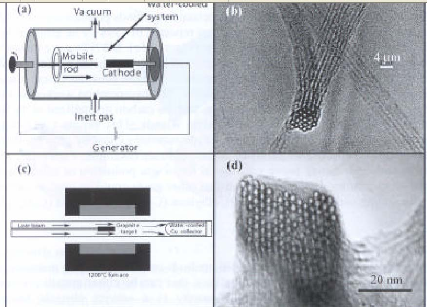
5 Carbon Nanotube Growth 5
6 Reason Carbon Nanotubes are Interesting 6 Fundamental physics and chemistry changes when the dimensions of a solid becomes comparable to one or more of these characteristic lengths, many of which are in the nanometer range. Example: Size of semiconducting material is in the order of the wavelength of the electrons and holes. Electronic structure and transport completely changes

7 Roll Carbon Nanotube from Graphite 7 Ref: Intro to Nanotechnology
8 Constructing Nanotubes from a Graphene Sheet 8 Chiral angle Zigzag 0,0 1,0 2,0 3,0 4,0 5,0 6,0 7,0 8,0 9,0 10,0 11,0 12,0 13,0 1,1 1,1 3,1 4,1 5,1 6,1 7,1 8,1 9,1 10,1 11,1 12,1 13,1 Roll-up vector 2,2 3,2 4,2 5,2 6,2 7,2 8,2 9,2 10,2 11,2 12,2 3,3 4,3 5,3 6,3 7,3 8,3 9,3 10,3 11,3 12,3 Armchair 4,4 5,4 6,4 7,4 8,4 9,4 10,4 11,4 5,5 6,5 7,5 8,5 9,5 10,5 11,5 a 1 6,6 7,6 8,6 9,6 10,6 a 2 7,7 8,7 9,7 10,7 8,8 9,8
9 9 Semiconductor nanotubes 2,0 3,1 4,2 5,3 6,4 7,5 8,6 9,7 10,8 11,9 5,0 6,1 7,2 8,3 9,4 10,5 11,6 12,7 8,0 9,1 10,2 11,3 12,4 13,5 11,0 12,1 13,2 14,3 14,0 15,1 1,0 2,1 3,2 4,3 5,4 6,5 7,6 8,7 9,8 10,9 11,10 4,0 5,1 6,2 7,3 8,4 9,5 10,6 11,7 12,8 7,0 8,1 9,2 10,3 11,4 12,5 13,6 10,0 11,1 12,2 13,3 14,4 13,0 14,1 15,2 16,0 10,9 9,8 8,7 7,6 6,5 5,4 10,6 9,5 8,4 12,5 11,4 10,3 9,2 13,3 12,2 11,1 10,8 9,7 8,6 7,5 6,4 11,6 10,5 9,4 8,3 13,5 12,4 11,3 10,2 9,1 13,2 12,1 15,1 zigzag armchair 1.0 nm diameter
10 Some More Properties of Nanotubes 10 1 to 10 nm diameters 10 of um long End capped with half a fullerence molecule Single and multi-wall nanotubes Chirality refers to how the tubes are rolled One-third metallic two-thirds semiconductor Energy gap: 1/(diameter of tube) Diameter of tube increases, bandgap decreases

11 Extension of C 60, C 70, C End closed 11

12 Multi Wall Tubes 12

13 Bandgap of Semiconductor Tube 13
14 s and p Wavefunctions 14 Ref: Intro to Nanotechnology
15 Carbon Nanotubes: Fullfill Requirements For a Logic Device? 15 Non-linear characteristics Power amplification Concatenability Feedback prevention Basic Logic

16 C Ref: Intro to Nanotechnology

17 Closed Network From Other Atoms 17 Ref: Intro to Nanotechnology

18 Si Nano Wires Converted to NiSi 18 Si nanowire Lieber, Nature 2004

19 Si Nano Wire Transistors 19 Lieber, Nature 2004
20 Carbon Nanotubes: Fullfill Requirements For a Logic Device? 20 Non-linear characteristics Power amplification Concatenability Feedback prevention Basic Logic
21 Summary 21
22 22

23 23

24 24

25 25

26 26
27 27
28 28
29 29

30 30

31 31

32 32
33 33
34 34
35 Carbon Nanotube Lectures 35 What are Carbon Nanotubes and Transistors Metrology Used to Measure Nanotubes Mass spectrometer Transmission Electron Microscopy Scanning Microscopy Scanning electron microscope Scanning tunneling microscope Atomic force microscope How nanotubes are grown Carbon Nanotube Electronic Properties Carbon Nanotube State of the Art Transistors Carbon Nanotube Integration Carbon Nanotube Potential Future Applications Nobel Prize winner Prof. Richard Smalley Lecture on Nanotubes

36 References 36 Chapter: Carbon nanotube for data processing
37 What is a Carbon Nanotude Transistor 37

38 Ref: Jing Guo 38

39 Nanotechnology 39 The Principles of Physics, as far as I can see, do not speak against the possibility of Maneuvering things atom by atom. It is not an Attempt to violate any laws; it is something, in Principle, that can be done; but in practice, it Has not been done because we are too big Richard Feynman
40 Nanotechnology History 1959 Plenty of Room at the Bottom Richard Feynman Lecture given to American Physical Society Feynman envisioned Etching lines a few atoms wide Patterning with e-beam Manipulating individual atoms (scanning tunneling microscope) Building circuits on nanometer scale Nanostructures already present in biological systems 40
41 Micro and Nano History 1 Micro and Nano History Scanning tunneling microscope (STM) Heinrich Rohler and Gerd Karl Binning Buckyballs discovered Richard Smalley, Robert Curl, Jr., Harold Kroto 1986 Atomic Force Microscope (AFM) 1991 Carbon Nanotube discovered as part of ERATO program in Japan ( ) Sumio Ijima 1996 NSF commissioned nanoscience and nanotechnology study Recommned National Nanotechnology Initiative 2001 Nanotube logic demonstrated with carbon nanotubes 41
42 What is a Carbon Nanotube? 42 Start with Carbon Graphite C 60 Single Wall Carbon Nanotubes Multi Wall Carbon Nanotubes Carbon Nanotube Transistors
43 Start with Carbon 43 Carbon contains six electrons (1s) 2, 2s, 2px,2py, 2pz 1s quantum number N=1 (2 electrons) N=2, four electrons s orbital spherically symmetric about nucleous p directed charge distribution s and p form chemical bond Ψ = s + λp Solid carbon two main structures Diamond sp degree bonds Graphitic sheet sp degree bonds. Each bond in same plane Graphite s, px, py Sheets held together by weaker van der Waals Forces
44 Discovery of C Soccer ball-like molecule containing 60 carbon atoms Motivated by understanding ligh transmission through interstellar dust Optical extinction: absorption and scattering of light from interstellar dust C60 envisioned by theoretical chemist High powered pulsed laser simulate conditions of hot carbon Prof. Richard Smalley (Rice) observed mass number 720 mass spectrometer (carbon mass #12) Smalley won Nobel prize

45 ATM or STM Used to Determine Chirality 45
What is Nanophysics: Survey of Course Topics. Branislav K. Nikolić
 What is Nanophysics: Survey of Course Topics Branislav K. Nikolić Department of Physics and Astronomy, University of Delaware, Newark, DE 19716, U.S.A. http://wiki.physics.udel.edu/phys824 Definition of
Usage of Carbon Nanotubes in Scanning Probe Microscopes as Probe. Keywords: Carbon Nanotube, Scanning Probe Microscope
 International Journal of Arts and Sciences 3(1): 18-26 (2009) CD-ROM. ISSN: 1944-6934 InternationalJournal.org Usage of Carbon Nanotubes in Scanning Probe Microscopes as Probe Bedri Onur Kucukyildirim,
CS257 Introduction to Nanocomputing
 CS257 Introduction to Nanocomputing Overview of Crossbar-Based Computing John E Savage Overview Intro to NW growth methods Chemical vapor deposition and fluidic assembly Nano imprinting Nano stamping Four
Nanoscience Course Descriptions
 Nanoscience Course Descriptions NANO*1000 Introduction to Nanoscience This course introduces students to the emerging field of nanoscience. Its representation in popular culture and journalism will be
Matter, Materials, Crystal Structure and Bonding. Chris J. Pickard
 Matter, Materials, Crystal Structure and Bonding Chris J. Pickard Why should a theorist care? Where the atoms are determines what they do Where the atoms can be determines what we can do Overview of Structure
Highlights of Solid State Physics. Man of the Year Nobel Prizes
 Highlights of Solid State Physics Man of the Year Nobel Prizes Silicon Technology Moore s Law Gordon Moore Intel Jack Kilby 14 nm 2014 Physics Nobel Prize 2000 Integrated Circuit Electrons in the Conduction
Nanocomputer & Architecture
 Nanocomputer & Architecture Yingjie Wei Western Michigan University Department of Computer Science CS 603 - Dr. Elise dedonckor Febrary 4 th, 2004 Nanocomputer Architecture Contents Overview of Nanotechnology
Nanoelectronics 09. Atsufumi Hirohata Department of Electronics. Quick Review over the Last Lecture
 Nanoelectronics 09 Atsufumi Hirohata Department of Electronics 12:00 Wednesday, 4/February/2015 (P/L 006) Quick Review over the Last Lecture ( Field effect transistor (FET) ): ( Drain ) current increases
www.keithley.com 1 st Edition Nanotechnology Measurement Handbook A Guide to Electrical Measurements for Nanoscience Applications
 www.keithley.com 1 st Edition Nanotechnology Measurement Handbook A Guide to Electrical Measurements for Nanoscience Applications To get a free electronic version of this book, visit Keithley s Knowledge
Solid State Electronics and Photonics Electrical and Computer Engineering The Ohio State University
 Solid State Electronics and Photonics Electrical and Computer Engineering The Ohio State University An Overview for Prospective Students http://www.ece.osu.edu/ssep SSEP Area: Who Are We? First Row Betty
Nano Technology for Computer Science: Scope and Opportunities
 International Journal of Electronic and Electrical Engineering. ISSN 0974-2174, Volume 7, Number 3 (2014), pp. 213-218 International Research Publication House http://www.irphouse.com Nano Technology for
Carbon-Carbon bonds: Hybridization
 Carbon-Carbon bonds: Hybridization Abstract: Gina 05/05/11 Molecular binding behavior has a large inuence on the structure of a material and their properties. As a exclusion, carbon bind themself not in
Basic principles and mechanisms of NSOM; Different scanning modes and systems of NSOM; General applications and advantages of NSOM.
 Lecture 16: Near-field Scanning Optical Microscopy (NSOM) Background of NSOM; Basic principles and mechanisms of NSOM; Basic components of a NSOM; Different scanning modes and systems of NSOM; General
Lecture 4 Scanning Probe Microscopy (SPM)
") Lecture 4 Scanning Probe Microscopy (SPM) General components of SPM; Tip --- the probe; Cantilever --- the indicator of the tip; Tip-sample interaction --- the feedback system; Scanner --- piezoelectric
Lecture 4 Scanning Probe Microscopy (SPM) General components of SPM; Tip --- the probe; Cantilever --- the indicator of the tip; Tip-sample interaction --- the feedback system; Scanner --- piezoelectric
Lecture 6 Scanning Tunneling Microscopy (STM) General components of STM; Tunneling current; Feedback system; Tip --- the probe.
 General components of STM; Tunneling current; Feedback system; Tip --- the probe.") Lecture 6 Scanning Tunneling Microscopy (STM) General components of STM; Tunneling current; Feedback system; Tip --- the probe. Brief Overview of STM Inventors of STM The Nobel Prize in Physics 1986 Nobel
Lecture 6 Scanning Tunneling Microscopy (STM) General components of STM; Tunneling current; Feedback system; Tip --- the probe. Brief Overview of STM Inventors of STM The Nobel Prize in Physics 1986 Nobel
Nano-Spectroscopy. Solutions AFM-Raman, TERS, NSOM Chemical imaging at the nanoscale
 Nano-Spectroscopy Solutions AFM-Raman, TERS, NSOM Chemical imaging at the nanoscale Since its introduction in the early 80 s, Scanning Probe Microscopy (SPM) has quickly made nanoscale imaging an affordable
Modification of Graphene Films by Laser-Generated High Energy Particles
 Modification of Graphene Films by Laser-Generated High Energy Particles Elena Stolyarova (Polyakova), Ph.D. ATF Program Advisory and ATF Users Meeting April 2-3, 2009, Berkner Hall, Room B, BNL Department
Atoms, Ions and Molecules The Building Blocks of Matter
 Atoms, Ions and Molecules The Building Blocks of Matter Chapter 2 1 Chapter Outline 2.1 The Rutherford Model of Atomic Structure 2.2 Nuclides and Their Symbols 2.3 Navigating the Periodic Table 2.4 The
Laser Based Micro and Nanoscale Manufacturing and Materials Processing
 Laser Based Micro and Nanoscale Manufacturing and Materials Processing Faculty: Prof. Xianfan Xu Email: [email protected] Phone: (765) 494-5639 http://widget.ecn.purdue.edu/~xxu Research Areas: Development
Atomic Force Microscopy. Long Phan Nanotechnology Summer Series May 15, 2013
 Atomic Force Microscopy Long Phan Nanotechnology Summer Series May 15, 2013 1 World s Smallest Movie 2 Outline What is AFM? How does AFM Work? 3 Modes: Contact mode Non contact mode Tapping mode Imaging
Chemical Synthesis. Overview. Chemical Synthesis of Nanocrystals. Self-Assembly of Nanocrystals. Example: Cu 146 Se 73 (PPh 3 ) 30
 30") Chemical Synthesis Spontaneous organization of molecules into stable, structurally well-defined aggregates at the nanometer length scale. Overview The 1-100 nm nanoscale length is in between traditional
Chemical Synthesis Spontaneous organization of molecules into stable, structurally well-defined aggregates at the nanometer length scale. Overview The 1-100 nm nanoscale length is in between traditional
NANOTECHNOLOGY BACKGROUND
 NANOTECHNOLOGY BACKGROUND Introduction and Overview Nanotechnology is defined as the study of the fundamental laws and theories of atoms and structures that have critical dimensions between 1 and 100 nanometers.
NANOSCALE SCIENCE AND ENGINEERING: MATERIALS, ELECTRONICS, PHOTONICS, BIOSENSORS AND BEYOND
 Inversion mode MOSFET p- pn junction Silicon film (n- type) Gate Silicon film (p- type) Gate oxide Continuing Education Program (CEP) on NANOSCALE SCIENCE AND ENGINEERING: MATERIALS, ELECTRONICS, PHOTONICS,
The Application of Density Functional Theory in Materials Science
 The Application of Density Functional Theory in Materials Science Slide 1 Outline Atomistic Modelling Group at MUL Density Functional Theory Numerical Details HPC Cluster at the MU Leoben Applications
It has long been a goal to achieve higher spatial resolution in optical imaging and
 Nano-optical Imaging using Scattering Scanning Near-field Optical Microscopy Fehmi Yasin, Advisor: Dr. Markus Raschke, Post-doc: Dr. Gregory Andreev, Graduate Student: Benjamin Pollard Department of Physics,
Atoms, Ions and Molecules The Building Blocks of Matter
 Atoms, Ions and Molecules The Building Blocks of Matter Chapter 2 1 Chapter Outline 2.1 The Rutherford Model of Atomic Structure 2.2 Nuclides and Their Symbols 2.3 Navigating the Periodic Table 2.4 The
nanohub.org Toward On-Line Simulation for Materials and Nanodevices by Design
 Univ. of Florida, Univ. of Illinois, Morgan State Univ., Northwestern Univ. Purdue Univ. Stanford Univ., UTEP nanohub.org Toward On-Line Simulation for Materials and Nanodevices by Design 1 Gerhard Klimeck,
New materials on horizon for advanced logic technology in mobile era
 New materials on horizon for advanced logic technology in mobile era source gate Kelin J. Kuhn, TED 2012 drain Franz Kreupl, IFX 2003 Hsinchu March 6, 2013 - Prof. Dr. Franz Kreupl 1 Outline Introduction
Nanotechnology and Its Impact on Modern Computer
 Global Journal of Researches in Engineering General Engineering Volume 12 Issue 4 Version 1.0 Year 2012 Type: Double Blind Peer Reviewed International Research Journal Publisher: Global Journals Inc. (USA)
Electronic Transport in Ropes of Single Wall Carbon Nanotubes
 Electronic Transport in Ropes of Single Wall Carbon Nanotubes Von der Fakultät für Mathematik, Informatik und Naturwissenschaften der Rheinisch-Westfälischen Technischen Hochschule Aachen zur Erlangung
From Nano-Electronics and Photonics to Renewable Energy
 From Nano-Electronics and Photonics to Renewable Energy Tom Smy Department of Electronics, Carleton University Questions are welcome! OUTLINE Introduction: to EE and Engineering Physics Renewable Energy
Graphene a material for the future
 Graphene a material for the future by Olav Thorsen What is graphene? What is graphene? Simply put, it is a thin layer of pure carbon What is graphene? Simply put, it is a thin layer of pure carbon It has
Introduction to Nanotechnology - History, Definition, Methodology, Applications, and Challenges. Instructor: Dr. Yu-Bin Chen Date: 07/25/2012
 Introduction to Nanotechnology - History, Definition, Methodology, Applications, and Challenges Instructor: Dr. Yu-Bin Chen Date: 07/25/2012 Outline Outline History Definition Methodology Applications
Crystalline solids. A solid crystal consists of different atoms arranged in a periodic structure.
 Crystalline solids A solid crystal consists of different atoms arranged in a periodic structure. Crystals can be formed via various bonding mechanisms: Ionic bonding Covalent bonding Metallic bonding Van
Atomic Force Microscopy. July, 2011 R. C. Decker and S. Qazi
 Atomic Force Microscopy July, 2011 R. C. Decker and S. Qazi Learning through Visualization Visualization of physical phenomena can confirm hypothesis Observation provides opportunities for study without
Predicted Performance Advantages of Carbon Nanotube Transistors with Doped Nanotubes as Source/Drain
 Predicted Performance Advantages of Carbon Nanotube Transistors with Doped Nanotubes as Source/Drain Jing Guo, Ali Javey, Hongjie Dai, Supriyo Datta and Mark Lundstrom School of ECE, Purdue University,
7/3/2014. Introduction to Atomic Force Microscope. Introduction to Scanning Force Microscope. Invention of Atomic Force Microscope (AFM)
") Introduction to Atomic Force Microscope Introduction to Scanning Force Microscope Not that kind of atomic Tien Ming Chuang ( 莊 天 明 ) Institute of Physics, Academia Sinica Tien Ming Chuang ( 莊 天 明 ) Institute
Introduction to Atomic Force Microscope Introduction to Scanning Force Microscope Not that kind of atomic Tien Ming Chuang ( 莊 天 明 ) Institute of Physics, Academia Sinica Tien Ming Chuang ( 莊 天 明 ) Institute
KINETIC THEORY AND THERMODYNAMICS
 KINETIC THEORY AND THERMODYNAMICS 1. Basic ideas Kinetic theory based on experiments, which proved that a) matter contains particles and quite a lot of space between them b) these particles always move
- particle with kinetic energy E strikes a barrier with height U 0 > E and width L. - classically the particle cannot overcome the barrier
 Tunnel Effect: - particle with kinetic energy E strikes a barrier with height U 0 > E and width L - classically the particle cannot overcome the barrier - quantum mechanically the particle can penetrated
Polarization Dependence in X-ray Spectroscopy and Scattering. S P Collins et al Diamond Light Source UK
 Polarization Dependence in X-ray Spectroscopy and Scattering S P Collins et al Diamond Light Source UK Overview of talk 1. Experimental techniques at Diamond: why we care about x-ray polarization 2. How
LabRAM HR. Research Raman Made Easy! Raman Spectroscopy Systems. Spectroscopy Suite. Powered by:
 LabRAM HR Research Raman Made Easy! Raman Spectroscopy Systems Powered by: Spectroscopy Suite Cutting-Edge Applications with the LabRAM HR Deeply involved in Raman spectroscopy for decades, HORIBA Scientific
Hybrid Molecular Orbitals
 Hybrid Molecular Orbitals Last time you learned how to construct molecule orbital diagrams for simple molecules based on the symmetry of the atomic orbitals. Molecular orbitals extend over the entire molecule
NANOCAP Nanotechnology Capacity Building NGOs
 NANOCAP Nanotechnology Capacity Building NGOs Nanotechnology: A BRIEF INTRODUCTION Luisa Filipponi & Duncan Sutherland Interdisciplinary Nanoscience Center (inano) University of Aarhus, Denmark NOTE: This
Bio@IT Lisboa, July 2, 2012. Bioelectronics. Luís Alcácer. 2005, it - instituto de telecomunicações. Todos os direitos reservados.
 Lisboa, July 2, 2012 Luís Alcácer 2005, it - instituto de telecomunicações. Todos os direitos reservados. Outline Organic Organic Nanoelectronics Molecular Electronics 2 July 2, 2012 Lisboa Sensu lato
Microscopy: Principles and Advances
 Microscopy: Principles and Advances Chandrashekhar V. Kulkarni University of Central Lancashire, Preston, United kingdom May, 2014 University of Ljubljana Academic Background 2005-2008: PhD-Chemical Biology
Unit 12 Practice Test
 Name: Class: Date: ID: A Unit 12 Practice Test Multiple Choice Identify the choice that best completes the statement or answers the question. 1) A solid has a very high melting point, great hardness, and
Scanning Probe Microscopy
 Ernst Meyer Hans Josef Hug Roland Bennewitz Scanning Probe Microscopy The Lab on a Tip With 117 Figures Mß Springer Contents 1 Introduction to Scanning Probe Microscopy f f.1 Overview 2 f.2 Basic Concepts
LabRAM HR Evolution. Research Raman Made Easy!
 LabRAM HR Evolution Research Raman Made Easy! Cutting-Edge Applications with the LabRAM HR LabRAM HR Deeply involved in Raman spectroscopy for decades, HORIBA Scientific has been providing an extensive
Optical Hyperdoping: Transforming Semiconductor Band Structure for Solar Energy Harvesting
 Optical Hyperdoping: Transforming Semiconductor Band Structure for Solar Energy Harvesting 3G Solar Technologies Multidisciplinary Workshop MRS Spring Meeting San Francisco, CA, 5 April 2010 Michael P.
Lecture 3: Optical Properties of Bulk and Nano. 5 nm
 Lecture 3: Optical Properties of Bulk and Nano 5 nm The Previous Lecture Origin frequency dependence of χ in real materials Lorentz model (harmonic oscillator model) 0 e - n( ) n' n '' n ' = 1 + Nucleus
Nanometer-scale imaging and metrology, nano-fabrication with the Orion Helium Ion Microscope
 [email protected] Nanometer-scale imaging and metrology, nano-fabrication with the Orion Helium Ion Microscope Bin Ming, András E. Vladár and Michael T. Postek National Institute of Standards and Technology
Read the sections on Allotropy and Allotropes in your text (pages 464, 475, 871-2, 882-3) and answer the following:
 and answer the following:") Descriptive Chemistry Assignment 5 Thermodynamics and Allotropes Read the sections on Allotropy and Allotropes in your text (pages 464, 475, 871-2, 882-3) and answer the following: 1. Define the word allotrope
Descriptive Chemistry Assignment 5 Thermodynamics and Allotropes Read the sections on Allotropy and Allotropes in your text (pages 464, 475, 871-2, 882-3) and answer the following: 1. Define the word allotrope
A METHOD OF PRECISE CALIBRATION FOR PIEZOELECTRICAL ACTUATORS
 Uludağ Üniversitesi Mühendislik-Mimarlık Fakültesi Dergisi, Cilt 9, Sayı, 24 A METHOD OF PRECISE CALIBRATION FOR PIEZOELECTRICAL ACTUATORS Timur CANEL * Yüksel BEKTÖRE ** Abstract: Piezoelectrical actuators
Electrical properties of Carbon Nanotubes
 Electrical properties of Carbon Nanotubes Kasper Grove-Rasmussen Thomas Jørgensen August 28, 2000 1 Contents 1 Preface 3 2 Introduction to Carbon Nanotubes 4 3 Single wall Carbon Nanotubes 5 4 Reciprocal
Nanoscale Resolution Options for Optical Localization Techniques. C. Boit TU Berlin Chair of Semiconductor Devices
 berlin Nanoscale Resolution Options for Optical Localization Techniques C. Boit TU Berlin Chair of Semiconductor Devices EUFANET Workshop on Optical Localization Techniques Toulouse, Jan 26, 2009 Jan 26,
Design of 2D waveguide networks for the study of fundamental properties of Quantum Graphs
 Design of 2D waveguide networks for the study of fundamental properties of Quantum Graphs Introduction: what is a quantum graph? Areas of application of quantum graphs Motivation of our experiment Experimental
The Impacts of Nanotechnology
 anotechnolfourth FIFth FIRST SeconD third FOURth FIFth FIRST SeconD third fourth FIFth FIRSt ompanies impacts nanotechnology fourth third second first fifth fourth third second first fifth fourth thrid
Introduction to CMOS VLSI Design
 Introduction to CMOS VLSI esign Slides adapted from: N. Weste,. Harris, CMOS VLSI esign, Addison-Wesley, 3/e, 24 Introduction Integrated Circuits: many transistors on one chip Very Large Scale Integration
Electronic structure and transmission characteristics of SiGe nanowires
 Birck Nanotechnology Center Other Nanotechnology Publications Purdue Libraries Year 2008 Electronic structure and transmission characteristics of SiGe nanowires Neerav Kharche Mathieu Luisier Timothy B.
5. Scanning Near-Field Optical Microscopy 5.1. Resolution of conventional optical microscopy
 5. Scanning Near-Field Optical Microscopy 5.1. Resolution of conventional optical microscopy Resolution of optical microscope is limited by diffraction. Light going through an aperture makes diffraction
NEAR FIELD OPTICAL MICROSCOPY AND SPECTROSCOPY WITH STM AND AFM PROBES
 Vol. 93 (1997) A CTA PHYSICA POLONICA A No. 2 Proceedings of the 1st International Symposium on Scanning Probe Spectroscopy and Related Methods, Poznań 1997 NEAR FIELD OPTICAL MICROSCOPY AND SPECTROSCOPY
semiconductor software solutions Stefan Birner
 Stefan Birner Schmalkaldener Str. 34 D-80807 Munich +49-89 35 89 53 34 Stefan Birner www.nextnano.de [email protected] Goal: Business plan & Spin-off Our vision: To establish as the de facto standard
11. Current and potential commercial nanotechnology 4applications
 11. Current and potential commercial nanotechnology 4applications The market for nanotechnology products is already huge and is predicted to grow rapidly in the coming years. This topic guide examines
Hard Condensed Matter WZI
 Hard Condensed Matter WZI Tom Gregorkiewicz University of Amsterdam VU-LaserLab Dec 10, 2015 Hard Condensed Matter Cluster Quantum Matter Optoelectronic Materials Quantum Matter Amsterdam Mark Golden Anne
Class Notes Standards Addressed: 8.3.11
 Name: Period #: Class Notes Standards Addressed: 8.3.11 History of the Periodic Table: Demitri Mendeleev = Russian chemist who discovered a pattern to the in 1869. o How did he discovery a pattern to the
Fiber Optics: Engineering from Global to Nanometer Dimensions
 Fiber Optics: Engineering from Global to Nanometer Dimensions Prof. Craig Armiento Fall 2003 1 Optical Fiber Communications What is it? Transmission of information using light over an optical fiber Why
Click to edit Master title style. The Prospects for Cost-Competitive Photovoltaics: From Nanoscale Science to Macroscale Manufacturing
 1 The Prospects for Cost-Competitive Photovoltaics: From Nanoscale Science to Macroscale Manufacturing Jeffrey S. Nelson, Manager Nanostructure Physics Department Center for Integrated Nanotechnologies
DISTANCE DEGREE PROGRAM CURRICULUM NOTE:
 Bachelor of Science in Electrical Engineering DISTANCE DEGREE PROGRAM CURRICULUM NOTE: Some Courses May Not Be Offered At A Distance Every Semester. Chem 121C General Chemistry I 3 Credits Online Fall
where h = 6.62 10-34 J s
 Electromagnetic Spectrum: Refer to Figure 12.1 Molecular Spectroscopy: Absorption of electromagnetic radiation: The absorptions and emissions of electromagnetic radiation are related molecular-level phenomena
AS COMPETITION PAPER 2008
 AS COMPETITION PAPER 28 Name School Town & County Total Mark/5 Time Allowed: One hour Attempt as many questions as you can. Write your answers on this question paper. Marks allocated for each question
EE-612: Nanoscale Transistors (Advanced VLSI Devices) Spring 2005
 Spring 2005") EE-612: Nanoscale Transistors (Advanced VLSI Devices) Spring 2005 Mark Lundstrom Electrical and Computer Engineering Purdue University, West Lafayette, IN USA 765-494-3515 [email protected] 1 evolution
EE-612: Nanoscale Transistors (Advanced VLSI Devices) Spring 2005 Mark Lundstrom Electrical and Computer Engineering Purdue University, West Lafayette, IN USA 765-494-3515 [email protected] 1 evolution
Physics 441/2: Transmission Electron Microscope
 Physics 441/2: Transmission Electron Microscope Introduction In this experiment we will explore the use of transmission electron microscopy (TEM) to take us into the world of ultrasmall structures. This
Microscopic Techniques
 Microscopic Techniques Outline 1. Optical microscopy Conventional light microscopy, Fluorescence microscopy, confocal/multiphoton microscopy and Stimulated emission depletion microscopy 2. Scanning probe
Photoinduced volume change in chalcogenide glasses
 Photoinduced volume change in chalcogenide glasses (Ph.D. thesis points) Rozália Lukács Budapest University of Technology and Economics Department of Theoretical Physics Supervisor: Dr. Sándor Kugler 2010
The Early History of Nanotechnology
 OpenStax-CNX module: m14504 1 The Early History of Nanotechnology Devon Fanfair Salil Desai Christopher Kelty This work is produced by OpenStax-CNX and licensed under the Creative Commons Attribution License
X-Rays and Magnetism From Fundamentals to Nanoscale Dynamics
 X-Rays and Magnetism From Fundamentals to Nanoscale Dynamics Joachim Stöhr Stanford Synchrotron Radiation Laboratory X-rays have come a long way 1895 1993 10 cm 10 µm 100 nm Collaborators: SSRL Stanford:
PCV Project: Excitons in Molecular Spectroscopy
 PCV Project: Excitons in Molecular Spectroscopy Introduction The concept of excitons was first introduced by Frenkel (1) in 1931 as a general excitation delocalization mechanism to account for the ability
CARBON NANOTUBE NANOELECTROMECHANICAL SYSTEMS
 CARBON NANOTUBE NANOELECTROMECHANICAL SYSTEMS PHD THESIS BY MARIANNA SLEDZINSKA Director: Prof. Adrian Bachtold Tutor de la UAB: Prof. Javier Rodriguez Dr. Adrian Bachtold, profesor del CSIC en el CIN2,
Kick-off meeting. Barcelona, 3-5 March 2014 08.04.2014 1
 Kick-off meeting Barcelona, 3-5 March 2014 08.04.2014 1 UCL- overview Known as 'London's Global University', University College London employs 4,078 academic research staff in over 50 departments and institutes.
The future of nano-computing
 The future of nano-computing George Bourianoff Intel Corporation Presented to International Engineering Consortium and Electrical and Computer Engineering Department Heads Jan. 27, 2003 San Jose, Ca 2/5/2003
Theory and Modeling in Nanoscience
 Theory and Modeling in Nanoscience Report of the May 10 11, 2002, Workshop Conducted by the Basic Energy Sciences and Advanced Scientific Computing Advisory Committees to the Office of Science, Department
Fluids Confined in Carbon Nanotubes
 Fluids Confined in Carbon Nanotubes Constantine M. Megaridis Micro/Nanoscale Fluid Transport Laboratory Mechanical and Industrial Engineering University of Illinois at Chicago 1 Background and Societal
Company presentation. Closed Joint Stock Company Superconducting nanotechnology SCONTEL
 Company presentation Closed Joint Stock Company Superconducting nanotechnology SCONTEL 1 About us SCONTEL was founded in 2004 as a spinoff of the Radio-Physics Research&Education Center (RPhREC) (group
1 Introduction. 1.1 Historical Perspective
 j1 1 Introduction 1.1 Historical Perspective The invention of scanning probe microscopy is considered one of the major advances in materials science since 1950 [1, 2]. Scanning probe microscopy includes
Curriculum Vitae. Aykutlu Dâna. Date and place of birth: 2-12-1973 ISPARTA / TURKEY. Tel: 90 (536) 300 6515. Fax: 90 (312) 266 4579
 300 6515. Fax: 90 (312) 266 4579") Curriculum Vitae Aykutlu Dâna BIOGRAPHICAL Date and place of birth: 2-12-1973 ISPARTA / TURKEY CONTACT INFORMATION Present Affiliation: National Nanotechnology Research Center, Material Science and Nanotechnology
Curriculum Vitae Aykutlu Dâna BIOGRAPHICAL Date and place of birth: 2-12-1973 ISPARTA / TURKEY CONTACT INFORMATION Present Affiliation: National Nanotechnology Research Center, Material Science and Nanotechnology
Subject Area(s) Biology. Associated Unit Engineering Nature: DNA Visualization and Manipulation. Associated Lesson Imaging the DNA Structure
 Biology. Associated Unit Engineering Nature: DNA Visualization and Manipulation. Associated Lesson Imaging the DNA Structure") Subject Area(s) Biology Associated Unit Engineering Nature: DNA Visualization and Manipulation Associated Lesson Imaging the DNA Structure Activity Title Inside the DNA Header Image 1 ADA Description:
Subject Area(s) Biology Associated Unit Engineering Nature: DNA Visualization and Manipulation Associated Lesson Imaging the DNA Structure Activity Title Inside the DNA Header Image 1 ADA Description:
Computational Nanoscience of Soft Matter
 ChE/MSE 557 Computational Nanoscience of Soft Matter Fall 2006 Instructor: Professor Sharon C. Glotzer Class meets: Tues 3:00-6:00 Location: Room 3336 BD, Duderstadt Center Room 3336 AC, Duderstadt Center
CIRP Encyclopedia of Production Engineering
 The International Academy for Production Engineering Luc Laperriere Gunther Reinhart Editors CIRP Encyclopedia of Production Engineering Volume 1 A-H With 1145 Figures and 85 Tables ^ Springer Reference
IBM's Millipede. Conor Walsh Friction and Wear of Materials RPI Hartford 12/13/12
 IBM's Millipede Conor Walsh Friction and Wear of Materials RPI Hartford 12/13/12 The Millipede data storage device was developed by IBM and first demonstrated as a prototype at the 2005 CeBIT computer
Summary of Accomplishments. Kyeongjae Cho
 Summary of Accomplishments Kyeongjae Cho In this summary, I will discuss the main accomplishments and plans for my research, teaching and service. Before I discuss the details of the accomplishments and