What is Nanophysics: Survey of Course Topics. Branislav K. Nikolić
|
|
|
- Gwenda Stevens
- 10 years ago
- Views:
Transcription
1 What is Nanophysics: Survey of Course Topics Branislav K. Nikolić Department of Physics and Astronomy, University of Delaware, Newark, DE 19716, U.S.A.

2 Definition of Nanophysical Systems Definition: Any condensed matter systems whose at least one (out of three) dimension is of the order of nanometer can be considered as nanoscale system. Nobel Prize in Physics 2007 Nanoscience and nanotechnology are all about relating and exploiting phenomena for materials having one, two or three dimensions reduced to the nanoscale. Their evolution may be traced to three exciting happenings that took place in a short span from the early to mid-1980s with the award of Nobel prizes to each of them. These were: (i) the discovery quantum Hall effect in a two-dimensional electron gas; (ii) the invention of scanning tunnelling microscopy (STM); and (iii) the discovery of fullerene as the new form of carbon. The latter two, within a few years, further led to the remarkable invention of the atomic force microscope (AFM) and, in the early 1990s the extraordinary discovery of carbon nanotubes (CNT), which soon provided the launch pad for the present-day nanotechnology. The STM and AFM have emerged as the most powerful tools to examine, control and manipulate matter at the atomic, molecular and macromolecular scales and these functionalities constitute the mainstay of nanotechnology. Interestingly, this exciting possibility of nanolevel tailoring of materials was envisioned way back in 1959 by Richard Feynman in his lecture, There s plenty of room at the bottom.
 the discovery quantum Hall effect in a two-dimensional electron gas; (ii) the invention of scanning tunnelling microscopy (STM); and (iii) the discovery of fullerene as the new form")
3 W. Pauli: God made solids, but surfaces were the work of Devil.

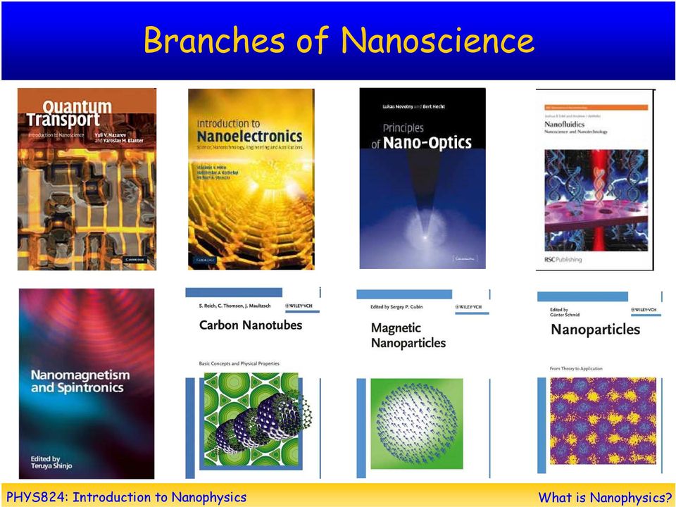
4 Branches of Nanoscience
5 Why are Nanostructures Interesting for Basic Research? Enhanced role of surface atoms with their unpaired spins and uncompensated bonds Reduced dimensionality at the nanoscale = strogly modified Density of States, enhanced Coulomb interaction, Quantum confinement effects = discrete energy levels quantum coherent effects in transport = quantum transport Semiclassical vs. Quantum Transport of (quasi)electrons

6 Limits of Top-Down Fabrication in Applied Physics and Electrical Engineering

7 Fundamental Quantum Effects Acting Against Moore s Law Nonscaling effects at nanometer MOSFETs: PRL 98, (2007) quantum tunneling of carriers through the gate insulator and through the body-to-drain junction dependence of sub-threshold behavior on temperature discrete doping effects power dissipated in various leakage mechanisms

8 Nanostructures: Bottom-Up Approach Fuhrer Lab, College Park Avouris Lab, IBM

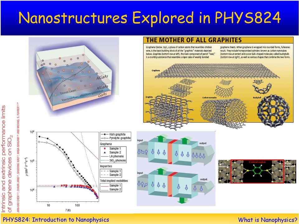
9 Nanostructures Explored in PHYS824
10 Experimental Tools of Nanoscience: STM and AFM

11 STM Images Fe on Cu(111) PRB 79, (2009) IBM, Almaden
 IBM,")
12 AFM Images Dai Lab, Science 319, 1229 (2008): Graphene Nanoribbons with ultrasmooth edges Kouwenhoven Lab: Double quantum dot integrated with quantum point contacts on both sides for spin qubit experiments

13 Equilibrium Nanophysics: Electronic Structure and Density of States 3 Density of States 1 0 3t holes 2t 1t 0 1t 2t Energy electrons 3t 0 h) k x (1/d a ) Local DOS at E F = DOS Fermi Energy E F Transverse Lattice Site

14 Nonequilibrium Nanophysics: Quantum Transport Externally set energy scales: Internal energy scales:

15 van Wees et al., PRL 60, 848 (1988) Conductance Quantization Avouris Lab, PRB 78, (R) (2008)

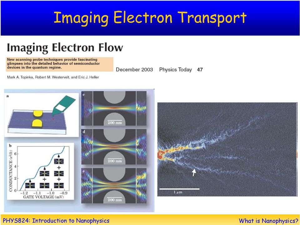
16 Imaging Electron Transport
17 Theory Quantum Hall Effect in 2DEG and Graphene

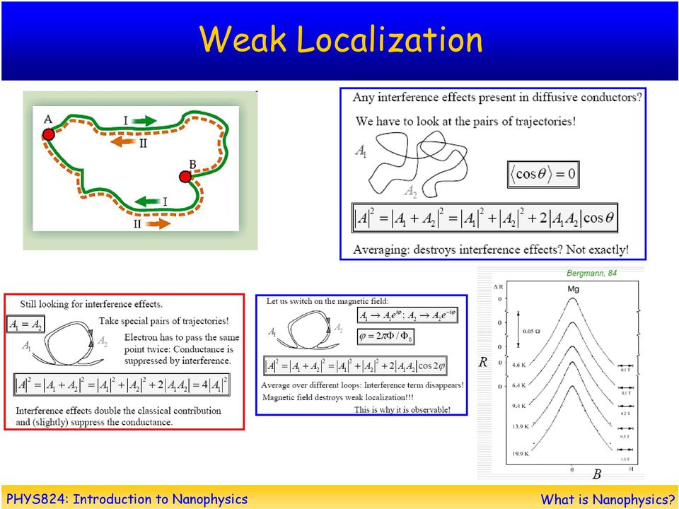
18 Weak Localization
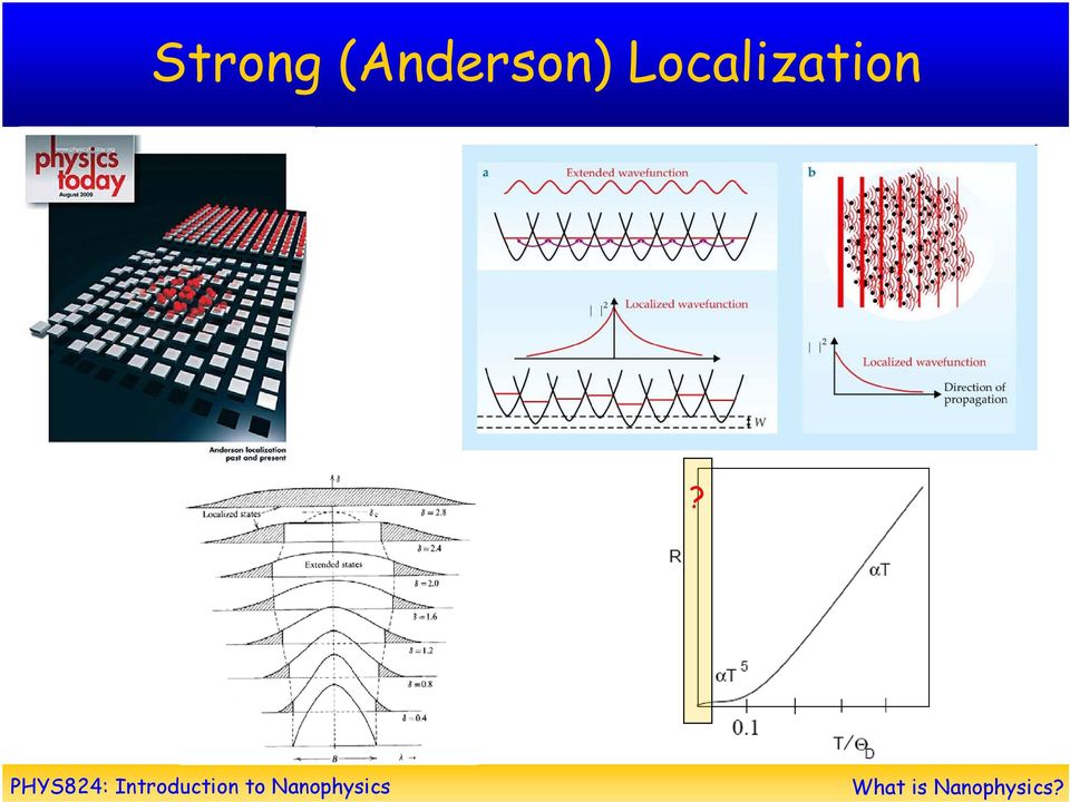
19 Strong (Anderson) Localization?
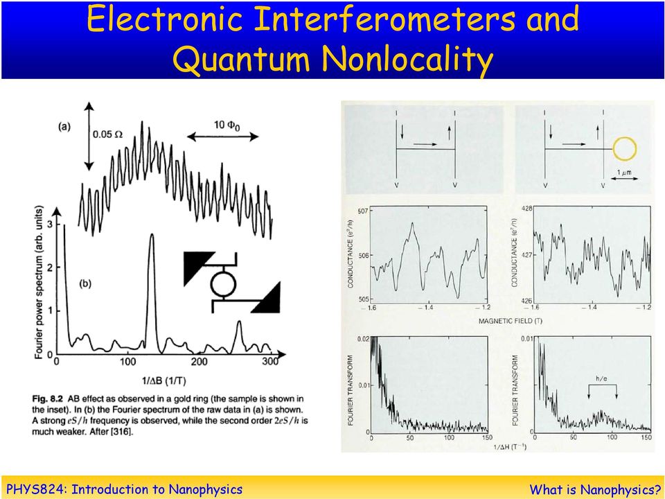
20 Electronic Interferometers and Quantum Nonlocality
21 Quantum Tunneling Esaki Diode (Nobel Prize 1973)
22 Coulomb Blockade Ensslin Lab, APL 92, (2008) H. van Houten, C. W. J. Beenakker, and A. A. M. Staring, cond-mat/
23 Nanophysics Applications: Spintronics (GMR, TMR, Spin-Torque)
24 Nanophysics Applications: Nanoelectronics with GNRs and CNTs
Nanocomputer & Architecture
 Nanocomputer & Architecture Yingjie Wei Western Michigan University Department of Computer Science CS 603 - Dr. Elise dedonckor Febrary 4 th, 2004 Nanocomputer Architecture Contents Overview of Nanotechnology
Experimental Observation of the Quantum Anomalous Hall Effect in a Magnetic Topological Insulator
 Experimental Observation of the Quantum Anomalous Hall Effect in a Magnetic Topological Insulator Chang et al., Science 340, 167 (2013). Joseph Hlevyack, Hu Jin, Mazin Khader, Edward Kim Outline: Introduction:
Nano Technology for Computer Science: Scope and Opportunities
 International Journal of Electronic and Electrical Engineering. ISSN 0974-2174, Volume 7, Number 3 (2014), pp. 213-218 International Research Publication House http://www.irphouse.com Nano Technology for
COURSE: PHYSICS DEGREE: COMPUTER ENGINEERING year: 1st SEMESTER: 1st
 COURSE: PHYSICS DEGREE: COMPUTER ENGINEERING year: 1st SEMESTER: 1st WEEKLY PROGRAMMING WEE K SESSI ON DESCRIPTION GROUPS GROUPS Special room for LECTU PRAC session RES TICAL (computer classroom, audiovisual
Nanoscience Course Descriptions
 Nanoscience Course Descriptions NANO*1000 Introduction to Nanoscience This course introduces students to the emerging field of nanoscience. Its representation in popular culture and journalism will be
Usage of Carbon Nanotubes in Scanning Probe Microscopes as Probe. Keywords: Carbon Nanotube, Scanning Probe Microscope
 International Journal of Arts and Sciences 3(1): 18-26 (2009) CD-ROM. ISSN: 1944-6934 InternationalJournal.org Usage of Carbon Nanotubes in Scanning Probe Microscopes as Probe Bedri Onur Kucukyildirim,
7/3/2014. Introduction to Atomic Force Microscope. Introduction to Scanning Force Microscope. Invention of Atomic Force Microscope (AFM)
") Introduction to Atomic Force Microscope Introduction to Scanning Force Microscope Not that kind of atomic Tien Ming Chuang ( 莊 天 明 ) Institute of Physics, Academia Sinica Tien Ming Chuang ( 莊 天 明 ) Institute
Introduction to Atomic Force Microscope Introduction to Scanning Force Microscope Not that kind of atomic Tien Ming Chuang ( 莊 天 明 ) Institute of Physics, Academia Sinica Tien Ming Chuang ( 莊 天 明 ) Institute
www.keithley.com 1 st Edition Nanotechnology Measurement Handbook A Guide to Electrical Measurements for Nanoscience Applications
 www.keithley.com 1 st Edition Nanotechnology Measurement Handbook A Guide to Electrical Measurements for Nanoscience Applications To get a free electronic version of this book, visit Keithley s Knowledge
Nanoelectronics 09. Atsufumi Hirohata Department of Electronics. Quick Review over the Last Lecture
 Nanoelectronics 09 Atsufumi Hirohata Department of Electronics 12:00 Wednesday, 4/February/2015 (P/L 006) Quick Review over the Last Lecture ( Field effect transistor (FET) ): ( Drain ) current increases
PPHY538M - 6 ECTS Formation expérimentale. Research training Chantal Tardif (CEA), Philippe Peyla (UJF) 3x5 days spent in a lab (3 different labs)
, Philippe Peyla (UJF) 3x5 days spent in a lab (3 different labs)") Nanochemistry and Nanoobjects Cyrille Train ([email protected]) SEMESTRE 3 SEMESTER 3 30 ECTS Cours obligatoires Compulsory courses 24 ECTS PCHI531B - 9 ECTS - Engineering of molecular assemblies,
Nanochemistry and Nanoobjects Cyrille Train ([email protected]) SEMESTRE 3 SEMESTER 3 30 ECTS Cours obligatoires Compulsory courses 24 ECTS PCHI531B - 9 ECTS - Engineering of molecular assemblies,
Solid-State Physics: The Theory of Semiconductors (Ch. 10.6-10.8) SteveSekula, 30 March 2010 (created 29 March 2010)
 SteveSekula, 30 March 2010 (created 29 March 2010)") Modern Physics (PHY 3305) Lecture Notes Modern Physics (PHY 3305) Lecture Notes Solid-State Physics: The Theory of Semiconductors (Ch. 10.6-10.8) SteveSekula, 30 March 2010 (created 29 March 2010) Review
Modern Physics (PHY 3305) Lecture Notes Modern Physics (PHY 3305) Lecture Notes Solid-State Physics: The Theory of Semiconductors (Ch. 10.6-10.8) SteveSekula, 30 March 2010 (created 29 March 2010) Review
Highlights of Solid State Physics. Man of the Year Nobel Prizes
 Highlights of Solid State Physics Man of the Year Nobel Prizes Silicon Technology Moore s Law Gordon Moore Intel Jack Kilby 14 nm 2014 Physics Nobel Prize 2000 Integrated Circuit Electrons in the Conduction
Theory and Modeling in Nanoscience
 Theory and Modeling in Nanoscience Report of the May 10 11, 2002, Workshop Conducted by the Basic Energy Sciences and Advanced Scientific Computing Advisory Committees to the Office of Science, Department
Quantised electrical conductance
 Quantised electrical conductance When the electronic mean free path λ of a wire is larger than the wire s length L, the wire behaves like an electron wave-guide and each wave-guide mode -or conduction
Introduction to Nanotechnology - History, Definition, Methodology, Applications, and Challenges. Instructor: Dr. Yu-Bin Chen Date: 07/25/2012
 Introduction to Nanotechnology - History, Definition, Methodology, Applications, and Challenges Instructor: Dr. Yu-Bin Chen Date: 07/25/2012 Outline Outline History Definition Methodology Applications
GRAPHENE: A NEW STAR IN MATERIAL SCIENCE
 GRAPHENE: A NEW STAR IN MATERIAL SCIENCE S. Sahoo 1 & A. K. Dutta 2 Department of Physics, National Institute of Technology Durgapur-713209, West Bengal, India. 1 E-mail: [email protected] 2 E-mail:
NANOSCALE SCIENCE AND ENGINEERING: MATERIALS, ELECTRONICS, PHOTONICS, BIOSENSORS AND BEYOND
 Inversion mode MOSFET p- pn junction Silicon film (n- type) Gate Silicon film (p- type) Gate oxide Continuing Education Program (CEP) on NANOSCALE SCIENCE AND ENGINEERING: MATERIALS, ELECTRONICS, PHOTONICS,
- particle with kinetic energy E strikes a barrier with height U 0 > E and width L. - classically the particle cannot overcome the barrier
 Tunnel Effect: - particle with kinetic energy E strikes a barrier with height U 0 > E and width L - classically the particle cannot overcome the barrier - quantum mechanically the particle can penetrated
CONTENTS. Preface. 1.1.2. Energy bands of a crystal (intuitive approach)
") CONTENTS Preface. Energy Band Theory.. Electron in a crystal... Two examples of electron behavior... Free electron...2. The particle-in-a-box approach..2. Energy bands of a crystal (intuitive approach)..3.
CONTENTS Preface. Energy Band Theory.. Electron in a crystal... Two examples of electron behavior... Free electron...2. The particle-in-a-box approach..2. Energy bands of a crystal (intuitive approach)..3.
Microscopie à force atomique: Le mode noncontact
 Microscopie à force atomique: Le mode noncontact Clemens Barth [email protected] CRMCN-CNRS, Campus de Lumny, Case 913, 13288 Marseille Cedex09, France La Londe les Maures (France) -- 20-21/03/2007
Nanotechnology and Its Impact on Modern Computer
 Global Journal of Researches in Engineering General Engineering Volume 12 Issue 4 Version 1.0 Year 2012 Type: Double Blind Peer Reviewed International Research Journal Publisher: Global Journals Inc. (USA)
Curriculum Vitae. Aykutlu Dâna. Date and place of birth: 2-12-1973 ISPARTA / TURKEY. Tel: 90 (536) 300 6515. Fax: 90 (312) 266 4579
 300 6515. Fax: 90 (312) 266 4579") Curriculum Vitae Aykutlu Dâna BIOGRAPHICAL Date and place of birth: 2-12-1973 ISPARTA / TURKEY CONTACT INFORMATION Present Affiliation: National Nanotechnology Research Center, Material Science and Nanotechnology
Curriculum Vitae Aykutlu Dâna BIOGRAPHICAL Date and place of birth: 2-12-1973 ISPARTA / TURKEY CONTACT INFORMATION Present Affiliation: National Nanotechnology Research Center, Material Science and Nanotechnology
Modification of Graphene Films by Laser-Generated High Energy Particles
 Modification of Graphene Films by Laser-Generated High Energy Particles Elena Stolyarova (Polyakova), Ph.D. ATF Program Advisory and ATF Users Meeting April 2-3, 2009, Berkner Hall, Room B, BNL Department
QUANTUM ENIGMA Summer 2014 Ted McIrvine
 QUANTUM ENIGMA Summer 2014 Ted McIrvine June 17: Once Over Lightly & Newtonian Mechanics June 24: Electricity, Magnetism, Light & the Puzzles of 1900 July 1: Atomic Theory, Quantum Theory, Paradoxes and
The 2007 Nobel Prize in Physics. Albert Fert and Peter Grünberg
 The 2007 Nobel Prize in Physics Albert Fert and Peter Grünberg Albert Fert and Peter Grünberg are well-known for having opened a new route in science and technology by their discovery of the Giant MagnetoResistance
Atomic Force Microscopy. July, 2011 R. C. Decker and S. Qazi
 Atomic Force Microscopy July, 2011 R. C. Decker and S. Qazi Learning through Visualization Visualization of physical phenomena can confirm hypothesis Observation provides opportunities for study without
Nanotechnology Integration to enhance Undergraduate Engineering Education
 Nanotechnology Integration to enhance Undergraduate Engineering Education Nael Barakat, Ph.D. P.Eng. FASME Associate Professor Mechanical Engineering Program Chair School of Engineering, Grand Valley State
Graphene a material for the future
 Graphene a material for the future by Olav Thorsen What is graphene? What is graphene? Simply put, it is a thin layer of pure carbon What is graphene? Simply put, it is a thin layer of pure carbon It has
Quantum control of individual electron and nuclear spins in diamond lattice
 Quantum control of individual electron and nuclear spins in diamond lattice Mikhail Lukin Physics Department, Harvard University Collaborators: L.Childress, M.Gurudev Dutt, J.Taylor, D.Chang, L.Jiang,A.Zibrov
Lecture 6 Scanning Tunneling Microscopy (STM) General components of STM; Tunneling current; Feedback system; Tip --- the probe.
 General components of STM; Tunneling current; Feedback system; Tip --- the probe.") Lecture 6 Scanning Tunneling Microscopy (STM) General components of STM; Tunneling current; Feedback system; Tip --- the probe. Brief Overview of STM Inventors of STM The Nobel Prize in Physics 1986 Nobel
Lecture 6 Scanning Tunneling Microscopy (STM) General components of STM; Tunneling current; Feedback system; Tip --- the probe. Brief Overview of STM Inventors of STM The Nobel Prize in Physics 1986 Nobel
XCVII Congresso Nazionale
 XCVII Congresso Nazionale The Fe(001)-p(1x1)O surface: scanning tunneling microscopy (STM) results and related issues Lamberto Duò CNISM - Dipartimento di Fisica Politecnico di Milano Oxides and thin (few
NANOTECHNOLOGY BACKGROUND
 NANOTECHNOLOGY BACKGROUND Introduction and Overview Nanotechnology is defined as the study of the fundamental laws and theories of atoms and structures that have critical dimensions between 1 and 100 nanometers.
Matter, Materials, Crystal Structure and Bonding. Chris J. Pickard
 Matter, Materials, Crystal Structure and Bonding Chris J. Pickard Why should a theorist care? Where the atoms are determines what they do Where the atoms can be determines what we can do Overview of Structure
X-Rays and Magnetism From Fundamentals to Nanoscale Dynamics
 X-Rays and Magnetism From Fundamentals to Nanoscale Dynamics Joachim Stöhr Stanford Synchrotron Radiation Laboratory X-rays have come a long way 1895 1993 10 cm 10 µm 100 nm Collaborators: SSRL Stanford:
CARBON NANOTUBE NANOELECTROMECHANICAL SYSTEMS
 CARBON NANOTUBE NANOELECTROMECHANICAL SYSTEMS PHD THESIS BY MARIANNA SLEDZINSKA Director: Prof. Adrian Bachtold Tutor de la UAB: Prof. Javier Rodriguez Dr. Adrian Bachtold, profesor del CSIC en el CIN2,
Spin-flip excitation spectroscopy with STM excitation of allowed transition adds an inelastic contribution (group of Andreas Heinrich, IBM Almaden)
") Magnetism at the atomic scale by Scanning Probe Techniques Kirsten von Bergmann Institute of Applied Physics Magnetism with SPM Spin-polarized scanning tunneling microscopy SP-STM density of states of
Magnetism at the atomic scale by Scanning Probe Techniques Kirsten von Bergmann Institute of Applied Physics Magnetism with SPM Spin-polarized scanning tunneling microscopy SP-STM density of states of
Hard Condensed Matter WZI
 Hard Condensed Matter WZI Tom Gregorkiewicz University of Amsterdam VU-LaserLab Dec 10, 2015 Hard Condensed Matter Cluster Quantum Matter Optoelectronic Materials Quantum Matter Amsterdam Mark Golden Anne
Crystalline solids. A solid crystal consists of different atoms arranged in a periodic structure.
 Crystalline solids A solid crystal consists of different atoms arranged in a periodic structure. Crystals can be formed via various bonding mechanisms: Ionic bonding Covalent bonding Metallic bonding Van
Thermal unobtainiums? The perfect thermal conductor and the perfect thermal insulator
 Thermal unobtainiums? The perfect thermal conductor and the perfect thermal insulator David G. Cahill Materials Research Lab and Department of Materials Science and Engineering, U. of Illinois Gratefully
Free Electron Fermi Gas (Kittel Ch. 6)
") Free Electron Fermi Gas (Kittel Ch. 6) Role of Electrons in Solids Electrons are responsible for binding of crystals -- they are the glue that hold the nuclei together Types of binding (see next slide)
Free Electron Fermi Gas (Kittel Ch. 6) Role of Electrons in Solids Electrons are responsible for binding of crystals -- they are the glue that hold the nuclei together Types of binding (see next slide)
Ph.D Brochure Department of Physics
 Ph.D Brochure Department of Physics Year 2016 Introduction High Energy Physics Optics, Spectroscopy and Laser-Plasma Physics Computational Condensed Matter Physics Experimental Condensed Matter Physics
Laser Based Micro and Nanoscale Manufacturing and Materials Processing
 Laser Based Micro and Nanoscale Manufacturing and Materials Processing Faculty: Prof. Xianfan Xu Email: [email protected] Phone: (765) 494-5639 http://widget.ecn.purdue.edu/~xxu Research Areas: Development
Solid State Electronics and Photonics Electrical and Computer Engineering The Ohio State University
 Solid State Electronics and Photonics Electrical and Computer Engineering The Ohio State University An Overview for Prospective Students http://www.ece.osu.edu/ssep SSEP Area: Who Are We? First Row Betty
Sub-gap conductance fluctuations in superconductor-graphene hybrid nanostructures
 Sub-gap conductance fluctuations in superconductor-graphene hybrid nanostructures G.Albert, B.Kaviraj, F.Gustavo, F.Lefloch, L.Jansen Laboratoire de Transport Electronique Quantique et Supraconductivité
nanohub.org Toward On-Line Simulation for Materials and Nanodevices by Design
 Univ. of Florida, Univ. of Illinois, Morgan State Univ., Northwestern Univ. Purdue Univ. Stanford Univ., UTEP nanohub.org Toward On-Line Simulation for Materials and Nanodevices by Design 1 Gerhard Klimeck,
Subject Area(s) Biology. Associated Unit Engineering Nature: DNA Visualization and Manipulation. Associated Lesson Imaging the DNA Structure
 Biology. Associated Unit Engineering Nature: DNA Visualization and Manipulation. Associated Lesson Imaging the DNA Structure") Subject Area(s) Biology Associated Unit Engineering Nature: DNA Visualization and Manipulation Associated Lesson Imaging the DNA Structure Activity Title Inside the DNA Header Image 1 ADA Description:
Subject Area(s) Biology Associated Unit Engineering Nature: DNA Visualization and Manipulation Associated Lesson Imaging the DNA Structure Activity Title Inside the DNA Header Image 1 ADA Description:
Technology White Papers nr. 13 Paul Holister Cristina Román Vas Tim Harper
 QUANTUM DOTS Technology White Papers nr. 13 Paul Holister Cristina Román Vas Tim Harper QUANTUM DOTS Technology White Papers nr. 13 Release Date: Published by Científica Científica, Ltd. www.cientifica.com
Quantum Computing for Beginners: Building Qubits
 Quantum Computing for Beginners: Building Qubits Suzanne Gildert Condensed Matter Physics Research (Quantum Devices Group) University of Birmingham 28/03/2007 Overview of this presentation What is a Qubit?
Scanning Tunneling Microscopy: Fundamentals and Applications
 McGill University, Montreal, March 30 th 2007 Scanning Tunneling Microscopy: Fundamentals and Applications Federico Rosei Canada Research Chair in Nanostructured Organic and Inorganic Materials Énergie,
Fundamental Nanomaterials Research and Development: An Australian Perspective
 Fundamental Research and Development: An Australian Perspective Professor Max Lu FTSE, Fed Fellow, Director Http://www.arccfn.org.au Gross Domestic Expenditure on R&D Australia 10000 8000 Business Government
From Nano-Electronics and Photonics to Renewable Energy
 From Nano-Electronics and Photonics to Renewable Energy Tom Smy Department of Electronics, Carleton University Questions are welcome! OUTLINE Introduction: to EE and Engineering Physics Renewable Energy
Università degli Studi di Padova Dipartimento di Fisica e Astronomia Corso di Laurea Magistrale in Fisica
 Università degli Studi di Padova Dipartimento di Fisica e Astronomia Corso di Laurea Magistrale in Fisica SCANNING PROBE MICROSCOPY OF GRAPHENE AND SELF-ASSEMBLED MOLECULES Nicola Galvanetto ANNO ACCADEMICO
The Raman Fingerprint of Graphene
 The Raman Fingerprint of Graphene A. C. Ferrari 1, J. C. Meyer 2, V. Scardaci 1, C. Casiraghi 1, M. Lazzeri 3, F. Mauri 3, S. Piscanec 1, D. Jiang 4, K. S. Novoselov 4, S. Roth 2, A. K. Geim 4 1 Department
PHYSICS OF NANOSTRUCTURES
 MOSCOW INSTITUTE OF PHYSICS AND TECHNOLOGY (STATE UNIVERSITY) INTERNATIONAL MASTER S DEGREE PROGRAMMES PHYSICS OF NANOSTRUCTURES About The programme provides students with knowledge of the latest fundamental
SPM 150 Aarhus with KolibriSensor
 Customied Systems and Solutions Nanostructures and Thin Film Deposition Surface Analysis and Preparation Components Surface Science Applications SPM 150 Aarhus with KolibriSensor Atomic resolution NC-AFM
Electronic transport properties of nano-scale Si films: an ab initio study
 Electronic transport properties of nano-scale Si films: an ab initio study Jesse Maassen, Youqi Ke, Ferdows Zahid and Hong Guo Department of Physics, McGill University, Montreal, Canada Motivation (of
Tutorial on Electronic Transport. Jesper Nygård Niels Bohr Institute University of Copenhagen
 Tutorial on Electronic Transport Jesper Nygård Niels Bohr Institute University of Copenhagen ...for newcomers in the field... Prior knowledge: What is a carbon nanotube (Some) nanotube band structure Ohm
New magnetism of 3d monolayers grown with oxygen surfactant: Experiment vs. ab initio calculations
 New magnetism of 3d monolayers grown with oxygen surfactant: Experiment vs. ab initio calculations 1. Growth and structure 2. Magnetism and MAE 3. Induced magnetism at oxygen Klaus Baberschke Institut
1 Introduction. 1.1 Historical Perspective
 j1 1 Introduction 1.1 Historical Perspective The invention of scanning probe microscopy is considered one of the major advances in materials science since 1950 [1, 2]. Scanning probe microscopy includes
Fluid transport at the nano- and meso- scales
 NanoSOFT Fluid transport at the nano- and meso- scales from fundamentals to applications in energy harvesting and desalination process Alessandro Siria Starting Grant 2014 Panel: PE 3, Condensed Matter
Explain the ionic bonds, covalent bonds and metallic bonds and give one example for each type of bonds.
 Problem 1 Explain the ionic bonds, covalent bonds and metallic bonds and give one example for each type of bonds. Ionic Bonds Two neutral atoms close to each can undergo an ionization process in order
Fluids Confined in Carbon Nanotubes
 Fluids Confined in Carbon Nanotubes Constantine M. Megaridis Micro/Nanoscale Fluid Transport Laboratory Mechanical and Industrial Engineering University of Illinois at Chicago 1 Background and Societal
Predicted Performance Advantages of Carbon Nanotube Transistors with Doped Nanotubes as Source/Drain
 Predicted Performance Advantages of Carbon Nanotube Transistors with Doped Nanotubes as Source/Drain Jing Guo, Ali Javey, Hongjie Dai, Supriyo Datta and Mark Lundstrom School of ECE, Purdue University,
Single Defect Center Scanning Near-Field Optical Microscopy on Graphene
 1 2 3 4 5 6 7 8 9 10 11 12 13 14 15 16 17 Single Defect Center Scanning Near-Field Optical Microscopy on Graphene J. Tisler, T. Oeckinghaus, R. Stöhr, R. Kolesov, F. Reinhard and J. Wrachtrup 3. Institute
Unit 12 Practice Test
 Name: Class: Date: ID: A Unit 12 Practice Test Multiple Choice Identify the choice that best completes the statement or answers the question. 1) A solid has a very high melting point, great hardness, and
UNIT I: INTRFERENCE & DIFFRACTION Div. B Div. D Div. F INTRFERENCE
 107002: EngineeringPhysics Teaching Scheme: Lectures: 4 Hrs/week Practicals-2 Hrs./week T.W.-25 marks Examination Scheme: Paper-50 marks (2 hrs) Online -50marks Prerequisite: Basics till 12 th Standard
Chapter 4 Information and Communication Technologies (ICT)
") NANOYOU Teachers Training Kit in Nanotechnologies Chapter 4 Information and Communication Technologies (ICT) MODULE 2- Applications of Nanotechnologies Written by Luisa Filipponi and Duncan Sutherland
NANOYOU Teachers Training Kit in Nanotechnologies Chapter 4 Information and Communication Technologies (ICT) MODULE 2- Applications of Nanotechnologies Written by Luisa Filipponi and Duncan Sutherland
CHEMICAL SCIENCES REQUIREMENTS [61-71 UNITS]
![CHEMICAL SCIENCES REQUIREMENTS [61-71 UNITS]](/thumbs/39/18644108.jpg "CHEMICAL SCIENCES REQUIREMENTS [61-71 UNITS]") Chemical Sciences Major Chemistry is often known as the central science because of the key position it occupies in modern science and engineering. Most phenomena in the biological and Earth sciences can
Chemical Sciences Major Chemistry is often known as the central science because of the key position it occupies in modern science and engineering. Most phenomena in the biological and Earth sciences can
Ultra-High Density Phase-Change Storage and Memory
 Ultra-High Density Phase-Change Storage and Memory by Egill Skúlason Heated AFM Probe used to Change the Phase Presentation for Oral Examination 30 th of May 2006 Modern Physics, DTU Phase-Change Material
The Early History of Nanotechnology
 OpenStax-CNX module: m14504 1 The Early History of Nanotechnology Devon Fanfair Salil Desai Christopher Kelty This work is produced by OpenStax-CNX and licensed under the Creative Commons Attribution License
Magnetic dynamics driven by spin current
 Magnetic dynamics driven by spin current Sergej O. Demokritov University of Muenster, Germany Giant magnetoresistance Spin current Group of NonLinear Magnetic Dynamics Charge current vs spin current Electron:
Theoretical investigation on armchair graphene nanoribbons. with oxygen-terminated edges
 Theoretical investigation on armchair graphene nanoribbons with oxygen-terminated edges Hongyu Ge, Guo Wang* and Yi Liao Department of Chemistry, Capital Normal University, Beijing 100048, China * Corresponding
Tobias Märkl. November 16, 2009
 ,, Tobias Märkl to 1/f November 16, 2009 1 / 33 Content 1 duction to of Statistical Comparison to Other Types of Noise of of 2 Random duction to Random General of, to 1/f 3 4 2 / 33 , to 1/f 3 / 33 What
NMR SPECTROSCOPY. Basic Principles, Concepts, and Applications in Chemistry. Harald Günther University of Siegen, Siegen, Germany.
 NMR SPECTROSCOPY Basic Principles, Concepts, and Applications in Chemistry Harald Günther University of Siegen, Siegen, Germany Second Edition Translated by Harald Günther JOHN WILEY & SONS Chichester
Lecture 4 Scanning Probe Microscopy (SPM)
") Lecture 4 Scanning Probe Microscopy (SPM) General components of SPM; Tip --- the probe; Cantilever --- the indicator of the tip; Tip-sample interaction --- the feedback system; Scanner --- piezoelectric
Lecture 4 Scanning Probe Microscopy (SPM) General components of SPM; Tip --- the probe; Cantilever --- the indicator of the tip; Tip-sample interaction --- the feedback system; Scanner --- piezoelectric
The Application of Density Functional Theory in Materials Science
 The Application of Density Functional Theory in Materials Science Slide 1 Outline Atomistic Modelling Group at MUL Density Functional Theory Numerical Details HPC Cluster at the MU Leoben Applications
Quantum Systems for Information Technology
 Lecture Quantum Systems for Information Technology fall term (HS) 2010 Lecturer: e Andreas Wallraff office: HPF D 8/9, ETH Hoenggerberg email: [email protected] What is this lecture about? Quantum
Atomic Force Microscopy. Long Phan Nanotechnology Summer Series May 15, 2013
 Atomic Force Microscopy Long Phan Nanotechnology Summer Series May 15, 2013 1 World s Smallest Movie 2 Outline What is AFM? How does AFM Work? 3 Modes: Contact mode Non contact mode Tapping mode Imaging
Computational Nanoscience of Soft Matter
 ChE/MSE 557 Computational Nanoscience of Soft Matter Fall 2006 Instructor: Professor Sharon C. Glotzer Class meets: Tues 3:00-6:00 Location: Room 3336 BD, Duderstadt Center Room 3336 AC, Duderstadt Center
SEMICONDUCTOR I: Doping, semiconductor statistics (REF: Sze, McKelvey, and Kittel)
") SEMICONDUCTOR I: Doping, semiconductor statistics (REF: Sze, McKelvey, and Kittel) Introduction Based on known band structures of Si, Ge, and GaAs, we will begin to focus on specific properties of semiconductors,
SEMICONDUCTOR I: Doping, semiconductor statistics (REF: Sze, McKelvey, and Kittel) Introduction Based on known band structures of Si, Ge, and GaAs, we will begin to focus on specific properties of semiconductors,
Introduction to CMOS VLSI Design
 Introduction to CMOS VLSI esign Slides adapted from: N. Weste,. Harris, CMOS VLSI esign, Addison-Wesley, 3/e, 24 Introduction Integrated Circuits: many transistors on one chip Very Large Scale Integration
PHYSICAL METHODS, INSTRUMENTS AND MEASUREMENTS Vol. IV Femtosecond Measurements Combined With Near-Field Optical Microscopy - Artyom A.
 FEMTOSECOND MEASUREMENTS COMBINED WITH NEAR FIELD OPTICAL MICROSCOPY Artyom A. Astafiev, Semyonov Institute of Chemical Physics, Moscow, Russian Federation. Keywords: diffraction limit nearfield scanning
High Open Circuit Voltage of MQW Amorphous Silicon Photovoltaic Structures
 High Open Circuit Voltage of MQW Amorphous Silicon Photovoltaic Structures ARGYRIOS C. VARONIDES Physics and EE Department University of Scranton 800 Linden Street, Scranton PA, 18510 United States Abstract:
Chemical Synthesis. Overview. Chemical Synthesis of Nanocrystals. Self-Assembly of Nanocrystals. Example: Cu 146 Se 73 (PPh 3 ) 30
 30") Chemical Synthesis Spontaneous organization of molecules into stable, structurally well-defined aggregates at the nanometer length scale. Overview The 1-100 nm nanoscale length is in between traditional
Chemical Synthesis Spontaneous organization of molecules into stable, structurally well-defined aggregates at the nanometer length scale. Overview The 1-100 nm nanoscale length is in between traditional
The Future of Data Storage
 The Future of Data Storage Principles, Potential and Problems Hans Coufal IBM Almaden Research Center Areal Density Megabits/in2 arpers2001ab2.prz 1E+6 10 6 1E+5 10 5 1E+4 10 4 1E+3 10 3 1E+2 10 2 1E+1
Nano-Microscopy: Lecture 1. Pavel Zinin HIGP, University of Hawaii, Honolulu, USA
 GG 711: Advanced Techniques in Geophysics and Materials Science Nano-Microscopy: Lecture 1 Scanning Tunneling and Atomic Force Microscopies Principles Pavel Zinin HIGP, University of Hawaii, Honolulu,
SUPERCONDUCTIVITY. PH 318- Introduction to superconductors 1
 SUPERCONDUCTIVITY property of complete disappearance of electrical resistance in solids when they are cooled below a characteristic temperature. This temperature is called transition temperature or critical