Chapter 6 TRANSISTOR-TRANSISTOR LOGIC. 3-emitter transistor.
|
|
|
- Flora Porter
- 9 years ago
- Views:
Transcription
1 Chapter 6 TRANSISTOR-TRANSISTOR LOGIC The evolution from DTL to TTL can be seen by observing the placement of p-n junctions. For example, the diode D2 from Figure 2 in the chapter on DTL can be replaced by a transistor whose collector is pulled up to the power supply; transistor Q 2 in Figure 1 below. The p-n junction of D2 is replaced by the BE junction of Q2 and with the current gain of the transistor, the current going into the base of Q3 is greatly increased, increasing the fanout. Figure 1. TTL Gate. Figure 2. Configuration of Q 1 as a 3-emitter transistor. The input diodes and D1 are replaced by the multi-emitter NPN transistor, Q1, in Fig. 1 and represented by the drawing in Figure 2. Later on, we will make additional modifications to this curcuit to improve its performance further. The analysis of this circuit follows very much the same path as the analysis of the DTL gate. For the most part, we will consider the input transistor, Q1, to act just like two diodes. The transistor Q2, however, will operate in all three regions. The treatment of the output voltages and currents will be treated the same as the DTL gate and Q3 will either be cutoff or saturated, corresponding to an output high and an output low, respectively. ANALYSIS WITH ONE OR MORE INPUTS LOW With an input low, Q3 should be cutoff. We will assume Q2 is cutoff and then check our assumption. If Q2 is cutoff, then there can be no current coming out of the collector of Q1, hence its base-collector junction can be modeled as an open circuit. The base-emitter junction of Q1 will be conducting. The circuit with these models substituted for the transistors is shown in Figure 3. Note the similarity to the DTL circuit under the same conditions. The two unused inputs are assumed to be high, and are thus, modeled as open. From this case, we can see that V oh = 5 volts with no load, and I inl = -I 1 = -(5-0.9)/4K = ma Transistor-Transistor Logic 1

2 Figure 3. TTL circuit model with one input low. We turn now to finding V InLmax. We will use the criterion that V in will be considered as a low as long as Q3 is kept cutoff. If the base voltage for Q3 can be raised to 0.5 Volts without turning it on, then there will be 0.5 ma current in the 1KΩ resistor. This current can only come from Q2, which means it must be conducting. Even assuming all this 0.5 ma comes through the collector of Q2, the voltage drop across the 1.4 KΩ resistor will be 0.7 Volts, not enough to cause the transistor to saturate. Thus, the active model for Q2 is appropriate as shown in Figure 4. Figure 4. TTL circuit model to determine V inlmax. If we assume that β=30, the base current in Q2 is 05. ma 05. IB2 = β + 1 = 31 = mA Because this current is coming out of the collector of Q1, the base- collector junction of Q1 is on, and is modeled as a diode in Figure 4. The voltage at B1, the base of Q1, is V B1 = = 1.9 Volts The current coming down through the 4 KΩ resistor, I 1, is I1 = = mA 4K This is considerably more than is going into the base of Q2, therefore, the input BE junction of Q1 will also still be conducting. The maximum voltage at the input is V inlmax = = 1.2 Volts Transistor-Transistor Logic 2

3 CALCULATIONS WITH INPUT HIGH The circuit model for the TTL gate with all inputs high is shown in Figure 5. Both Q2 and Q3 are modeled as saturated, an assumption that must be verified. With the inputs high, Q1 is modeled as two diodes with the B-E diodes cutoff, and B-C diode conducting. Figure 5. TTL gate circuit model with all inputs high. The voltage at the base of Q1 is V B1 = = 2.3 Volts. The current down through the 4 KΩ resistor, I 1 is I = = mA 4K All this current goes into the base of Q2. I B2 = ma If Q2 is saturated, voltage at its collector terminal is V C2 = = 1.0 Volts And the collector current is I C2 = I = = mA 14. K Clearly, if β = 30, βι B2 > I C2, and, therefore, Q2 is saturated. The current coming out of the emitter of Q2 is the sum of the base and collector currents. Part of this current will go down through the 1 KΩ resistor to ground and the rest will enter the base of Q3. I B3 = I B2 + I C2 - I 3 = = ma Transistor-Transistor Logic 3

4 The maximum collector current that Q 3 can carry and still be in saturation is βi B3 =81.96 ma, assuming β=30. The maximum current the gate can sink when the output is low I olmax = I Csatmax - I 4 = = ma Now let's turn our attention back to the input and determine V inhmin and I inh. We will define the input voltage to be high as long as no current goes out the input terminal. Thus, all we have to do is keep the input voltage high enough so that the B-E p-n junction of Q1 does not turn on. Thus, V inhmin = = 1.7 Volts CALCULATION OF I inh With the input voltage at a high, say 5 volts, the transistor Q1 will be operating in the reverse active mode. The B-E junction is reverse biased, and the B-C junction is forward biased with a base current of ma. If there were significant curent gain, you would expect to see a large current going into the input. However, the reverse β is typically on the order of Thus, I inh = β R I = = ma This current would add to the current going into the base of Q2, but is ignored because it is quite small and because β R is made as small as possible and this input current is a maximum and cannot be counted on. THE TOTEM POLE OUTPUT STAGE One of the problems with the TTL gate circuit we have been analyzing is that the pull-up resistor on the output transistor will prevent rapid charging of any wiring capacitance on the output. One way to improve the rise time is to reduce the resistance value as is often done, but this also increases the power dissipation when the output is low. If we look at the circuit, we observe that when the transistor is saturated, it presents a very low effective resistance to ground. The problem arises when the output is high and the pull-up resistor is too large. Ideally we would like to have a very low resistance pull-up when the output is high, but a very high pull-up resistance when the output is low. In this way, we could get quick charging and very low power dissipation. The totem-pole output stage for TTL, shown in Figure 6, does just that. Figure 6. TTL gate with totem-pole output. Transistor-Transistor Logic 4

5 This circuit operates just like the original circuit except that Q 4 is on when the output is high and off when the output is low. We need to verify this operation. OUTPUT LOW Figure 7 shows the TTL circuit with all inputs high and the output low. The models for the transistors are shown as before, except diode D and transistor Q 4 are added and shown as cutoff. Figure 7. TTL gate with totem-pole output circuit model with inputs high. The analysis of this circuit proceeds exactly the same as before. The currents, I 1, I 2, I 3, and I B3 are the same as before. With the diode and Q 4 not conducting, I olmax is now the same as I C4max, ma. We only need to show that the diode D and transistor Q 4 are indeed off. The voltage at the bottom of the diode is 0.2 Volts and the voltage at the base of Q 4 equal to the voltage at the collector of Q 2 ; V C2 = ( ) = 1.0 Volts. Thus, the voltage across the B-E junction of Q 4 plus the diode is 0.8 Volts. If one conducts, the other must also. To take both out of cutoff would require at least = 1.1 Volts. Thus, both are off. OUTPUT HIGH This condition occurs when one or more inputs are low. The circuit is shown in Figure 8 with the appropriate models used for the transistors and the diode. In this case, Q2 and Q3 are both cutoff while Q4 and the diode are conducting. We have to assume here that there is some load and that the output current is not zero. Transistor-Transistor Logic 5

6 Figure 8. TTL totem-pole circuit model with output high. The current coming out the output terminal I S (=-I o ) is the sum of the currents coming down through the base and the collector. Thus, I S = I B4 + βi B4 Because each TTL load represents 13 µa, if we assume there are 10 loads, then I S = 130 µa. The base current is I B4 130µ A = 1+ β = 42. µ A where we have assumed a β of 30. Then taking the path down through the 1.4 KΩ resistor to the output. the output voltage is V o = µΑ 1.4K = 3.6 Volts The voltage drop across the 1.4 KΩ resistor is neglegible. Of course as the current increases, the output voltage will drop further. TERMINAL SPECIFICATIONS OF THE TTL GATE We are now ready to make the table showing the terminal specifications for the TTL gate. These are shown in Table Table 1. Terminal Specifications For TTL V inlmax = 1.2 V V ol = 0.2 V inhmin = 1.7 I inl = ma I inh = 13 µa V oh = 3.4 (@I o = -130 µa) I olmax = ma I oh = undetermined Transistor-Transistor Logic 6

7 Figure 9. Data for 00, 04, 10, and 30 NAND gates for several TTL families (Abstracted from Texas Instruments TTL Data Book.) Transistor-Transistor Logic 7

8 MANUFACTURER S DATA SHEETS The terminal specifications of several TTL families are shown in Figure 9. You will note the values given for various voltages and currents are quite different from those we calculated. This difference comes from the fact that manufacturing tolerances and variations cannot be closely controlled, hence, the specifications given by the manufacturers are much more conservative than our calculations which were based on nominal values. Also note that the limits are usually given as a maximum or a minimum, depending on which limit is normally used in design. For example, I inlmax is given as -1.6 ma for the 74xx series. What this means is that as a designer, your driver must be able to sink as much as 1.6 ma when the input to the gate is pulled low. You will note that the TTL gate is rather loosely specified. The question invariably arises as to how one reads the data sheets or designs with this data. Figure 10 shows the allowed operating regions for a 7400, 2-input NAND gate. The best description of these operating regions is probably given by the following examples. Example 1: If the input voltage is between 0.00 and 0.08 volts, the output voltage will be below V CC and above 2.4 volts as shown in Figure 10a. Example 2: If the input voltage is between 2.00 and V CC, the input current will be between 0 and 40 µa as shown in Figure 10b. You will note in the above examples that there is no mathematical relationship between one variable and another. There is simply not enough data to develop one and the variability of the manufacturing process prohibits the manufacturer from providing one. In a design setting, you must stay within the limits provided by the manufacturer. For example, if you wanted to connect a resistor from the output of a 7400 gate and ground, what would be the limits allowed on the resistance value? Figure 10c provides part of the answer. If we assume that we must operate within the shaded region which represents a High level output, we should not allow the output to drop below 2.4 volts with 400 µa coming out of the gate. The minimum value would be 6 KΩ. The upper limit is, of course, infinite; an open circuit (V o = V CC, I o = 0). There are a few data points provide by the specifications that are not within the limits of normal operation. For example, if the input voltage drops below zero, it is allowed to drop to -1.5 volts where you may expect as much as 12 ma coming out of a 7400 gate input. Most of this current comes from an input clamp diode which has not been shown on our drawings. Transistor-Transistor Logic 8

9 Transistor-Transistor Logic 9
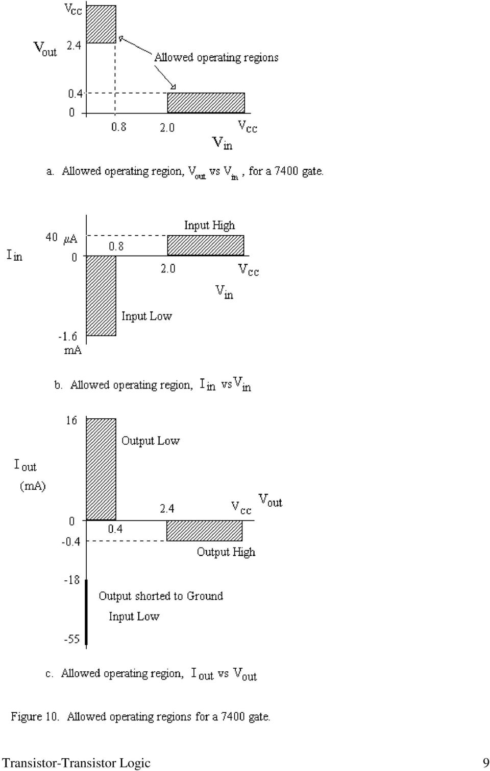
10 Another non-standard data point of interest is I os, the short-circuit output current. This is the current you get from the gate output if the output is shorted to ground when the output of the gate would otherwise be high. In this case, both minimum and maximum values are given, -18 to -55 ma. If you went to the laboratory and actually performed this deed, you could expect a current somewhere in this range. How does this affect the designer? For example, a designer might be tempted to connect the output of the 7400 gate directly to the base of an NPN transistor whose emitter is grounded. In this case, the "high" output voltage is clamped at 0.80 V by the BE junction. What current can you expect into the base of the transistor when the gate output goes "high"? This condition is tricky and perhaps open to some debate, but the conservative designer must recognize that the operation is between the short circuit case and the case where V ohmin =2.4V when I oh =- 400µA. The conservative designer would conclude that the current might be as low as 400 µa and as high as 55 ma; the worst cases. It is possible to go back to the circuit of the gate with 0.8 volts at the output terminal and calculate the current. However, this analysis would be for nominal values only and not provide definitive limits on the current. Note the notation at the bottom of the specification table in Figure 9. This notation discusses the limit on the amount of time a short circuit is allowed to be connected to the output of some gates. This time limit is based on the amount of time it takes the internal components of the integrated circuit to heat up to its maximum allowed value. While connecting a transistor base to the output is not exactly a short circuit, it is outside the allowed operating region and probably should have the same time limits as the short circuit. TERMINAL CHARACTERISTICS During the previous discussions on TTL, we were looking at circuit operation and developing an understanding of how the terminal specifications were arrived at. Let us now take a broader look at these characteristics. First, the input currents are quite high when the input is low, requiring the driver to sink a lot of current. When the input is high, the input current into the gate is quite low. Thus, any circuit which is supposed to drive the input to a TTL gate must concentrate on sinking current, and only needs to source a little current when the driver output voltage is high. Second, the output strength of the TTL gate matches the strength requirements at the input. An example is given in Figure 11. The TTL gate can sink a large current when its output is low, but can only source a small current when the output is high. Thus, if the TTL gate is expected to drive a circuit that is not another TTL circuit, you must exercise care when designing the interface. The load circuit must not require large input currents when its input is high, but may use larger currents when the input voltage is low. Transistor-Transistor Logic 10

11 Figure 11. When driving other TTL gates as loads, a 7400 gate must be able to sink more current than it needs to source. These requirements must be kept in mind when designing interfaces with the TTL gate at both the input and the output. Examples of interfacing with TTL gates are shown in Figure 12 and 13. See data books for more complete data. Transistor-Transistor Logic 11

12 Figure 12. Several ways to drive loads from TTL gates. Figure 13. Several interfaces to drive TTL gates. Transistor-Transistor Logic 12

13 WIRED-AND CONNECTION Because the active pull-up or totem-pole output of the TTL gate always has one transistor cutoff and the other turned on, you cannot connect two outputs together. If one is trying to pull the output high, and the other is trying to pull it low, you will have a very low impedance path to ground and very large currents. For the same reason, the output must not be connected to any voltage source or to ground through a low impedance path. In one state or the other, there would be a low impedance path and large currents. OPEN COLLECTOR GATES In order to overcome the limitations created by the totem pole output circuit, some gates are manufactured with the output collector left open. One example is the 7405, a quad 2- input NAND gate with open collector outputs. If you connect a resistor as the pull-up, you can use this resistor to source current when the output is high and/or you can wire- AND the collectors together. TTL FAMILIES As the designers of TTL gates became more sophisticated, they developed modifications which would provide special characteristics. The original series of TTL was designated as 74XX, where the XX is replaced by logic function ( 00 is a quadruple 2-input NAND, 04 is a hex inverter, etc.) The 74LXX series is a low power family. 74HXX is a high speed family. 74SXX is a family based on Schottky diodes and transistors. 74LSXX is a family of low power Schottky. A 54xXX is also provided as a companion family to the 74xXX families. The families are identical to the families, except for operating temperature range and tolerance on power supply voltage. Each family has different characteristics, but the same logic functions. The L family is low power, but is much slower than the standard family. The H family is high speed, but also has higher power dissipation. The Schottky families are quite fast without increasing the power dissipation. More recent advances in TTL family have given us several other versions. For example, 74F, 74AS, and 74ALS, for Fast, Advanced Schottky, and Advanced Low-power Schottky. The AS family is the fastest, with a propagation delay of less than 5 ns. Table 2 shows the propagation delays and power supply current for each type of gate. The power supply current, I CC, is the average for a 50% duty cycle with the output spending half its time low and half the time at a high. In addition, these different families use slightly different circuit configurations. A little study of the circuits will reveal the same operations. Transistor-Transistor Logic 13

14 Table 2. Propagation delays and power supply current for TTL families Data abstracted from Texas Instruments TTL Data Books Gate t PLH (ns) t PHL (ns) I CC (ma) min typ max min typ max typical L H LS S ALS AS SCHOTTKY TTL A Schottky PN junction is made up of a semiconductor and a metal. This kind of junction has two characteristics: low turn-on voltage and low junction capacitance. When a Schottky junction is used in place of or in parallel to the Base-Collector junction of a transistor, the transistor is faster because of the lower junction capacitance and because the transistor cannot go so deep into saturation. Because the turn-on voltage for the BC junction is lower, V CEsat is higher. Schottky TTL is thus faster than standard TTL and the terminal voltages are slightly different. See the data sheet. TRI-STATE OUTPUT The totem-pole output of a TTL gate provides additional speed at lower power for the gate than a simple pull-up resistor. The cost, however, is that the gate outputs cannot be connected in parallel. This problem is serious when you need to make a bus structure such as a data bus, where several gates need to put data onto the bus at different times. The outputs can be OR'd or AND'ed using appropriate gates, but this solution is less than satisfactory and slows down the operation. A better solution is the TRI-STATE output as shown in Figure 14. The added input allows normal operation of the gate when the "enable" input is high. Both output transistors are cutoff when "enable" is low. Transistor-Transistor Logic 14

15 Figure 14. TTL gate with Tri-State output. OTHER LOGIC FUNCTIONS IN TTL TTL integrated circuits have been manufactured that perform over one hundred different functions. Many are small-scale integrated circuits that perform simple logic functions in addition to the basic NAND as well as flip-flops. Others are medium-scale integrated circuits that perform more sophisticated functions such as encoders, decoders, and registers. The more complex functions are implemented in TTL using combinations of the basic logic gates. It is of interest to look at how some of the other logic funcitons are implemented. Figures 15, 16, and 17 show a NOR gate, an AOI gate (AND-OR- INVERT), and an AND gate. In each case, the input and output circuits are the same as for the NAND gate. Extra parts are added to perform the desired function. For example, the NOR gate has extra Q 1 and Q 2 added in parallel to the existing transistors. The extra emitters in Q 1 are left out. These extra emitters perform the AND function in the NAND gate. The OR is performed by the Q 2 s in paarallel. The final inversion is performed by the output stage by Q 3. Note the similarity to the AOI gate in which the AND function is intact with the extra emitters in the Q 1 s. The AND gate in Figure 16 has an extra internal inversion. The actual inversion is done with Q 5. The other additional transistor, Q 6 is used simply to guarantee Q 2 is turned off when Q 5 is turned on. This extra transistor is necessary to maintain voltage levels consistent with the NAND gate. Figure 15. TTL NOR gate implementation Transistor-Transistor Logic 15

16 Figure 16. TTL AND-OR-INVERT (AOI) gate implementation Figure 17. TTL AND gate implementation How do these modifications in the basic TTL circuit affect propagation delays? Table 3 show the typical and maximum propagation delays for each type of gate discussed. It is apparent from the table that the addition of the extra internal inverter stage in the AND gate does have a significant effect on propagation delays while the addition of the parallel circuits for the NOR and AOI gates has very little effect. This latter effect is caused primarily by the addition of internal capacitance. Table 3. Propagation delays for NAND, NOR, AND, and AOI gates. Data abstracted from Texas Instruments TTL Data Book Logic Gate t PLH (ns) t PHL (ns) typ max typ max 7400 (NAND) (NOR) (AND) (AOI) Transistor-Transistor Logic 16

17 EXERCISES 1. For the TTL NAND gate circuit shown draw a wire connecting both inputs to +5 volts. Then: a. Indicate the output logic level: b. Indicate the state of each transistor and the diode. Q 1, Q 2, Q 3, Q 4, D c. On the diagram, draw an arrow showing the direction of current in each branch. 2. On the circuit below, draw wires connecting one input to ground and the other to +5 volts. Then: a. Indicate the output logic level: b. Indicate the state of each transistor and the diode. Q 1, Q 2, Q 3, Q 4, D c. On the diagram, draw an arrow showing the direction of current in each branch. Transistor-Transistor Logic 17

18 3. For the TTL NOR gate circuit shown draw a wire connecting both inputs to ground. Then: a. Indicate the output logic level: b. Indicate the state of each transistor and the diode. Q 1a, Q 1b, Q 2a, Q 2b, Q 3, Q 4, D c. On the diagram, draw an arrow showing the direction of current in each branch. 4. For the TTL NOR gate circuit shown draw a wire connecting the A input to +5 volts and the B input to ground. Then: a. Indicate the output logic level: b. Indicate the state of each transistor and the diode. Q 1a, Q 1b, Q 2a, Q 2b, Q 3, Q 4, D c. On the diagram, draw an arrow showing the direction of current in each branch. Transistor-Transistor Logic 18

19 5. Assume the following circuit is connected on a proto-board in the laboratory. You are troubleshooting the circuit. The gates are all 74LS00. a. What voltage do you expect at each node, A-E? b. What current would you expect in each branch, (beside each arrow)? 6. In most cases a resistor is used bewteen an input terminal and +5 volts to make a "1" at the input. Sometimes a resistor is used to pull-down the input to a zero. Both cases are shown below. What is the maximum value in each case? a. R pull-up max b. R pull-down max 7. Calculate the minimum resistor allowed in each case for the two 74LS00 gates below. a. R pull-up min b. R pull-down min Transistor-Transistor Logic 19

20 Problems 1. You are in the midst of designing a combination portable computer/walkman/internetcellphone which you intend to market and hopefully become a millionaire. To complete the design you need a 3-input NAND gate. The only store open at this time of night is the Handy-Combo Electronics/Oil Change/Hair Style/Pizza Parlor where you purchase the TTL gate shown below. Unfortunately, there are no specifications except that β sat =15 and β r =0.05. You must determine the specifications for this gate before you can use it. List the eight terminal current and voltage specifications in tabular form. 2. Make a compatibility chart for three TTL series shown in the data sheet in Figure 9 of the text. This chart is a matrix showing how many loads of a particular series can be driven by a driver of the same or another series, all of course, within specifications given by the manufacturer. 3. The two gates shown in the diagram labeled problem 3 are 74LS00. Gate A is used to drive gate B as well as the two-transistor buffer circuit. When the output of Gate A is high the load is turned off. When the output of gate A is low, the load is carrying current. Gate B should see valid logic levels and must operate properly. Determine the absolute maximum current that can be delivered through the load using the following characteristics for the buffer transistors. V BEcutin = 0.5 volts, V BEsat = 0.8 volts, V CEsat = 0.2 volts, Beta sat = 20 Problem 3 Problem 4 4. In the above logic system for problem 4, the output connection for each of the eight gates is numbered. If you were to measure the current in each of these wires, what is the maximum value you would expect to find? Use the specifications in Figure 9. For the load resistors connected to outputs 6 and 7, give the allowable range assuming valid logic output voltage levels. The symbols inside the gate indicate the family. No symbol indicates a 7400 gate. Transistor-Transistor Logic 20

21 5. Draw the figures showing the allowed operating regions, as shown in Figure 9 in the textbook for a 74S00 gate. 6. Laboratory Measurement For a 7400 gate, make the following measurments: a. No-load output voltage b. V inlmax c. V inhmin For the last two measurement, describe the criteria you used to determine the limits. Transistor-Transistor Logic 21
22 7. A TTL gate has the following specifications: V inlmax =1.00 V inhmin =2.00 I inl = I inh = 1.00 V olmax = 0.50 V ohmin = 2.50 I olmax = 5.50 I ohmax = In both cases below, the gate must see a Low with the switch in one position and a High with the switch in the other position. a. Determine the allowed values of resistor R D in the circuit below. b. Determine the allowed values of resistor R E in the circuit below. Transistor-Transistor Logic 22
Analog & Digital Electronics Course No: PH-218
 Analog & Digital Electronics Course No: PH-218 Lec-28: Logic Gates & Family Course Instructor: Dr. A. P. VAJPEYI Department of Physics, Indian Institute of Technology Guwahati, India 1 Digital Logic Gates
3 The TTL NAND Gate. Fig. 3.1 Multiple Input Emitter Structure of TTL
 3 The TTL NAND Gate 3. TTL NAND Gate Circuit Structure The circuit structure is identical to the previous TTL inverter circuit except for the multiple emitter input transistor. This is used to implement
BIPOLAR JUNCTION TRANSISTORS
 CHAPTER 3 BIPOLAR JUNCTION TRANSISTORS A bipolar junction transistor, BJT, is a single piece of silicon with two back-to-back P-N junctions. However, it cannot be made with two independent back-to-back
EGR 278 Digital Logic Lab File: N278L3A Lab # 3 Open-Collector and Driver Gates
 EGR 278 Digital Logic Lab File: N278L3A Lab # 3 Open-Collector and Driver Gates A. Objectives The objectives of this laboratory are to investigate: the operation of open-collector gates, including the
AMPLIFIERS BJT BJT TRANSISTOR. Types of BJT BJT. devices that increase the voltage, current, or power level
 AMPLFERS Prepared by Engr. JP Timola Reference: Electronic Devices by Floyd devices that increase the voltage, current, or power level have at least three terminals with one controlling the flow between
Gates. J. Robert Jump Department of Electrical And Computer Engineering Rice University Houston, TX 77251
 Gates J. Robert Jump Department of Electrical And Computer Engineering Rice University Houston, T 77251 1. The Evolution of Electronic Digital Devices...1 2. Logical Operations and the Behavior of Gates...2
CpE358/CS381. Switching Theory and Logical Design. Class 4
 Switching Theory and Logical Design Class 4 1-122 Today Fundamental concepts of digital systems (Mano Chapter 1) Binary codes, number systems, and arithmetic (Ch 1) Boolean algebra (Ch 2) Simplification
CMOS Logic Integrated Circuits
 CMOS Logic Integrated Circuits Introduction CMOS Inverter Parameters of CMOS circuits Circuits for protection Output stage for CMOS circuits Buffering circuits Introduction Symetrical and complementary
Application Examples
 ISHAY SEMICONDUCTORS www.vishay.com Optocouplers and Solid-State Relays Application Note 2 INTRODUCTION Optocouplers are used to isolate signals for protection and safety between a safe and a potentially
MM74HC4538 Dual Retriggerable Monostable Multivibrator
 MM74HC4538 Dual Retriggerable Monostable Multivibrator General Description The MM74HC4538 high speed monostable multivibrator (one shots) is implemented in advanced silicon-gate CMOS technology. They feature
Transistor Amplifiers
 Physics 3330 Experiment #7 Fall 1999 Transistor Amplifiers Purpose The aim of this experiment is to develop a bipolar transistor amplifier with a voltage gain of minus 25. The amplifier must accept input
EXPERIMENT 3: TTL AND CMOS CHARACTERISTICS
 EXPERIMENT 3: TTL AND CMOS CHARACTERISTICS PURPOSE Logic gates are classified not only by their logical functions, but also by their logical families. In any implementation of a digital system, an understanding
DM74LS05 Hex Inverters with Open-Collector Outputs
 Hex Inverters with Open-Collector Outputs General Description This device contains six independent gates each of which performs the logic INVERT function. The open-collector outputs require external pull-up
AP331A XX G - 7. Lead Free G : Green. Packaging (Note 2)
") Features General Description Wide supply Voltage range: 2.0V to 36V Single or dual supplies: ±1.0V to ±18V Very low supply current drain (0.4mA) independent of supply voltage Low input biasing current:
Features General Description Wide supply Voltage range: 2.0V to 36V Single or dual supplies: ±1.0V to ±18V Very low supply current drain (0.4mA) independent of supply voltage Low input biasing current:
AP-1 Application Note on Remote Control of UltraVolt HVPS
 Basics Of UltraVolt HVPS Output Voltage Control Application Note on Remote Control of UltraVolt HVPS By varying the voltage at the Remote Adjust Input terminal (pin 6) between 0 and +5V, the UV highvoltage
DM74LS47 BCD to 7-Segment Decoder/Driver with Open-Collector Outputs
 DM74LS47 BCD to 7-Segment Decoder/Driver with Open-Collector Outputs General Description The DM74LS47 accepts four lines of BCD (8421) input data, generates their complements internally and decodes the
CD4001BC/CD4011BC Quad 2-Input NOR Buffered B Series Gate Quad 2-Input NAND Buffered B Series Gate
 CD4001BC/CD4011BC Quad 2-Input NOR Buffered B Series Gate Quad 2-Input NAND Buffered B Series Gate General Description The CD4001BC and CD4011BC quad gates are monolithic complementary MOS (CMOS) integrated
Bipolar Transistor Amplifiers
 Physics 3330 Experiment #7 Fall 2005 Bipolar Transistor Amplifiers Purpose The aim of this experiment is to construct a bipolar transistor amplifier with a voltage gain of minus 25. The amplifier must
DM9368 7-Segment Decoder/Driver/Latch with Constant Current Source Outputs
 DM9368 7-Segment Decoder/Driver/Latch with Constant Current Source Outputs General Description The DM9368 is a 7-segment decoder driver incorporating input latches and constant current output circuits
Transistor Biasing. The basic function of transistor is to do amplification. Principles of Electronics
 192 9 Principles of Electronics Transistor Biasing 91 Faithful Amplification 92 Transistor Biasing 93 Inherent Variations of Transistor Parameters 94 Stabilisation 95 Essentials of a Transistor Biasing
DM74121 One-Shot with Clear and Complementary Outputs
 June 1989 Revised July 2001 DM74121 One-Shot with Clear and Complementary Outputs General Description The DM74121 is a monostable multivibrator featuring both positive and negative edge triggering with
Chapter 10 Advanced CMOS Circuits
 Transmission Gates Chapter 10 Advanced CMOS Circuits NMOS Transmission Gate The active pull-up inverter circuit leads one to thinking about alternate uses of NMOS devices. Consider the circuit shown in
Basic Electronics Prof. Dr. Chitralekha Mahanta Department of Electronics and Communication Engineering Indian Institute of Technology, Guwahati
 Basic Electronics Prof. Dr. Chitralekha Mahanta Department of Electronics and Communication Engineering Indian Institute of Technology, Guwahati Module: 2 Bipolar Junction Transistors Lecture-2 Transistor
DM74LS00 Quad 2-Input NAND Gate
 DM74LS00 Quad 2-Input NAND Gate General Description This device contains four independent gates each of which performs the logic NAND function. Ordering Code: August 1986 Revised March 2000 Order Number
NTE2053 Integrated Circuit 8 Bit MPU Compatible A/D Converter
 NTE2053 Integrated Circuit 8 Bit MPU Compatible A/D Converter Description: The NTE2053 is a CMOS 8 bit successive approximation Analog to Digital converter in a 20 Lead DIP type package which uses a differential
High-Speed, 5 V, 0.1 F CMOS RS-232 Driver/Receivers ADM202/ADM203
 a FEATURES kb Transmission Rate ADM: Small (. F) Charge Pump Capacitors ADM3: No External Capacitors Required Single V Power Supply Meets EIA-3-E and V. Specifications Two Drivers and Two Receivers On-Board
Bipolar Junction Transistor Basics
 by Kenneth A. Kuhn Sept. 29, 2001, rev 1 Introduction A bipolar junction transistor (BJT) is a three layer semiconductor device with either NPN or PNP construction. Both constructions have the identical
DATA SHEET. HEF40374B MSI Octal D-type flip-flop with 3-state outputs. For a complete data sheet, please also download: INTEGRATED CIRCUITS
 INTEGRATED CIRCUITS DATA SHEET For a complete data sheet, please also download: The IC04 LOCMOS HE4000B Logic Family Specifications HEF, HEC The IC04 LOCMOS HE4000B Logic Package Outlines/Information HEF,
DM74LS153 Dual 1-of-4 Line Data Selectors/Multiplexers
 Dual 1-of-4 Line Data Selectors/Multiplexers General Description Each of these data selectors/multiplexers contains inverters and drivers to supply fully complementary, on-chip, binary decoding data selection
2003 THRU 2024 HIGH-VOLTAGE, HIGH-CURRENT DARLINGTON ARRAYS ABSOLUTE MAXIMUM RATINGS FEATURES
 THRU Data Sheet 9F 6 6 7 8 9 Dwg. No. A-99 Note that the ULNxxA series (dual in-line package) and ULNxxL series (small-outline IC package) are electrically identical and share a common terminal number
CMOS, the Ideal Logic Family
 CMOS, the Ideal Logic Family INTRODUCTION Let s talk about the characteristics of an ideal logic family. It should dissipate no power, have zero propagation delay, controlled rise and fall times, and have
Transistor Characteristics and Single Transistor Amplifier Sept. 8, 1997
 Physics 623 Transistor Characteristics and Single Transistor Amplifier Sept. 8, 1997 1 Purpose To measure and understand the common emitter transistor characteristic curves. To use the base current gain
3.Basic Gate Combinations
 3.Basic Gate Combinations 3.1 TTL NAND Gate In logic circuits transistors play the role of switches. For those in the TTL gate the conducting state (on) occurs when the baseemmiter signal is high, and
MM74HC174 Hex D-Type Flip-Flops with Clear
 Hex D-Type Flip-Flops with Clear General Description The MM74HC174 edge triggered flip-flops utilize advanced silicon-gate CMOS technology to implement D-type flipflops. They possess high noise immunity,
MADR-009269-0001TR. Single Driver for GaAs FET or PIN Diode Switches and Attenuators Rev. V1. Functional Schematic. Features.
 Features High Voltage CMOS Technology Complementary Outputs Positive Voltage Control CMOS device using TTL input levels Low Power Dissipation Low Cost Plastic SOIC-8 Package 100% Matte Tin Plating over
MADR-009443-0001TR. Quad Driver for GaAs FET or PIN Diode Switches and Attenuators. Functional Schematic. Features. Description. Pin Configuration 2
 Features Functional Schematic High Voltage CMOS Technology Four Channel Positive Voltage Control CMOS device using TTL input levels Low Power Dissipation Low Cost 4x4 mm, 20-lead PQFN Package 100% Matte
LM139/LM239/LM339/LM2901/LM3302 Low Power Low Offset Voltage Quad Comparators
 Low Power Low Offset Voltage Quad Comparators General Description The LM139 series consists of four independent precision voltage comparators with an offset voltage specification as low as 2 mv max for
Use and Application of Output Limiting Amplifiers (HFA1115, HFA1130, HFA1135)
") Use and Application of Output Limiting Amplifiers (HFA111, HFA110, HFA11) Application Note November 1996 AN96 Introduction Amplifiers with internal voltage clamps, also known as limiting amplifiers, have
Use and Application of Output Limiting Amplifiers (HFA111, HFA110, HFA11) Application Note November 1996 AN96 Introduction Amplifiers with internal voltage clamps, also known as limiting amplifiers, have
DIODE CIRCUITS LABORATORY. Fig. 8.1a Fig 8.1b
 DIODE CIRCUITS LABORATORY A solid state diode consists of a junction of either dissimilar semiconductors (pn junction diode) or a metal and a semiconductor (Schottky barrier diode). Regardless of the type,
DM74LS169A Synchronous 4-Bit Up/Down Binary Counter
 Synchronous 4-Bit Up/Down Binary Counter General Description This synchronous presettable counter features an internal carry look-ahead for cascading in high-speed counting applications. Synchronous operation
Features. Applications
 LM555 Timer General Description The LM555 is a highly stable device for generating accurate time delays or oscillation. Additional terminals are provided for triggering or resetting if desired. In the
COMBINATIONAL and SEQUENTIAL LOGIC CIRCUITS Hardware implementation and software design
 PH-315 COMINATIONAL and SEUENTIAL LOGIC CIRCUITS Hardware implementation and software design A La Rosa I PURPOSE: To familiarize with combinational and sequential logic circuits Combinational circuits
CD4027BC Dual J-K Master/Slave Flip-Flop with Set and Reset
 October 1987 Revised March 2002 CD4027BC Dual J-K Master/Slave Flip-Flop with Set and Reset General Description The CD4027BC dual J-K flip-flops are monolithic complementary MOS (CMOS) integrated circuits
DM74LS191 Synchronous 4-Bit Up/Down Counter with Mode Control
 August 1986 Revised February 1999 DM74LS191 Synchronous 4-Bit Up/Down Counter with Mode Control General Description The DM74LS191 circuit is a synchronous, reversible, up/ down counter. Synchronous operation
Transistor amplifiers: Biasing and Small Signal Model
 Transistor amplifiers: iasing and Small Signal Model Transistor amplifiers utilizing JT or FT are similar in design and analysis. Accordingly we will discuss JT amplifiers thoroughly. Then, similar FT
TS555. Low-power single CMOS timer. Description. Features. The TS555 is a single CMOS timer with very low consumption:
 Low-power single CMOS timer Description Datasheet - production data The TS555 is a single CMOS timer with very low consumption: Features SO8 (plastic micropackage) Pin connections (top view) (I cc(typ)
CD40174BC CD40175BC Hex D-Type Flip-Flop Quad D-Type Flip-Flop
 Hex D-Type Flip-Flop Quad D-Type Flip-Flop General Description The CD40174BC consists of six positive-edge triggered D- type flip-flops; the true outputs from each flip-flop are externally available. The
1-800-831-4242
 Distributed by: www.jameco.com 1-800-831-4242 The content and copyrights of the attached material are the property of its owner. DM74LS161A DM74LS163A Synchronous 4-Bit Binary Counters General Description
CURRENT LIMITING SINGLE CHANNEL DRIVER V OFFSET. Packages
 Features Floating channel designed for bootstrap operation Fully operational to +5V Tolerant to negative transient voltage dv/dt immune Gate drive supply range from 12 to 18V Undervoltage lockout Current
Transistors. NPN Bipolar Junction Transistor
 Transistors They are unidirectional current carrying devices with capability to control the current flowing through them The switch current can be controlled by either current or voltage ipolar Junction
MADR-009190-0001TR. Quad Driver for GaAs FET or PIN Diode Switches and Attenuators Rev. 4. Functional Schematic. Features.
 Features High Voltage CMOS Technology Four Channel Positive Voltage Control CMOS device using TTL input levels Low Power Dissipation Low Cost Lead-Free SOIC-16 Plastic Package Halogen-Free Green Mold Compound
.OPERATING SUPPLY VOLTAGE UP TO 46 V
 L298 DUAL FULL-BRIDGE DRIVER.OPERATING SUPPLY VOLTAGE UP TO 46 V TOTAL DC CURRENT UP TO 4 A. LOW SATURATION VOLTAGE OVERTEMPERATURE PROTECTION LOGICAL "0" INPUT VOLTAGE UP TO 1.5 V (HIGH NOISE IMMUNITY)
Using Op Amps As Comparators
 TUTORIAL Using Op Amps As Comparators Even though op amps and comparators may seem interchangeable at first glance there are some important differences. Comparators are designed to work open-loop, they
Physics 623 Transistor Characteristics and Single Transistor Amplifier Sept. 13, 2006
 Physics 623 Transistor Characteristics and Single Transistor Amplifier Sept. 13, 2006 1 Purpose To measure and understand the common emitter transistor characteristic curves. To use the base current gain
INTEGRATED CIRCUITS. 74LVC08A Quad 2-input AND gate. Product specification IC24 Data Handbook. 1997 Jun 30
 INTEGRATED CIRCUITS IC24 Data Handbook 1997 Jun 30 FEATURES Wide supply voltage range of 1.2 V to 3.6 V In accordance with JEDEC standard no. 8-1A Inputs accept voltages up to 5.5 V CMOS low power consumption
HCF4028B BCD TO DECIMAL DECODER
 BCD TO DECIMAL DECODER BCD TO DECIMAL DECODING OR BINARY TO OCTAL DECODING HIGH DECODED OUTPUT DRIVE CAPABILITY "POSITIVE LOGIC" INPUTS AND OUTPUTS: DECODED OUTPUTS GO HIGH ON SELECTION MEDIUM SPEED OPERATION
LOW POWER SCHOTTKY. http://onsemi.com GUARANTEED OPERATING RANGES ORDERING INFORMATION PLASTIC N SUFFIX CASE 648 SOIC D SUFFIX CASE 751B
 The SN74LS47 are Low Power Schottky BCD to 7-Segment Decoder/ Drivers consisting of NAND gates, input buffers and seven AND-OR-INVERT gates. They offer active LOW, high sink current outputs for driving
74F257A Quad 2-line to 1-line selector/multiplexer, non-inverting (3-State)
") INTEGRATED CIRCUITS Quad 2-line to 1-line selector/multiplexer, non-inverting (3-State) 1995 Mar 31 IC15 Data Handbook Philips Semiconductors Quad 2-line to 1-line selector/multiplexer, non-inverting (3-State)
INTEGRATED CIRCUITS Quad 2-line to 1-line selector/multiplexer, non-inverting (3-State) 1995 Mar 31 IC15 Data Handbook Philips Semiconductors Quad 2-line to 1-line selector/multiplexer, non-inverting (3-State)
CD4001BC/CD4011BC Quad 2-Input NOR Buffered B Series Gate Quad 2-Input NAND Buffered B Series Gate
 Quad 2-Input NOR Buffered B Series Gate Quad 2-Input NAND Buffered B Series Gate General Description The CD4001BC and CD4011BC quad gates are monolithic complementary MOS (CMOS) integrated circuits cotructed
+5 V Powered RS-232/RS-422 Transceiver AD7306
 a FEATURES RS- and RS- on One Chip Single + V Supply. F Capacitors Short Circuit Protection Excellent Noise Immunity Low Power BiCMOS Technology High Speed, Low Skew RS- Operation C to + C Operations APPLICATIONS
74LS193 Synchronous 4-Bit Binary Counter with Dual Clock
 74LS193 Synchronous 4-Bit Binary Counter with Dual Clock General Description The DM74LS193 circuit is a synchronous up/down 4-bit binary counter. Synchronous operation is provided by having all flip-flops
DM74LS373/DM74LS374 3-STATE Octal D-Type Transparent Latches and Edge-Triggered Flip-Flops
 DM74LS373/DM74LS374 3-STATE Octal D-Type Transparent Latches and Edge-Triggered Flip-Flops General Description These 8-bit registers feature totem-pole 3-STATE outputs designed specifically for driving
DM74LS193 Synchronous 4-Bit Binary Counter with Dual Clock
 September 1986 Revised March 2000 DM74LS193 Synchronous 4-Bit Binary Counter with Dual Clock General Description The DM74LS193 circuit is a synchronous up/down 4-bit binary counter. Synchronous operation
Gates & Boolean Algebra. Boolean Operators. Combinational Logic. Introduction
 Introduction Gates & Boolean lgebra Boolean algebra: named after mathematician George Boole (85 864). 2-valued algebra. digital circuit can have one of 2 values. Signal between and volt =, between 4 and
4-bit binary full adder with fast carry CIN + (A1 + B1) + 2(A2 + B2) + 4(A3 + B3) + 8(A4 + B4) = = S1 + 2S2 + 4S3 + 8S4 + 16COUT
 + 2(A2 + B2) + 4(A3 + B3) + 8(A4 + B4) = = S1 + 2S2 + 4S3 + 8S4 + 16COUT") Rev. 03 11 November 2004 Product data sheet 1. General description 2. Features The is a high-speed Si-gate CMOS device and is pin compatible with low power Schottky TTL (LSTTL). The is specified in compliance
Rev. 03 11 November 2004 Product data sheet 1. General description 2. Features The is a high-speed Si-gate CMOS device and is pin compatible with low power Schottky TTL (LSTTL). The is specified in compliance
Hexadecimal and Numeric Indicators. Technical Data 5082-7300 5082-7302 5082-7304 5082-7340
 H Hexadecimal and Numeric Indicators Technical Data 5082-7300 5082-7302 5082-7304 5082-7340 Features Numeric 5082-7300/-7302 0-9, Test State, Minus Sign, Blank States Decimal Point 7300 Right Hand D.P.
DM74157 Quad 2-Line to 1-Line Data Selectors/Multiplexers
 DM74157 Quad 2-Line to 1-Line Data Selectors/Multiplexers General Description These data selectors/multiplexers contain inverters and drivers to supply full on-chip data selection to the four out-put gates.
MM74HC273 Octal D-Type Flip-Flops with Clear
 MM74HC273 Octal D-Type Flip-Flops with Clear General Description The MM74HC273 edge triggered flip-flops utilize advanced silicon-gate CMOS technology to implement D-type flipflops. They possess high noise
40 V, 200 ma NPN switching transistor
 Rev. 01 21 July 2009 Product data sheet BOTTOM VIEW 1. Product profile 1.1 General description NPN single switching transistor in a SOT883 (SC-101) leadless ultra small Surface-Mounted Device (SMD) plastic
LM139/LM239/LM339 A Quad of Independently Functioning Comparators
 LM139/LM239/LM339 A Quad of Independently Functioning Comparators INTRODUCTION The LM139/LM239/LM339 family of devices is a monolithic quad of independently functioning comparators designed to meet the
Design and Applications of HCPL-3020 and HCPL-0302 Gate Drive Optocouplers
 Design and Applications of HCPL-00 and HCPL-00 Gate Drive Optocouplers Application Note 00 Introduction The HCPL-00 (DIP-) and HCPL-00 (SO-) consist of GaAsP LED optically coupled to an integrated circuit
DATA SHEET. BST50; BST51; BST52 NPN Darlington transistors DISCRETE SEMICONDUCTORS. Product specification Supersedes data of 2001 Feb 20.
 DISCRETE SEMICONDUCTORS DATA SHEET book, halfpage M3D109 Supersedes data of 2001 Feb 20 2004 Dec 09 FEATURES High current (max. 0.5 A) Low voltage (max. 80 V) Integrated diode and resistor. APPLICATIONS
Lecture 12: DC Analysis of BJT Circuits.
 Whites, 320 Lecture 12 Page 1 of 9 Lecture 12: D Analysis of JT ircuits. n this lecture we will consider a number of JT circuits and perform the D circuit analysis. For those circuits with an active mode
DIGITAL-TO-ANALOGUE AND ANALOGUE-TO-DIGITAL CONVERSION
 DIGITAL-TO-ANALOGUE AND ANALOGUE-TO-DIGITAL CONVERSION Introduction The outputs from sensors and communications receivers are analogue signals that have continuously varying amplitudes. In many systems
ENGI 241 Experiment 5 Basic Logic Gates
 ENGI 24 Experiment 5 Basic Logic Gates OBJECTIVE This experiment will examine the operation of the AND, NAND, OR, and NOR logic gates and compare the expected outputs to the truth tables for these devices.
DM7474 Dual Positive-Edge-Triggered D-Type Flip-Flops with Preset, Clear and Complementary Outputs
 DM7474 Dual Positive-Edge-Triggered D-Type Flip-Flops with Preset, Clear and Complementary Outputs General Description This device contains two independent positive-edge-triggered D-type flip-flops with
HCF4010B HEX BUFFER/CONVERTER (NON INVERTING)
") HEX BUFFER/CONVERTER (NON INVERTING) PROPAGATION DELAY TIME: t PD = 50ns (Typ.) at V DD = 10V C L = 50pF HIGH TO LOW LEVEL LOGIC CONVERSION MULTIPLEXER: 1 TO 6 OR 6 TO 1 HIGH "SINK" AND "SOURCE" CURRENT
HEX BUFFER/CONVERTER (NON INVERTING) PROPAGATION DELAY TIME: t PD = 50ns (Typ.) at V DD = 10V C L = 50pF HIGH TO LOW LEVEL LOGIC CONVERSION MULTIPLEXER: 1 TO 6 OR 6 TO 1 HIGH "SINK" AND "SOURCE" CURRENT
Table 1 Comparison of DC, Uni-Polar and Bi-polar Stepper Motors
 Electronics Exercise 3: Uni-Polar Stepper Motor Controller / Driver Mechatronics Instructional Laboratory Woodruff School of Mechanical Engineering Georgia Institute of Technology Lab Director: I. Charles
Discontinued Product For Reference Only
 Data Sheet 29319.12A 2962 DUAL PULSE-WIDTH MODULATED CURRENT CONTROL GROUND IN A SENSE A SINK A SOURCE A THS A V CC SOURCE B SINKB SENSEB IN B THS B 1 2 3 4 5 6 7 8 9 1 11 12 LOGIC LOGIC Dwg. No. D-11
DATA SHEET. BC875; BC879 NPN Darlington transistors DISCRETE SEMICONDUCTORS. Product specification Supersedes data of 1999 May 28.
 DISCRETE SEMICONDUCTORS DATA SHEET book, halfpage M3D186 Supersedes data of 1999 May 28 2004 Nov 05 FEATURES High DC current gain (min. 1000) High current (max. 1 A) Low voltage (max. 80 V) Integrated
HCF4001B QUAD 2-INPUT NOR GATE
 QUAD 2-INPUT NOR GATE PROPAGATION DELAY TIME: t PD = 50ns (TYP.) at V DD = 10V C L = 50pF BUFFERED INPUTS AND OUTPUTS STANDARDIZED SYMMETRICAL OUTPUT CHARACTERISTICS QUIESCENT CURRENT SPECIFIED UP TO 20V
MM74HC14 Hex Inverting Schmitt Trigger
 MM74HC14 Hex Inverting Schmitt Trigger General Description The MM74HC14 utilizes advanced silicon-gate CMOS technology to achieve the low power dissipation and high noise immunity of standard CMOS, as
CD4013BC Dual D-Type Flip-Flop
 CD4013BC Dual D-Type Flip-Flop General Description The CD4013B dual D-type flip-flop is a monolithic complementary MOS (CMOS) integrated circuit constructed with N- and P-channel enhancement mode transistors.
HIGH SPEED-10 MBit/s LOGIC GATE OPTOCOUPLERS
 DESCRIPTION The, /6 single-channel and /6 dual-channel optocouplers consist of a 5 nm AlGaAS LED, optically coupled to a very high speed integrated photodetector logic gate with a strobable output. This
BJT Characteristics and Amplifiers
 BJT Characteristics and Amplifiers Matthew Beckler [email protected] EE2002 Lab Section 003 April 2, 2006 Abstract As a basic component in amplifier design, the properties of the Bipolar Junction Transistor
AN460 Using the P82B96 for bus interface
 INTEGRATED CIRCUITS 2001 Feb 14 IC12a and IC28 Data Handbook The P82B96 offers many different ways in which it can be used as a bus interface. In its simplest application it can be used as an interface
Low Voltage, Resistor Programmable Thermostatic Switch AD22105
 a Low Voltage, Resistor Programmable Thermostatic Switch AD22105 FEATURES User-Programmable Temperature Setpoint 2.0 C Setpoint Accuracy 4.0 C Preset Hysteresis Wide Supply Range (+2.7 V dc to +7.0 V dc)
Low-power configurable multiple function gate
 Rev. 7 10 September 2014 Product data sheet 1. General description The provides configurable multiple functions. The output state is determined by eight patterns of 3-bit input. The user can choose the
3-to-8 line decoder, demultiplexer with address latches
 Rev. 7 29 January 2016 Product data sheet 1. General description The is a high-speed Si-gate CMOS device and is pin compatible with low-power Schottky TTL (LSTTL). The is specified in compliance with JEDEC
FORDHAM UNIVERSITY CISC 3593. Dept. of Computer and Info. Science Spring, 2011. Lab 2. The Full-Adder
 FORDHAM UNIVERSITY CISC 3593 Fordham College Lincoln Center Computer Organization Dept. of Computer and Info. Science Spring, 2011 Lab 2 The Full-Adder 1 Introduction In this lab, the student will construct
5800 AND 5801. BiMOS II LATCHED DRIVERS UCN5800L UCN5800A
 800 AND 80 Data Sheet 2680.0B* CLEAR IN IN 2 IN 3 IN GROUND 2 3 6 UCN800L UCN800A LATCHES V DD 3 2 0 9 7 8 OUTPUT ENABLE SUPPLY OUT COMMON Dwg. PP-0A The UCN800A/L and UCN80A/EP/LW latched-input BiMOS
74HCU04. 1. General description. 2. Features and benefits. 3. Ordering information. Hex unbuffered inverter
 Rev. 7 8 December 2015 Product data sheet 1. General description The is a hex unbuffered inverter. Inputs include clamp diodes. This enables the use of current limiting resistors to interface inputs to
Lecture-7 Bipolar Junction Transistors (BJT) Part-I Continued
 Part-I Continued") 1 Lecture-7 ipolar Junction Transistors (JT) Part-I ontinued 1. ommon-emitter (E) onfiguration: Most JT circuits employ the common-emitter configuration shown in Fig.1. This is due mainly to the fact that
1 Lecture-7 ipolar Junction Transistors (JT) Part-I ontinued 1. ommon-emitter (E) onfiguration: Most JT circuits employ the common-emitter configuration shown in Fig.1. This is due mainly to the fact that
DG2302. High-Speed, Low r ON, SPST Analog Switch. Vishay Siliconix. (1-Bit Bus Switch with Level-Shifter) RoHS* COMPLIANT DESCRIPTION FEATURES
 RoHS* COMPLIANT DESCRIPTION FEATURES") High-Speed, Low r ON, SPST Analog Switch (1-Bit Bus Switch with Level-Shifter) DG2302 DESCRIPTION The DG2302 is a high-speed, 1-bit, low power, TTLcompatible bus switch. Using sub-micron CMOS technology,
High-Speed, Low r ON, SPST Analog Switch (1-Bit Bus Switch with Level-Shifter) DG2302 DESCRIPTION The DG2302 is a high-speed, 1-bit, low power, TTLcompatible bus switch. Using sub-micron CMOS technology,
SPI-8001TW. Switching Regulators. Dual 1.5 A, DC/DC Step-Down Converter. SANKEN ELECTRIC CO., LTD. http://www.sanken-ele.co.jp/en/
 Data Sheet 27469.301.1 Designed to meet high-current requirements at high efficiency in industrial and consumer applications; embedded core, memory, or logic supplies; TVs, VCRs, and office equipment,
MC14008B. 4-Bit Full Adder
 4-Bit Full Adder The MC4008B 4bit full adder is constructed with MOS PChannel and NChannel enhancement mode devices in a single monolithic structure. This device consists of four full adders with fast
Quad 2-Line to 1-Line Data Selectors Multiplexers
 54LS157 DM54LS157 DM74LS157 54LS158 DM54LS158 DM74LS158 Quad 2-Line to 1-Line Data Selectors Multiplexers General Description These data selectors multiplexers contain inverters and drivers to supply full
Last Time Buy. Deadline for receipt of LAST TIME BUY orders: April 30, 2011
 Last Time Buy This part is in production but has been determined to be LAST TIME BUY. This classification indicates that the product is obsolete and notice has been given. Sale of this device is currently
BJT Amplifier Circuits
 JT Amplifier ircuits As we have developed different models for D signals (simple large-signal model) and A signals (small-signal model), analysis of JT circuits follows these steps: D biasing analysis:
ICL232. +5V Powered, Dual RS-232 Transmitter/Receiver. Description. Features. Ordering Information. Applications. Functional Diagram.
 ICL August V Powered, Dual RS Transmitter/Receiver Features Meets All RSC and V. Specifications Requires Only Single V Power Supply Onboard Voltage Doubler/Inverter Low Power Consumption Drivers ±V Output